 | –≠–ª–µ–∫—Ç—Ä–æ–Ω–Ω—ã–π –∫–æ–º–ø–æ–Ω–µ–Ω—Ç: MT88L70AE | –°–∫–∞—á–∞—Ç—å:  PDF PDF  ZIP ZIP |

4-23
Æ
MT88L70
3 Volt Integrated DTMF Receiver
Features
∑
2.7 - 3.6 volt operation
∑
Complete DTMF receiver
∑
Low power consumption
∑
Internal gain setting amplifier
∑
Adjustable guard time
∑
Central office quality
∑
Power-down mode
∑
Inhibit mode
∑
Functionally compatible with Mitel's MT8870D
Applications
∑
Paging systems
∑
Repeater systems/mobile radio
∑
Credit card systems
∑
Remote control
∑
Personal computers
∑
Telephone answering machine
Description
The MT88L70 is a complete 3 Volt, DTMF receiver
integrating both the bandsplit filter and digital
decoder functions. The filter section uses switched
capacitor techniques for high and low group
filters; the decoder uses digital counting
techniques to detect and decode all 16 DTMF tone-
pairs into a 4-bit code. External component count is
minimized by on chip provision of a differential input
amplifier, clock oscillator and latched three-state bus
interface.
Ordering Information
MT88L70AC
18 Pin Ceramic DIP
MT88L70AE
18 Pin Plastic DIP
MT88L70AS
18 Pin SOIC
MT88L70AN
20 Pin SSOP
MT88L70AT
20 Pin TSSOP
-40 ∞C to + 85 ∞C
Figure 1 - Functional Block Diagram
PWDN
IN +
IN -
GS
OSC1
OSC2
St/GT
ESt
STD
TOE
Q1
Q2
Q3
Q4
VDD
VSS
VRef
INH
Bias
Circuit
Dial
Tone
Filter
High Group
Filter
Low Group
Filter
Digital
Detection
Algorithm
Code
Converter
and Latch
St
GT
Steering
Logic
Chip
Power
Chip
Bias
VRef
Buffer
Zero Crossing
Detectors
to all
Chip
Clocks
ISSUE 2
May 1995
ISO
2
-CMOS

MT88L70
4-24
Figure 2 - Pin Connections
Pin Description
Pin #
Name
Description
18
20
1
1
IN+
Non-Inverting Op-Amp (Input).
2
2
IN-
Inverting Op-Amp (Input).
3
3
GS
Gain Select. Gives access to output of front end differential amplifier for connection of
feedback resistor.
4
4
V
Ref
Reference Voltage (Output). Nominally V
DD
/2 is used to bias inputs at mid-rail (see Figure
5 and Figure 6).
5
5
INH
Inhibit (Input). Logic high inhibits the detection of tones representing characters A, B, C
and D. This pin input is internally pulled down.
6
6
PWDN Power Down (Input). Active high. Powers down the device and inhibits the oscillator. This
pin input is internally pulled down.
7
8
OSC1
Clock (Input).
8
9
OSC2
Clock (Output). A 3.579545 MHz crystal connected between pins OSC1 and OSC2
completes the internal oscillator circuit.
9
10
V
SS
Ground (Input). 0V typical.
10
11
TOE
Three State Output Enable (Input). Logic high enables the outputs Q1-Q4. This pin is
pulled up internally.
11-
14
12-
15
Q1-Q4 Three State Data (Output). When enabled by TOE, provide the code corresponding to the
last valid tone-pair received (see Table 1). When TOE is logic low, the data outputs are high
impedance.
15
17
StD
Delayed Steering (Output).Presents a logic high when a received tone-pair has been
registered and the output latch updated; returns to logic low when the voltage on St/GT falls
below V
TSt
.
16
18
ESt
Early Steering (Output). Presents a logic high once the digital algorithm has detected a
valid tone pair (signal condition). Any momentary loss of signal condition will cause ESt to
return to a logic low.
17
19
St/GT
Steering Input/Guard time (Output) Bidirectional. A voltage greater than V
TSt
detected at
St causes the device to register the detected tone pair and update the output latch. A
voltage less than V
TSt
frees the device to accept a new tone pair. The GT output acts to
reset the external steering time-constant; its state is a function of ESt and the voltage on St.
18
20
V
DD
Positive power supply (Input). +3V typical.
7,
16
NC
No Connection.
1
2
3
4
5
6
7
8
9
10
18
17
16
15
14
13
12
11
IN+
IN-
GS
VRef
INH
PWDN
OSC1
OSC2
VSS
VDD
St/GT
ESt
StD
Q4
Q3
Q2
Q1
TOE
18 PIN CERDIP/PDIP/SOIC
1
2
3
4
5
6
7
8
9
10
11
12
20
19
18
17
16
15
14
13
IN+
IN-
GS
VRef
INH
PWDN
NC
OSC1
OSC2
VSS
20 PIN SSOP/TSSOP
VDD
St/GT
ESt
StD
Q4
Q3
Q2
Q1
TOE
NC

MT88L70
4-25
Functional Description
The MT88L70 monolithic DTMF receiver offers small
size, low power consumption and high performance,
with 3 volt operation. Its architecture consists of a
bandsplit filter section, which separates the high and
low group tones, followed by a digital counting
section which verifies the frequency and duration of
the received tones before passing the corresponding
code to the output bus.
Filter Section
Separation of the low-group and high group tones is
achieved by applying the DTMF signal to the inputs
of two sixth-order switched capacitor bandpass
filters, the bandwidths of which correspond to the low
and high group frequencies. The filter section also
incorporates notches at 350 and 440 Hz for
exceptional dial tone rejection. Each filter output is
followed by a single order switched capacitor filter
section which smooths the signals prior to limiting.
Limiting is performed by high-gain comparators
which are provided with hysteresis to prevent
detection of unwanted low-level signals. The outputs
of the comparators provide full rail logic swings at
the frequencies of the incoming DTMF signals.
Decoder Section
Following the filter section is a decoder employing
digital counting techniques to determine the
frequencies of the incoming tones and to verify that
they correspond to standard DTMF frequencies. A
complex averaging algorithm protects against tone
simulation by extraneous signals such as voice while
providing tolerance to small frequency deviations
and variations. This averaging algorithm has been
developed to ensure an optimum combination of
immunity to talk-off and tolerance to the presence of
interfering frequencies (third tones) and noise. When
the detector recognizes the presence of two valid
tones (this is referred to as the "signal condition" in
some industry specifications) the "Early Steering"
(ESt) output will go to an active state. Any
subsequent loss of signal condition will cause ESt to
assume an inactive state (see "Steering Circuit").
Steering Circuit
Before registration of a decoded tone pair, the
receiver checks for a valid signal duration (referred
to as character recognition condition). This check is
performed by an external RC time constant driven by
ESt. A logic high on ESt causes v
c
(see Figure 3) to
rise as the capacitor discharges. Provided signal
condition is maintained (ESt remains high) for the
Table 1. Functional Decode Table
L=LOGIC LOW, H=LOGIC HIGH, Z=HIGH IMPEDANCE
X = DON`T CARE
validation period (t
GTP
), v
c
reaches the threshold
(V
TSt
) of the
steering logic to register the tone pair,
latching its corresponding 4-bit code (see Table 1)
into the output latch. At this point the GT output is
activated and drives v
c
to V
DD
. GT continues to drive
high as long as ESt remains high. Finally, after a
short delay to allow the output latch to settle, the
delayed steering output flag (StD) goes high,
signalling that a received tone pair has been
registered. The contents of the output latch are made
available on the 4-bit output bus by raising the three
state control input (TOE) to a logic high. The steering
circuit works in reverse to validate the interdigit
pause between signals. Thus, as well as rejecting
signals too short to be considered valid, the receiver
will tolerate signal interruptions (dropout) too short to
be considered a valid pause. This facility, together
with the capability of selecting the steering time
constants externally, allows the designer to tailor
performance to meet a wide variety of system
requirements.
Guard Time Adjustment
In many situations not requiring selection of tone
duration and interdigital pause, the simple steering
circuit shown in Figure 3 is applicable. Component
values are chosen according to the formula:
Digit
TOE
INH
ESt
Q
4
Q
3
Q
2
Q
1
ANY
L
X
H
Z
Z
Z
Z
1
H
X
H
0
0
0
1
2
H
X
H
0
0
1
0
3
H
X
H
0
0
1
1
4
H
X
H
0
1
0
0
5
H
X
H
0
1
0
1
6
H
X
H
0
1
1
0
7
H
X
H
0
1
1
1
8
H
X
H
1
0
0
0
9
H
X
H
1
0
0
1
0
H
X
H
1
0
1
0
*
H
X
H
1
0
1
1
#
H
X
H
1
0
0
0
A
H
L
H
1
0
0
1
B
H
L
H
1
0
1
0
C
H
L
H
1
1
1
1
D
H
L
H
0
0
0
0
A
H
H
L
undetected, the output code
will remain the same as the
previous detected code
B
H
H
L
C
H
H
L
D
H
H
L

MT88L70
4-26
t
REC
=t
DP
+t
GTP
t
ID
=t
DA
+t
GTA
The value of t
DP
is a device parameter (see Figure 7)
and t
REC
is the minimum signal duration to be
recognized by the receiver. A value for C of 0.1
µ
F is
recommended for most applications, leaving R to be
selected by the designer.
Figure 3 - Basic Steering Circuit
Different steering arrangements may be used to
select independently the guard times for tone
present (t
GTP
) and tone absent (t
GTA
). This may be
necessary to meet system specifications which place
both accept and reject limits on both tone duration
and interdigital pause. Guard time adjustment also
allows the designer to tailor system parameters such
as talk off and noise immunity. Increasing t
REC
improves talk-off performance since it reduces the
probability that tones simulated by speech will
maintain signal condition long enough to be
registered. Alternatively, a relatively short t
REC
with a
long t
DO
would be appropriate for extremely noisy
environments where fast acquisition time and
immunity to tone drop-outs are required. Design
information for guard time adjustment is shown in
Figure 4.
Power-down and Inhibit Mode
A logic high applied to pin 6 (PWDN) will power down
the device to minimize the power consumption in a
standby mode. It stops the oscillator and the
functions of the filters.
Inhibit mode is enabled by a logic high input to the
pin 5 (INH). It inhibits the detection of tones
representing characters A, B, C, and D. The output
code will remain the same as the previous detected
code (see Table 1).
C
v
c
V
DD
St/GT
ESt
StD
MT88L70
R
t
GTA
=(RC)In(V
DD
/V
TSt
)
t
GTP
=(RC)In[V
DD
/(V
DD
-V
TSt
)]
V
DD
Figure 4 - Guard Time Adjustment
Differential Input Configuration
The input arrangement of the MT88L70 provides a
differential-input operational amplifier as well as a
bias source (V
Ref
) which is used to bias the inputs at
mid-rail. Provision is made for connection of a
feedback resistor to the op-amp output (GS) for
adjustment of gain. In a single-ended configuration,
Figure 5 - Differential Input Configuration
V
DD
St/GT
ESt
R
1
C
1
R
2
V
DD
St/GT
ESt
C
1
R
1
R
2
a) decreasing t
GTP
; (t
GTP
< t
GTA
)
b) decreasing t
GTA
; (t
GTP
> t
GTA
)
t
GTA
=(R
1
C
1
) In (V
DD
/ V
TSt
)
t
GTP
=(R
P
C
1
) In [V
DD
/ (V
DD
-V
TSt
)]
R
P
= (R
1
R
2
) / (R
1
+ R
2
)
t
GTA
=(R
P
C
1
) In (V
DD
/ V
TSt
)
t
GTP
=(R
1
C
1
) In [V
DD
/ (V
DD
-V
TSt
)]
R
P
= (R
1
R
2
) / (R
1
+ R
2
)
C
1
R
1
C
2
R
4
IN+
IN-
R
5
R
2
R
3
GS
V
Ref
+
-
MT88L70
DIFFERNTIAL INPUT AMPLIFIER
C
1
= C
2
= 10 nF
R
1
= R
4
= R
5
= 100 k
R
2
= 60 k
, R
3
, = 37.5 k
R
3
=
R
2
R
5
R
2
+ R
5
VOLTAGE GAIN (A
V
diff) =
R5
R1
INPUT IMPEDANCE
(Z
INDIFF
) = 2
R
1
2
+
1
C
2
All resistors are
±
1% tolerance.
All capacitors are
±
5% tolerance.
MT88L70
4-27
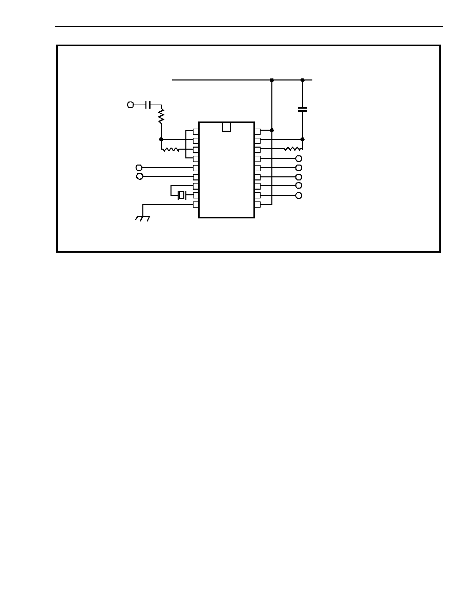
Figure 6 - Single-Ended Input Configuration
IN+
IN-
GS
V
Ref
INH
PDWN
OSC1
OSC2
V
SS
V
DD
St/GT
ESt
StD
Q4
Q3
Q2
Q1
TOE
DTMF
Input
C
1
V
DD
R
1
R
2
X-tal
MT88L70
C
2
R
3
NOTES:
R
1
, R
2
= 100 k
±
1%
R
3
= 300 k
±
1%
C
1
,C
2
= 100 nF
±
5%
X-tal = 3.579545 MHz
±
0.1%
V
DD
= 3.0V + 20% / -10%
the input pins are connected as shown in Figure 6
with the op-amp connected for unity gain and V
Ref
biasing the input at 1/2V
DD
. Figure 5 shows the
differential configuration, which permits the
adjustment of gain with the feedback resistor R
5
.
Crystal Oscillator
The internal clock circuit is completed with the
addition of an external 3.579545 MHz crystal and is
connected as shown in Figure 6 (Single-ended Input
Configuration).
Applications
A single-ended input configuration is shown in Figure
6. For applications with differential signal inputs the
circuit shown in Figure 5 may be used.