 | –≠–ª–µ–∫—Ç—Ä–æ–Ω–Ω—ã–π –∫–æ–º–ø–æ–Ω–µ–Ω—Ç: MT8940-1 | –°–∫–∞—á–∞—Ç—å:  PDF PDF  ZIP ZIP |
27
3-27
Æ
Features
∑
Provides T1 clock at 1.544 MHz locked to input
frame pulse
∑
Sources CEPT (30+2) Digital Trunk/ST-BUS
clock and timing signals locked to internal or
external 8 kHz signal
∑
TTL compatible logic inputs and outputs
∑
Uncommitted 2-input NAND gate
∑
Single 5 volt power supply
∑
Low power ISO-CMOS technology
Applications
∑
Synchronization and timing control for T1
and CEPT digital trunk transmission links
∑
ST- BUS clock and frame pulse source
Description
The MT8940 is a dual digital phase-locked loop
providing the timing and synchronization signals for
the T1 or CEPT transmission links and the ST-BUS.
The first PLL provides the T1 clock (1.544 MHz)
synchronized to the input frame pulse at 8 kHz. The
timing signals for the CEPT transmission link and the
ST-BUS are provided by the second PLL locked to an
internal or an external 8 kHz frame pulse signal.
The MT8940 is fabricated in MITEL's ISO-CMOS
technology.
Ordering Information
MT8940AE
24 Pin Plastic DIP (600 mil)
-40
∞
C to +85
∞
C
Figure 1 - Functional Block Diagram
F0i
C12i
MS0
MS1
MS2
MS3
C8Kb
C16i
Ai
Bi
Yo
V
DD
V
SS
RST
CVb
CV
ENCV
F0b
C4b
C4o
ENC4o
C2o
C2o
ENC2o
2:1 MUX
Variable
Clock
Control
Mode
Selection
Logic
DPLL #2
Input
Selector
Clock
Generator
Frame Pulse
Control
4.096 MHz
Clock
Control
2.048 MHz
Clock
Control
DPLL #1
ISSUE 8
March 1997
MT8940
T1/CEPT Digital Trunk PLL
ISO-CMOS ST-BUS
TM
FAMILY
MT8940
ISO-CMOS
3-28
Figure 2 - Pin Connections
Pin Description
Pin #
Name
Description
1
EN
CV
Variable clock enable (TTL compatible input) - This input (pulled internally to V
DD
) directly
controls the three states of CV (pin 22) under all modes of operation. When HIGH, enables
CV and when LOW, puts it in high impedance condition. It also controls the three states of
CVb signal (pin 21) if MS1 is LOW. When EN
CV
is HIGH, the pin CVb is an output and when
LOW, it is in high impedance state. However, if MS1 is HIGH, CVb is always an input.
2
MS0
Mode select `0' input (TTL compatible) - This input (pulled internally to V
SS
) in conjunction
with MS1 (pin 4) selects the major mode of operation for both DPLLs. (Refer to Tables 1 and
2).
3
C12i
Clock 12.355 MHz input (TTL compatible) - Master clock input at 12.355 MHz
±
100ppm for
DPLL #1.
4
MS1
Mode select-1 input (TTL compatible) - This input (pulled internally to V
SS
) in conjunction
with MS0 (pin 2) selects the major mode of operation for both DPLLs. (Refer to Tables 1 and
2)
5
F0i
Frame pulse input (TTL compatible) - This is the frame pulse input (pulled internally to
V
DD
) at 8 kHz. The DPLL #1 locks to the falling edge of this input to generate T1 (1.544
MHz) clock.
6
F0b
Frame pulse Bidirectional (TTL compatible input and Totem-pole output) - Depending
on the minor mode selected for the DPLL #2, it provides the 8 kHz frame pulse output or acts
as an input (pulled internally to V
DD
) to an external frame pulse.
7
MS2
Mode select-2 input (TTL compatible) - This input (pulled internally to V
DD
) in conjunction
with MS3 (pin 17) selects the minor mode of operation for the DPLL #2. (Refer to Table 3.)
8
C16i
Clock 16.388 MHz input (TTL compatible) - Master clock input at 16.388 MHz
±
32 ppm for
DPLL #2.
9
EN
C4o
Enable 4.096 MHz clock (TTL compatible input) - This active high input (pulled internally
to V
DD
) enables C4o (pin 11) output. When LOW, the output C4o is in high impedance
condition.
1
2
3
4
5
6
7
8
9
10
11
12
13
14
15
16
24
23
22
21
20
19
18
17
ENVC
MS0
C12i
MS1
F0i
F0b
MS2
C16i
ENC4o
C8Kb
C4o
VSS
VDD
RST
CV
CVb
Yo
Bi
Ai
MS3
ENC2o
C2o
C2o
C4b

ISO-CMOS
MT8940
3-29
10
C8Kb
Clock 8 kHz- Bidirectional (TTL compatible input and open drain output with 100K
internal resistor to V
DD
) - This is the 8 kHz input signal on the rising edge of which DPLL #2
locks during its NORMAL mode. When DPLL #2 is in SINGLE CLOCK mode, this pin outputs
an 8 kHz signal provided by DPLL #1, which is also connected internally to DPLL #2.
11
C4o
Clock 4.096 MHz (Three state output) - This is the inverse of the signal appearing on pin
13 (C4b) at 4.096 MHz and has a rising edge in the frame pulse (F0b) window. The high
impedance state of this output is controlled by EN
C4o
(pin 9).
12
V
SS
Ground (0 Volt)
13
C4b
Clock 4.096 MHz- Bidirectional (TTL compatible input and Totem-pole output) - When
the mode select bit MS3 (pin 17) is HIGH, it provides the 4.096 MHz clock output with the
falling edge in the frame pulse (F0b) window. When pin 17 is LOW, C4b is an input (pulled
internally to V
DD
) to an external clock at 4.096 MHz.
14
C2o
Clock 2.048 MHz (Three state output) - This is the divide by two output of C4b (pin 13) and
has a falling edge in the frame pulse (F0b) window. The high impedance state of this output
is controlled by EN
C2o
(pin 16).
15
C2o
Clock 2.048 MHz (Three state output) - This is the divide by two output of C4b (pin 13) and
has a rising edge in the frame pulse (F0b) window. The high impedance state of this output is
controlled by EN
C2o
(pin 16).
16
EN
C2o
Enable 2.048 MHz clock (TTL compatible input) - This active high input (pulled internally
to V
DD
) enables both C2o and C2o outputs (pins 14 and 15). When LOW, these outputs are
in high impedance condition.
17
MS3
Mode select 3 input (TTL compatible) - This input (pulled internally to V
DD
) in conjunction
with MS2 (pin 7) selects the minor mode of operation for DPLL #2. (Refer to Table 3.)
18,19
Ai, Bi
Inputs A and B (TTL compatible) -These are the two inputs (pulled internally to V
SS
) of the
uncommitted NAND gate
.
20
Y
o
Output Y (Totem pole output) - Output of the uncommitted NAND gate.
21
CVb
Variable clock Bidirectional (TTL compatible input and Totem-pole output) - When
acting as an output (MS1-LOW) during the NORMAL mode of DPLL #1, this pin provides the
1.544 MHz clock locked to the input frame pulse F0i (pin 5). When MS1 is HIGH, it is an
input (pulled internally to V
DD
) to an external clock at 1.544 MHz or 2.048 MHz to provide the
internal signal at 8 kHz to DPLL #2.
22
CV
Variable clock (Three state output) - This is the inverse output of the signal appearing on
pin 21, the high impedance state of which is controlled EN
CV
(pin 1).
23
RST
Reset (Schmitt trigger input) -This input (active LOW) evokes reset condition for the
device.
24
V
DD
V
DD
(+5V) Power supply.
Pin Description (continued)
Pin #
Name
Description
MT8940
ISO-CMOS
3-30
Functional Description
The MT8940 is a dual digital phase-locked loop
providing the timing and synchronization signals to
the interface circuits for T1 and CEPT (30+2)
Primary Multiplex Digital Transmission links. As
shown in Figure 1, it has two digital phase-locked
loops (DPLLs), associated output controls and the
mode selection logic circuits. The two DPLLs,
although similar in principle, operate independently
to provide T1 (1.544 MHz) and CEPT (2.048 MHz)
transmission clocks, and ST-BUS timing signals.
The principle of operation behind the two DPLLs is
shown in Figure 3. A master clock is divided down to
8 kHz where it is compared with the 8 kHz input, and
depending on the output of the phase comparison,
the master clock frequency is corrected. The
MT8940 achieves the frequency correction in both
directions by using the master clock at a slightly
higher frequency and dividing it unaltered or
stretching its period (at two discrete instants in a
frame) before the division depending on the phase
comparison output. When the input frequency is
Figure 3 - DPLL Principle
higher, the unchanged master clock is divided, thus
effectively speeding-up the locally generated clock
and eventually pulling it in synchronization with the
input. If the input frequency is lower than the divided
master clock, the period of the master clock is
stretched by half a cycle, at two discrete instants in a
phase sampling period. This introduces a total delay
of one master clock period over the sampling
duration, which is then divided to generate the local
signal synchronous with the input. Once the output is
phase-locked to the active edge of the input, the
circuit will maintain the locked condition as long as
the input frequency is within the lock-in range (
±
1.04
Hz) of the DPLLs. The lock-in range is wide enough
to meet the CCITT line rate specification (1.544
MHz
±
130ppm and 2.048 MHz
±
50ppm) for the High
Capacity Terrestrial Digital Service.
The phase sampling is done once in a frame (8 kHz)
and the divisions are set at 8 and 193 for DPLL #1,
which locks on to the falling edge of the input at 8
kHz to generate T1 (1.544 MHz) clock. Although the
phase sampling duration is the same for DPLL #2,
the divisions are set at 8 and 256 to provide the
CEPT/ST-BUS clock at 2.048 MHz synchronized to
the rising edge of the input signal (8 kHz). The
master clock source is specified to be at 12.355 MHz
±
100 ppm for DPLL #1 and 16.388 MHz
±
32 ppm for
DPLL #2 over the entire temperature range of
operation.
The inputs MS0 to MS3 are used to select the
operating mode of the MT8940, see Tables 1 to 4. All
the outputs are individually controlled to the high
impedance condition by their respective enable
controls. The uncommitted NAND gate is available
for use in applications involving MITEL's
MT8976/MH89760 (T1 interfaces) and
MT8979/MH89790 (CEPT interfaces).
Modes of Operation
The operation of the MT8940 is categorized into
major and minor modes. The major modes are
defined for both DPLLs by the mode select pins MS0
and MS1. The minor modes are selected by MS2
and MS3, and are applicable only to DPLL #2. There
are no minor modes for DPLL #1.
Major modes of the DPLL #1
DPLL #1 can be operated in three major modes as
selected by MS0 and MS1 (Table 1). When MS1 is
LOW, it is in NORMAL mode, which provides a T1
(1.544 MHz) clock signal locked to the falling edge of
the input frame pulse F0i (8 kHz). DPLL#1 requires a
master clock input of 12.355 MHz
±
100 ppm (C12i).
In the second and third major modes (MS1 is HIGH),
DPLL #1 is set to DIVIDE an external 1.544 MHz or
2.048 MHz signal applied at CVb (pin 21). The
division can be set by MS0 to be either 193 (LOW) or
256 (HIGH). In these modes, the 8 kHz output is
connected internally to DPLL #2, which operates in
SINGLE CLOCK mode.
Major modes of the DPLL #2
There are four major modes for DPLL #2 selectable
by MS0 and MS1, as shown in Table 2. In all these
modes DPLL #2 provides the CEPT PCM 30 timing,
and the ST-BUS clock and framing signals.
In NORMAL mode, DPLL #2 provides the CEPT and
ST-BUS compatible timing signals locked to the
rising edge of the 8 kHz input signal (C8Kb). These
Master Clock
(12.355 MHz/
16.388 MHz)
Frequency
Correction
˜
8
Output
(1.544 MHz /
Input (8 kHz)
Phase
Comparison
˜
193 /
˜
256
2.048 MHz)

ISO-CMOS
MT8940
3-31
signals are the 4.096 MHz (C4o and C4b) and the
2.048 MHz (C2o and C2o) clocks, and the 8 kHz
Note: X: indicates don't care
Table 1. Major Modes of the DPLL #1
frame pulse (F0b), which are derived from the 16.388
MHz master clock. This mode can also provide the
ST-BUS timing and framing signals with the input
(C8Kb) tied HIGH and the master clock set at 16.384
MHz. The DPLL makes no correction in this
configuration and provides the timing signals
compatible to the ST-BUS format without any jitter.
In FREE-RUN mode, DPLL #2 generates CEPT and
ST-BUS timing and framing signals with no external
inputs except the master clock set at 16.388 MHz.
Since the master clock source is set at a higher
frequency than the nominal value, the DPLL makes
the necessary corrections to deliver the averaged
timing signals compatible to the ST-BUS format.
The operation of DPLL #2 in SINGLE CLOCK-1
mode is identical to SINGLE CLOCK-2 mode,
providing the CEPT and ST-BUS compatible timing
signals synchronized to the internal 8 kHz signal
obtained from DPLL#1 in DIVIDE mode. When
SINGLE CLOCK-1 mode is selected for DPLL #2, it
automatically selects the DIVIDE-1 mode for DPLL
#1, and thus, an external 1.544 MHz clock signal
applied at CVb (pin 21) is divided by DPLL #1 to
generate the internal signal at 8 kHz onto which
DPLL #2 locks. Similarly when SINGLE CLOCK-2
mode is selected, DPLL #1 is in DIVIDE-2 mode,
with an external signal of 2.048 MHz providing the
internal 8 kHz signal to DPLL #2. In both these
modes, this internal signal is available on C8Kb (pin
10) and DPLL #2 locks to its falling edge to provide
the CEPT and ST-BUS compatible timing signals.
This is in contrast to the Normal mode where these
timing signals are synchronized with the rising edge
of the 8 kHz signal on C8Kb.
Minor modes of the DPLL #2
The minor modes for DPLL #2 depends upon the
status of the mode select bits MS2 and MS3 (pins 7
and 17).
Table 2. Major Modes of the DPLL #2
When MS3 is HIGH, DPLL #2 operates in any of the
major modes as selected by MS0 and MS1.
When MS3 is LOW, it overrides the major mode
selected and DPLL #2 accepts an external clock of
4.096 MHz on C4b (pin 13) to provide the 2.048 MHz
clocks (C2o and C2o) and the 8 kHz frame pulse
(F0b) compatible with the ST-BUS format.
The mode select bit MS2, controls the signal
direction of F0b (pin 6). When MS2 is LOW, F0b is an
input for an external frame pulse at 8 kHz. This
Table 3. Minor Modes of the DPLL #2
input is effective only if MS3 is also LOW and C4b is
accepting a 4.096 MHz external clock, which has a
proper phase relationship with the external input on
MS0
MS1
Mode of
operation
Function
X
0
NORMAL
Provides the T1 (1.544
MHz) clock synchronized
to the falling edge of the
input frame pulse (F0i).
0
1
DIVIDE-1
DPLL #1 divides the CVb
input by 193. The divided
output is connected to
DPLL #2.
1
1
DIVIDE-2
DPLL #1 divides the CVb
input by 256. The divided
output is connected to
DPLL #2.
MS0
MS1
Mode of
operation
Function
0
0
NORMAL
Provides ST-BUS/CEPT
timing signals locked to the
rising edge of the 8kHz
input signal at C8Kb.
1
0
FREE-RUN Provides ST-BUS timing
and framing signals with no
external inputs, except the
master clock.
0
1
SINGLE
CLOCK-1
Provides the CEPT/ST-
BUS compatible timing
signals locked to the falling
edge of the 8kHz internal
signal provided by DPLL
#1.
1
1
SINGLE
CLOCK-2
Provides CEPT/ST-BUS
timing signals locked to the
falling edge of the 8kHz
internal signal provided by
DPLL #1.
MS2
MS3
Functional Description
1
1
Provides ST-BUS 4.096 MHz and 2.048
MHz clocks and 8kHz frame pulse
depending on the major mode selected.
0
1
Provides ST-BUS 4.096 MHz & 2.048 MHz
clocks depending on the major mode
selected while F0b acts as an input.
However, the input on F0b has no effect on
the operation of DPLL #2 unless it is in
FREE-RUN mode.
0
0
Overrides the major mode selected and
accepts properly phase related external
4.096 MHz clock and 8 kHz frame pulse to
provide the ST-BUS compatible clock at
2.048MHz.
1
0
Overrides the major mode selected and
accepts a 4.096 MHz external clock to
provide the ST-BUS clock and frame pulse
at 2.048 MHz and 8 kHz, respectively.

MT8940
ISO-CMOS
3-32
F0b (refer to Figure 15). Otherwise, the input on pin
F0b will have no bearing on the operation of DPLL
#2, unless it is in FREE-RUN mode as selected by
MS0 and MS1. In FREE-RUN mode, the input on
F0b is treated the same way as the C8Kb input in
NORMAL mode. The frequency of the input signal on
F0b should be 16 kHz for DPLL #2 to provide the ST-
BUS compatible clocks at 4.096 MHz and 2.048
MHz.
When MS2 is HIGH, the F0b pin provides the ST-
BUS frame pulse output locked to the 8kHz internal
or external signal as determined by the other mode
select pins MS0, MS1 and MS3.
Table 4 summarizes the modes of the two DPLLs. It
should be noted that each of the major modes
selected for DPLL #2 can have any of the minor
modes, although some of the combinations are
functionally similar. The required operation of both
DPLL#1 and DPLL#2 must be considered when
determining MS0-MS3.
Table 4. Summary of Modes of Operation - DPLL #1 and #2
M
O
D
E
#
MS
0
MS
1
MS
2
MS
3
Operating Modes
DPLL #1
DPLL #2
0
0
0
0
0
NORMAL MODE
Properly phase related External 4.096 MHz
clock and 8 kHz frame pulse provide the ST-
BUS clock at 2.048 MHz.
1
0
0
0
1
NORMAL MODE
NORMAL MODE
F0b is an input but has no function in this mode.
2
0
0
1
0
NORMAL MODE
External 4.096 MHz provides the ST-BUS clock
and Frame Pulse at 2.048 MHz and 8 kHz,
respectively.
3
0
0
1
1
NORMAL MODE:
Provides the T1 (1.544 MHz) clock
synchronized to the falling edge of the
input frame pulse (F0i).
NORMAL MODE:
Provides the CEPT/ST-BUS compatible timing
signals locked to the 8 kHz input signal (C8Kb).
4
0
1
0
0
DIVIDE-1 MODE
Same as mode `0'.
5
0
1
0
1
DIVIDE-1 MODE
SINGLE CLOCK-1 MODE
F0b is an input, but has no function in this
mode.
6
0
1
1
0
DIVIDE-1 MODE
Same as mode 2.
7
0
1
1
1
DIVIDE-1 MODE:
Divides the CVb input by 193. The divided
output is connected to DPLL #2.
SINGLE CLOCK-1 MODE:
Provides the CEPT/ST-BUS compatible timing
signals locked to the 8 kHz internal signal
provided by DPLL #1.
8
1
0
0
0
NORMAL MODE
Same as mode `0'.
9
1
0
0
1
NORMAL MODE
F0b is an input and DPLL #2 locks on to
it only if it is at 16 kHz to provide the ST-BUS
control signals.
10
1
0
1
0
NORMAL MODE
Same as mode 2.
11
1
0
1
1
NORMAL MODE
Provides the T1 (1.544 MHz) clock
synchronized to the falling edge of input frame
pulse (F0i).
FREE-RUN MODE:
Provides the ST-BUS timing signals with no
external inputs except the master clock.
12
1
1
0
0
DIVIDE-2 MODE
Same as mode `0'.
13
1
1
0
1
DIVIDE-2 MODE
SINGLE CLOCK-2 MODE:
F0b is an input, but has no function in this
mode.
14
1
1
1
0
DIVIDE-2 MODE
Same as mode 2.
15
1
1
1
1
DIVIDE-2 MODE:
Divides the CVb input by 256. The divided
output is connected to DPLL#2.
SINGLE CLOCK-2 MODE:
Provides the CEPT/ST-BUS compatible timing
signals locked to the 8 kHz internal signal
provided by DPLL #1.
ISO-CMOS
MT8940
3-33
Applications
The following figures illustrate how the MT8940 can
be used in a minimum component count approach to
providing the timing and synchronization signals for
the Mitel T1 and CEPT interfaces, and the ST-BUS.
The hardware selectable modes and the
independent control over each PLL adds flexibility to
the interface circuits. It can be easily reconfigured to
provide the timing and control signals for both at the
master and slave ends of the link.
Synchronization and Timing Signals for the T1
Transmission Link
Figures 4 and 5 show examples of how to generate
the timing signals for the master and slave ends of a
T1 link.
At the master end of the link (Figure 4), DPLL #2 is
the source of the ST-BUS signals derived from the
4.096 MHz system clock. The frame pulse output is
looped back to DPLL #1 (in NORMAL mode), which
locks to it to generate the T1 line clock. The timing
relationship between the 1.544 MHz T1 clock and the
2.048 MHz ST-BUS clock meets the requirements of
the MH89760/760B. The crystal clock at 12.355 MHz
is used by DPLL #1 to generate the 1.544 MHz clock,
while DPLL #2 uses the 4.096 MHz system clock to
provide the ST-BUS timing signals. The ST-BUS
signals can also be obtained from DPLL #2 in FREE-
RUN mode, using a crystal clock at 16.388 MHz
instead of 4.096 MHz system clock. The
uncommitted NAND gate converts the received
signals, RxA and RxB of the MH89760 to a single
Return to Zero (RZ) input for the clock extraction
circuits of the MH89760. This is not required for the
MH89760B. The generated ST-BUS signals can be
used to synchronize the system and the switching
equipment at the master end.
At the slave end of the link (Figure 5) both the DPLLs
are in NORMAL mode with DPLL #2 providing the
ST-BUS timing signals locked to the 8 kHz frame
pulse (E8Ko) extracted from the received signal on
the T1 line. The regenerated frame pulse is looped
back to DPLL #1 to provide the T1 line clock as at
the master end. The 12.355 MHz and 16.388 MHz
crystal clock sources are necessary for DPLL #1 and
#2.
Synchronization and Timing Signals for the
CEPT Transmission Link
The MT8940 can be used to provide the timing and
synchronization signals for the MH89790/790B,
MITEL's CEPT(30+2) digital trunk interface hybrid.
Since the operational frequencies of the ST-BUS and
the CEPT primary multiplex digital trunk are same,
only DPLL #2 is required to achieve synchronization
between the two
.
Figures 6 and 7 show how the MT8940 can be used
to synchronize the ST-BUS and the CEPT
transmission link at the master and slave ends,
respectively.
Figure 4 - Synchronization at the Master End of the T1 Transmission Link
Crystal Clock
(12.355 MHz
±
100 ppm)
4.096 MHz
System Clock
(ST-BUS
compatible)
MT8940
MS0
MS1
MS2
MS3
F0i
C12i
EN
CV
C8Kb
C16i
EN
C4o
EN
C2o
Ai
Bi
V
SS
V
DD
CV
C4b
C2o
F0b
Y
o
RST
MH89760
C1.5i
C2i
F0i
RxA
RxB
RxD
DSTi
DSTo
CSTi
CSTo
TxT
TxR
RxT
RxR
MT8980/81
ST-BUS
SWITCH
T1
LINK
(1.544 Mbps)
TRANSMIT
RECEIVE
MODE OF OPERATION FOR THE MT8940
DPLL #1 - NORMAL (MS0 = X; MS1 = 0)
DPLL #2 - OVERRIDE THE MAJOR MODES (MS2 = 1; MS3 = 0)
MT8940
ISO-CMOS
3-34
Figure 5 - Synchronization at the Slave End of the T1 Transmission Link
Figure 6 - Synchronization at the Master End of the CEPT Digital Transmission Link
Crystal Clock
(12.355 MHz
±
100 ppm)
MT8940
MS0
MS1
MS2
MS3
F0i
C12i
EN
CV
C8Kb
C16i
EN
C4o
EN
C2o
Ai
Bi
V
SS
V
DD
CV
C4b
C2o
F0b
Y
o
RST
MH89760
C1.5i
C2i
F0i
RxA
RxB
RxD
DSTi
DSTo
CSTi
CSTo
TxT
TxR
RxT
RxR
MT8980/81
ST-BUS
SWITCH
T1
LINK
(1.544 Mbps)
Mode of Operation for the MT8940
DPLL #1 - NORMAL (MS1=0)
DPLL #2 - NORMAL (MS0=0; MS1=0; MS2=1; MS3=1)
Crystal Clock
(16.388 MHz
±
32 ppm)
TRANSMIT
RECEIVE
MT8940
MS0
MS1
MS2
MS3
F0i
C12i
EN
CV
C8Kb
C16i
EN
C4o
EN
C2o
Ai
Bi
V
SS
V
DD
C4b
C2o
F0b
Y
o
RST
MH89790
C2i
F0i
RxA
RxB
RxD
DSTi
DSTo
CSTi0
CSTi1
CSTo
OUTA
OUTB
RxT
TRANSMIT
RECEIVE
MT8980/81
ST-BUS
SWITCH
RxR
CEPT
PRIMARY
MULTIPLEX
DIGITAL
LINK
4.096 MHz
System Clock
(ST-BUS
Compatible)
Mode of Operation for the MT8940
DPLL #1 - NOT USED
DPLL #2 - OVERRIDE MAJOR MODES (MS0=X; MS1=X
MS2=1; MS3=0)
Generation of ST-BUS Timing Signals
The MT8940 can source the properly formatted ST-
BUS timing and control signals with no external
inputs except the crystal clock. This can be used as
the standard timing source for ST-BUS systems or
any other system with similar clock requirements.
Figure 8 shows two such applications using only
DPLL #2. In one case, the MT8940 is in FREE-RUN
mode with an oscillator input of 16.388 MHz. This
forces the DPLL to correct at a rate of 4 kHz to
maintain the ST-BUS clocks, which therefore, will be
jittered. In the other case, the oscillator input is
16.384 MHz (exactly eight times the output
frequency) and DPLL #2 operates in NORMAL mode
with C8Kb input tied HIGH. Since no corrections are
necessary, the output is free from jitter. DPLL #1 is
completely free in both cases and available for any
other purpose.

ISO-CMOS
MT8940
3-35
Figure 7 - Synchronization at the Slave End of the CEPT Digital Transmission Link
Figure 8 - Generation of the ST-BUS Timing Signals
TRANSMIT
RECEIVE
MT8980/81
ST-BUS
SWITCH
MH89790
C2i
F0i
RxA
RxB
RxD
DSTi
DSTo
CSTi0
CSTi1
CSTo
OUTA
OUTB
RxT
RxR
MT8940
MS0
MS1
MS2
MS3
F0i
C12i
EN
CV
C8Kb
C16i
EN
C4o
EN
C2o
Ai
Bi
V
SS
V
DD
C4b
C2o
F0b
Y
o
RST
CEPT
PRIMARY
MULTIPLEX
DIGITAL
LINK
Crystal Clock
(16.388 MHz
±
32 ppm)
Mode of Operation for the MT8940
DPLL #1 - NOT USED
DPLL #2 - NORMAL (MS0=0; MS1=0; MS2=1; MS3=1)
MT8940
MS0
MS1
MS2
MS3
F0i
C12i
EN
CV
C8Kb
C16i
EN
C4o
EN
C2o
Ai
Bi
V
SS
V
DD
C4b
RST
Crystal Clock
(16.388 MHz
±
32 ppm)
Crystal Clock
(16.388 MHz
±
32 ppm)
C4o
C2o
C2o
F0b
MT8940
MS0
MS1
MS2
MS3
F0i
C12i
EN
CV
C8Kb
C16i
EN
C4o
EN
C2o
Ai
Bi
V
SS
V
DD
C4b
RST
C4o
C2o
C2o
F0b
DPLL #1 - NOT USED
DPLL #2 - NORMAL MODE
(MS0=0; MS1=0;
MS2=1; MS3=1)
DPLL #1 - NOT USED
DPLL #2 - NORMAL MODE
(MS0=0; MS1=0; MS2=1;
MS3=1)
ST-BUS
TIMING
SIGNALS
ST-BUS
TIMING
SIGNALS
MT8940
ISO-CMOS
3-36
* Exceeding these values may cause permanent damage. Functional operation under these conditions is not implied.
Typical figures are at 25
∞
C and are for design aid only: not guaranteed and not subject to production testing.
Typical figures are at 25
∞
C and are for design aid only: not guaranteed and not subject to production testing.
Absolute Maximum Ratings*
- Voltages are with respect to ground (V
SS
) unless otherwise stated.
Parameter
Symbol
Min
Max
Units
1
Supply Voltage
V
DD
-0.3
7.0
V
2
Voltage on any pin
V
I
V
SS
-0.5
V
DD
+0.5
V
3
Input/Output Diode Current
I
IK/OK
±
10
mA
4
Output Source or Sink Current
I
O
±
25
mA
5
DC Supply or Ground Current
I
DD
/I
SS
±
50
mA
6
Storage Temperature
T
ST
-65
150
o
C
7
Package Power Dissipation
LCC
P
D
600
mW
Recommended Operating Conditions
- Voltages are with respect to ground (V
SS
) unless otherwise stated.
Characteristics
Sym
Min
Typ
Max
Units
Test Conditions
1
Supply Voltage
V
DD
4.75
5.0
5.25
V
2
Input HIGH Voltage
V
IH
2.4
V
DD
V
For 400 mV noise margin
3
Input LOW Voltage
V
IL
V
SS
0.4
V
For 400 mV noise margin
4
Operating Temperature
T
A
-40
25
85
o
C
DC Electrical Characteristics
- Voltages are with respect to ground (V
SS
) unless otherwise stated.
V
DD
=5.0 V
±
5%; V
SS
=0V; T
A
=-40 to 85
∞
C.
Characteristics
Sym
Min
Typ
Max
Units
Test Conditions
1
S
U
P
Supply Current
I
DD
I
DDS
8
15
100
mA
Under clocked condition, with the
inputs tied to the same supply rail
as the corresponding pull-up /
down resistors.
2
I
N
Input HIGH voltage (For all the
inputs except pin 23)
V
IH
2.0
V
3
Positive-going threshold
voltage (For pin 23)
V
+
2.8
V
4
Input LOW voltage (For all the
inputs except pin 23)
V
IL
0.8
V
5
Negative-going threshold
voltage (For pin 23)
V
-
1.5
V
6
O
U
T
Output current HIGH (For all
the outputs except pin 10)
I
OH
-9.5
mA
V
OH
=2.4 V
7
Output current LOW (For all the
outputs except pin 10)
I
OL
4.5
mA
V
OL
=0.4 V
8
Output current LOW (pin 10)
I
OL
2.0
mA
V
OL
=0.4 V
9
Leakage current on bidirect-
ional pins and all inputs except
C12i, C16i, RST
I
IZ/OZ
±
150
µ
A
V
I/O=
V
SS
or V
DD
10
Leakage current on all outputs
and C12i, C16i, RST inputs
I
IZ/OZ
±
1
±
10
µ
A
V
I/O
=V
SS
or V
DD

ISO-CMOS
MT8940
3-37
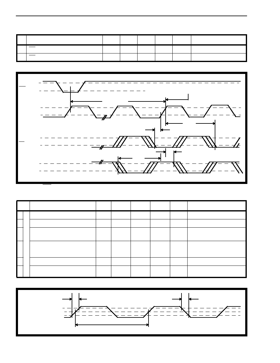
Timing is over recommended temperature & power supply voltages.
Typical figures are at 25
∞
C and are for design aid only: not guaranteed and not subject to production testing.
Figure 9 - Timing Information for DPLL #1 in NORMAL Mode
Timing is over recommended temperature & power supply voltages.
Typical figures are at 25
∞
C and are for design aid only: not guaranteed and not subject to production testing.
AC Electrical Characteristics
-
Voltages are with respect to ground (V
SS
) unless otherwise stated.
(Ref. Figure 9)
Characteristics
Sym
Min
Typ
Max
Units
Test Conditions
1
D
P
L
L
#1
Frame pulse input (F0i) to CVb
output (1.544 MHz) delay
t
F15H
-40
75
ns
2
CVb output (1.544 MHz) rise
time
t
r1.5
10
15
ns
Test load circuit 1 (Fig. 17).
3
CVb output (1.544 MHz) fall
time
t
f1.5
12
15
ns
Test load circuit 1 (Fig. 17).
4
CVb output (1.544 MHz) clock
period
t
P15
648
690
ns
5
CVb output (1.544 MHz) clock
width (HIGH)
t
W15H
320
386
ns
6
CVb output (1.544 MHz) clock
width (LOW)
t
W15L
314
327
ns
7
CV delay (HIGH to LOW)
t
15HL
5
30
ns
8
CV delay (LOW to HIGH)
t
15LH
-12
10
ns
AC Electrical Characteristics
-
Voltages are with respect to ground (V
SS
) unless otherwise stated.
(Ref. Figure 10)
Characteristics
Sym
Min
Typ
Max
Units
Test Conditions
1
D
P
L
L
#1
C8Kb output (8kHz) delay
(HIGH to HIGH)
t
C8HH
130
ns
Test load circuit 2 (Fig. 17).
2
C8Kb output (8 kHz) delay
(LOW to LOW)
t
C8LL
50
130
ns
Test load circuit 2 (Fig. 17).
3
C8Kb output duty cycle
66
50
%
%
In Divide -1 Mode
In Divide - 2 Mode
4
Inverted clock output delay
(HIGH to LOW)
t
ICHL
40
75
ns
5
Inverted clock output delay
(LOW to HIGH)
t
ICLH
35
60
ns
F0i
CVb
CV
V
IH
V
IL
V
OH
V
OL
V
OH
V
OL
t
F15H
t
f1.5
t
15HL
t
15LH
t
r1.5
t
P15
t
W15H
t
W15L
MT8940
ISO-CMOS
3-38
Figure 10 - DPLL #1 in DIVIDE Mode
Figure 11 - Timing Information on DPLL #2 Outputs
CVb
CV
C8Kb
V
IH
V
IL
V
OH
V
OL
V
OH
V
OL
t
ICHL
t
ICLH
t
C8HH
t
C8LL
V
OH
V
OL
V
OH
V
OL
V
OH
V
OL
V
OH
V
OL
V
OH
V
OL
F0b
C4b
C4o
C2o
C2o
t
FPL
t
FPH
t
fC4
t
rC4
t
4oLH
t
4oHL
t
42LH
t
42HL
t
fC2
t
rC2
t
2oLH
t
2oHL
t
WFP
t
P2o
t
W2oH
t
W2oL
ISO-CMOS
MT8940
3-39
Timing is over recommended temperature & power supply voltages.
Typical figures are at 25
∞
C and are for design aid only: not guaranteed and not subject to production testing.
Figure 12 - ST-BUS Timings from DPLL #2 and C8Kb Input/Output
AC Electrical Characteristics
-Voltages are with respect to ground (V
SS
) unless otherwise stated.
(Ref. Figures 11&12)
Characteristics
Sym
Min
Typ
Max
Units
Test Conditions
1
D
P
L
L
#2
C4b output delay (HIGH to
LOW) from C8Kb input/output
t
84H
-25
75
ns
Test load circuit 2 (Fig. 17)
on C8Kb.
2
C4b output clock period
t
P4o
240
282
ns
Test load circuit 1 (Fig. 17).
3
C4b output clock width (HIGH)
t
W4oH
123
165
ns
4
C4b output clock width (LOW)
t
W4oL
110
123
ns
5
C4b output clock rise time
t
rC4
10
ns
Test load circuit 1 (Fig. 17).
6
C4b clock output fall time
t
fC4
10
ns
Test load circuit 1 (Fig. 17).
7
Frame pulse output delay
(HIGH to LOW) from C4b
t
FPL
50
ns
Test load circuit 1 (Fig. 17).
8
Frame pulse output delay
(LOW to HIGH) from C4b
t
FPH
40
ns
Test load circuit 1 (Fig. 17).
9
Frame pulse (F0b) width
t
WFP
200
245
ns
10
C4o delay - LOW to HIGH
t
4oLH
45
ns
11
C4o delay - HIGH to LOW
t
4oHL
45
ns
12
C4b to C2o delay (LOW to
HIGH)
t
42LH
-10
+10
ns
13
C4b to C2o delay (HIGH to
LOW)
t
42HL
20
ns
14
C2o clock period
t
P2o
486
523
ns
Test load circuit 1 (Fig. 10).
15
C2o clock width (HIGH)
t
W2oH
244
291
ns
16
C2o clock width (LOW)
t
W2oL
233
244
ns
17
C2o clock rise time
t
rC2
10
ns
Test load circuit 1 (Fig. 10).
18
C2o clock fall time
t
fC2
10
ns
Test load circuit 1 (Fig. 10).
19
C2o delay - LOW to HIGH
t
2oLH
20
ns
20
C2o delay - HIGH to LOW
t
2oHL
-5
30
ns
V
OH
V
OL
V
OH
V
OL
V
OH
V
OL
V
IH
V
IL
C4b
F0b
C8Kb
as
Output
C8Kb
as
Input
t
84H
t
W4oH
t
P4o
t
FPL
t
FPH
t
W4oL
MT8940
ISO-CMOS
3-40
Timing is over recommended temperature & power supply voltages.
Typical figures are at 25
∞
C and are for design aid only: not guaranteed and not subject to production testing.
Figure 13 - F0b from DPLL #2 is Looped Back as Input to DPLL #1 (T1 Line synchronized to ST-BUS)
Timing is over recommended temperature & power supply voltages
Typical figures are at 25
∞
C and are for design aid only: not guaranteed and not subject to production testing.
Figure 14 - Master Clock Inputs
AC Electrical Characteristics
- Voltages are with respect to ground (V
SS
) unless otherwise stated.
(Ref. Figure 13)
Characteristics
Sym
Min
Typ
Max
Units
Test Conditions
1
CV/CVb (1.544 MHz) Setup time
t
S15
25
ns
2
CV/CVb (1.544 MHz) Hold time
t
H15
110
ns
AC Electrical Characteristics
- Voltages are with respect to ground (V
SS
) unless otherwise stated.
(Ref. Figure 14)
Characteristics
Sym
Min
Typ
Max
Units
Test Conditions
1
C
L
O
C
K
S
Master clocks input rise time
t
r
10
ns
2
Master clocks input fall time
t
f
10
ns
3
Master clock period
(12.355MHz)
t
P12
80.930
80.938
80.946
ns
For DPLL #1, while operating to
provide the T1 clock signal.
4
Master clock period
(16.388MHz)
t
P16
61.018
61.020
61.022
ns
For DPLL #2, while operating to
provide the CEPT and ST-BUS
timing signals.
5
Duty Cycle of master clocks
45
50
55
%
6
Lock-in Range (For each PLL)
-1.5
+1.04
Hz
With the Master clocks as shown
above.
F0b
C2o
CV
CVb
V
OH
V
OL
V
OH
V
OL
V
OH
V
OL
V
OH
V
OL
t
S15
t
H15
Boundary between ST-BUS channel 2 bit 4 and
channel 2 bit 3
20 CYCLES
t
H15
t
S15
Master clock
inputs
2.4 V
1.5 V
0.4 V
t
r
t
f
t
P12
or t
P16

ISO-CMOS
MT8940
3-41
Timing is over recommended temperature & power supply voltages
Typical figures are at 25
∞
C and are for design aid only: not guaranteed and not subject to production testing.
Figure 15 - External Inputs on C4b and F0b for the DPLL #2
Timing is over recommended temperature & power supply voltages
Typical figures are at 25
∞
C and are for design aid only: not guaranteed and not subject to production testing.
Figure 16 - Three State Outputs and Enable Timings
AC Electrical Characteristics
- Voltages are with respect to ground (V
SS
) unless otherwise stated.
(Ref. Figure 15)
Characteristics
Sym
Min
Typ
Max
Units
Test Conditions
1
F0b input pulse width (LOW)
t
WFP
40
ns
2
C4b input clock period
t
P4o
.080
50
µ
s
3
Frame pulse (F0b) setup time
t
FS
25
ns
4
Frame pulse (F0b) hold time
t
FH
5
ns
AC Electrical Characteristics
- Voltages are with respect to ground (V
SS
) unless otherwise stated.
(Ref. Figure 16)
Characteristics
Sym
Min
Typ
Max
Units
Test Conditions
1
O
U
T
P
U
T
Delay from Enable to Output
(HIGH to THREE STATE)
t
PHZ
15
65
ns
Test load circuit 3 (Fig.17)
2
Delay from Enable to Output
(LOW to THREE STATE)
t
PLZ
10
55
ns
Test load circuit 3 (Fig.17)
3
Delay from Enable to Output
(THREE STATE to HIGH)
t
PZH
40
ns
Test load circuit 3 (Fig.17)
4
Delay from Enable to Output
(THREE STATE to LOW)
t
PZL
50
ns
Test load circuit 3 (Fig.17)
F0b
C4b
V
IH
V
IL
V
IH
V
IL
t
FS
t
WFP
t
FH
t
P4o
Enable
Input
Output
LOW to
OFF
Output
HIGH
to OFF
t
f
6 ns
t
r
6 ns
10%
90%
1.3 V
1.3 V
Outputs
Enabled
Outputs
Enabled
Outputs
Disabled
3.0 V
2.7 V
1.3 V
0.3 V
t
PLZ
t
PHZ
t
PZL
t
PZH

MT8940
ISO-CMOS
3-42
Timing is over recommended temperature & power supply voltages.
Typical figures are at 25
∞
C and are for design aid only: not guaranteed and not subject to production testing.
Figure 17 - Test Load Circuits
AC Electrical Characteristics
- Uncommitted NAND Gate
Voltages are with respect to ground (V
SS
) unless otherwise stated.
Characteristics
Sym
Min
Typ
Max
Units
Test Conditions
1
Propagation delay (LOW to
HIGH), input Ai or Bi to output
t
PLH
25
40
ns
Test load circuit 1 (Fig. 17)
2
Propagation delay (HIGH to
LOW), input Ai or Bi to output
t
PHL
20
40
ns
Test load circuit 1 (Fig. 17)
From
output
under test
Test
point
C
L
=50pF
Test load circuit- 1
V
DD
R
L
=1k
Test
point
From
output
under test
Test load circuit- 2
Test load circuit- 3
From
output
under test
C
L
=50pF
C
L
=50pF
Test
point
S
1
V
DD
V
SS
R
L
=1k
Note: S
1
is in position A
when measuring t
PLZ
and t
PZ
and in position B
when measuring t
PHZ
and
t
PZH
A
B
Package Outlines
Plastic Dual-In-Line Packages (PDIP) - E Suffix
NOTE: Controlling dimensions in parenthesis ( ) are in millimeters.
DIM
8-Pin
16-Pin
18-Pin
20-Pin
Plastic
Plastic
Plastic
Plastic
Min
Max
Min
Max
Min
Max
Min
Max
A
0.210 (5.33)
0.210 (5.33)
0.210 (5.33)
0.210 (5.33)
A
2
0.115 (2.92)
0.195 (4.95)
0.115 (2.92)
0.195 (4.95)
0.115 (2.92)
0.195 (4.95)
0.115 (2.92)
0.195 (4.95)
b
0.014 (0.356)
0.022 (0.558)
0.014 (0.356)
0.022 (0.558)
0.014 (0.356)
0.022 (0.558)
0.014 (0.356)
0.022 (0.558)
b
2
0.045 (1.14)
0.070 (1.77)
0.045 (1.14)
0.070 (1.77)
0.045 (1.14)
0.070 (1.77)
0.045 (1.14)
0.070 (1.77)
C
0.008
(0.203)
0.014 (0.356)
0.008 (0.203)
0.014(0.356)
0.008 (0.203)
0.014 (0.356)
0.008 (0.203)
0.014 (0.356)
D
0.355 (9.02)
0.400 (10.16)
0.780 (19.81)
0.800 (20.32)
0.880 (22.35)
0.920 (23.37)
0.980 (24.89)
1.060 (26.9)
D
1
0.005 (0.13)
0.005 (0.13)
0.005 (0.13)
0.005 (0.13)
E
0.300 (7.62)
0.325 (8.26)
0.300 (7.62)
0.325 (8.26)
0.300 (7.62)
0.325 (8.26)
0.300 (7.62)
0.325 (8.26)
E
1
0.240 (6.10)
0.280 (7.11)
0.240 (6.10)
0.280 (7.11)
0.240 (6.10)
0.280 (7.11)
0.240 (6.10)
0.280 (7.11)
e
0.100 BSC (2.54)
0.100 BSC (2.54)
0.100 BSC (2.54)
0.100 BSC (2.54)
e
A
0.300 BSC (7.62)
0.300 BSC (7.62)
0.300 BSC (7.62)
0.300 BSC (7.62)
L
0.115 (2.92)
0.150 (3.81)
0.115 (2.92)
0.150 (3.81)
0.115 (2.92)
0.150 (3.81)
0.115 (2.92)
0.150 (3.81)
e
B
0.430 (10.92)
0.430 (10.92)
0.430 (10.92)
0.430 (10.92)
e
C
0
0.060 (1.52)
0
0.060 (1.52)
0
0.060 (1.52)
0
0.060 (1.52)
E
1
3
2
1
E
n-2 n-1 n
L
D
D
1
b
2
A
2
e
b
C
e
A
Notes:
1) Not to scale
2) Dimensions in inches
3) (Dimensions in millimeters)
A
e
B
e
C
General-8

Package Outlines
Plastic Dual-In-Line Packages (PDIP) - E Suffix
DIM
22-Pin
24-Pin
28-Pin
40-Pin
Plastic
Plastic
Plastic
Plastic
Min
Max
Min
Max
Min
Max
Min
Max
A
0.210 (5.33)
0.250 (6.35)
0.250 (6.35)
0.250 (6.35)
A
2
0.125 (3.18)
0.195 (4.95)
0.125 (3.18)
0.195 (4.95)
0.125 (3.18)
0.195 (4.95)
0.125 (3.18)
0.195 (4.95)
b
0.014 (0.356)
0.022 (0.558)
0.014 (0.356)
0.022 (0.558)
0.014 (0.356)
0.022 (0.558)
0.014 (0.356)
0.022 (0.558)
b
2
0.045 (1.15)
0.070 (1.77)
0.030 (0.77)
0.070 (1.77)
0.030 (0.77)
0.070 (1.77)
0.030 (0.77)
0.070 (1.77)
C
0.008 (0.204)
0.015 (0.381)
0.008 (0.204)
0.015 (0.381)
0.008 (0.204)
0.015 (0.381)
0.008 (0.204)
0.015 (0.381)
D
1.050 (26.67)
1.120 (28.44)
1.150 (29.3)
1.290 (32.7)
1.380 (35.1)
1.565 (39.7)
1.980 (50.3)
2.095 (53.2)
D
1
0.005 (0.13)
0.005 (0.13)
0.005 (0.13)
0.005 (0.13)
E
0.390 (9.91)
0.430 (10.92)
0.600 (15.24)
0.670 (17.02)
0.600 (15.24)
0.670 (17.02)
0.600 (15.24)
0.670 (17.02)
E
0.290 (7.37)
.330 (8.38)
E
1
0.330 (8.39)
0.380 (9.65)
0.485 (12.32)
0.580 (14.73)
0.485 (12.32)
0.580 (14.73)
0.485 (12.32)
0.580 (14.73)
E
1
0.246 (6.25)
0.254 (6.45)
e
0.100 BSC (2.54)
0.100 BSC (2.54)
0.100 BSC (2.54)
0.100 BSC (2.54)
e
A
0.400 BSC (10.16)
0.600 BSC (15.24)
0.600 BSC (15.24)
0.600 BSC (15.24)
e
A
0.300 BSC (7.62)
e
B
0.430 (10.92)
L
0.115 (2.93)
0.160 (4.06)
0.115 (2.93)
0.200 (5.08)
0.115 (2.93)
0.200 (5.08)
0.115 (2.93)
0.200 (5.08)
15
∞
15
∞
15
∞
15
∞
E
1
3
2
1
E
n-2 n-1 n
L
D
D
1
b
2
A
2
e
b
C
e
A
Notes:
1) Not to scale
2) Dimensions in inches
3) (Dimensions in millimeters)
A
e
B
Shaded areas for 300 Mil Body Width 24 PDIP only

M Mitel (design) and ST-BUS are registered trademarks of MITEL Corporation
Mitel Semiconductor is an ISO 9001 Registered Company
Copyright 1999 MITEL Corporation
All Rights Reserved
Printed in CANADA
TECHNICAL DOCUMENTATION - NOT FOR RESALE
World Headquarters - Canada
Tel: +1 (613) 592 2122
Fax: +1 (613) 592 6909
North America
Asia/Pacific
Europe, Middle East,
Tel: +1 (770) 486 0194
Tel: +65 333 6193
and Africa (EMEA)
Fax: +1 (770) 631 8213
Fax: +65 333 6192
Tel: +44 (0) 1793 518528
Fax: +44 (0) 1793 518581
http://www.mitelsemi.com
Information relating to products and services furnished herein by Mitel Corporation or its subsidiaries (collectively "Mitel") is believed to be reliable. However, Mitel assumes no
liability for errors that may appear in this publication, or for liability otherwise arising from the application or use of any such information, product or service or for any infringement of
patents or other intellectual property rights owned by third parties which may result from such application or use. Neither the supply of such information or purchase of product or
service conveys any license, either express or implied, under patents or other intellectual property rights owned by Mitel or licensed from third parties by Mitel, whatsoever.
Purchasers of products are also hereby notified that the use of product in certain ways or in combination with Mitel, or non-Mitel furnished goods or services may infringe patents or
other intellectual property rights owned by Mitel.
This publication is issued to provide information only and (unless agreed by Mitel in writing) may not be used, applied or reproduced for any purpose nor form part of any order or
contract nor to be regarded as a representation relating to the products or services concerned. The products, their specifications, services and other information appearing in this
publication are subject to change by Mitel without notice. No warranty or guarantee express or implied is made regarding the capability, performance or suitability of any product or
service. Information concerning possible methods of use is provided as a guide only and does not constitute any guarantee that such methods of use will be satisfactory in a specific
piece of equipment. It is the user's responsibility to fully determine the performance and suitability of any equipment using such information and to ensure that any publication or
data used is up to date and has not been superseded. Manufacturing does not necessarily include testing of all functions or parameters. These products are not suitable for use in
any medical products whose failure to perform may result in significant injury or death to the user. All products and materials are sold and services provided subject to Mitel's
conditions of sale which are available on request.