 | –≠–ª–µ–∫—Ç—Ä–æ–Ω–Ω—ã–π –∫–æ–º–ø–æ–Ω–µ–Ω—Ç: MT8979 | –°–∫–∞—á–∞—Ç—å:  PDF PDF  ZIP ZIP |
4-161
Æ
Features
∑
Single chip primary rate 2048 kbit/s CEPT
transceiver with CRC-4 option
∑
Meets CCITT Recommendation G.704
∑
Selectable HDB3 or AMI line code
∑
Tx and Rx frame and multiframe
synchronization signals
∑
Two frame elastic buffer with 32
µ
sec jitter
buffer
∑
Frame alignment and CRC error counters
∑
Insertion and detection of A, B, C, D signalling
bits with optional debounce
∑
On-chip attenuation ROM with option for ADI
codecs
∑
Per channel, overall and remote loop around
∑
ST-BUS compatible
Applications
∑
Primary rate ISDN network nodes
∑
Multiplexing equipment
∑
Private network: PBX to PBX links
∑
High speed computer to computer links
Description
The MT8979 is a single chip CEPT digital trunk
transceiver that meets the requirements of CCITT
Recommendation G.704 for digital multiplex
equipment.
The MT8979 is fabricated in Mitel's low power
ISO-CMOS technology.
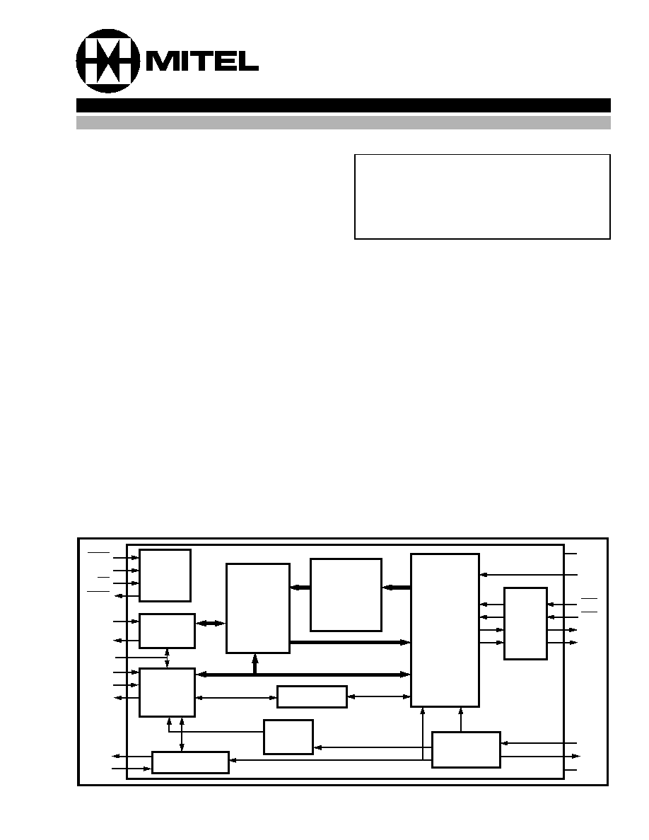
Figure 1 - Functional Block Diagram
V
DD
RxD
RxA
RxB
TxA
TxB
E2i
E8Ko
V
SS
CEPT
Link
Interface
Digital
Attenuator
ROM
ST-BUS
Timing
Circuitry
PCM/Data
Interface
Serial
Control
Interface
ABCD Bit RAM
Control Logic
Phase
Detector
CEPT
Counter
TxMF
C2i
F0i
RxMF
DSTi
DSTo
ADI
CSTi0
CSTi1
CSTo
XCtl
XSt
Remote
&
Digital
Loop-
backs
2 Frame
Elastic Buffer
with Slip
Control
Ordering Information
MT8979AC
28 Pin Ceramic DIP
MT8979AE
28 Pin Plastic DIP
MT8979AP
44 Pin PLCC
-40∞ to 85∞C
ISSUE 7
May 1995
MT8979
CEPT PCM 30/CRC-4 Framer & Interface
ISO-CMOS ST-BUS
TM
FAMILY

MT8979
ISO-CMOS
4-162
Figure 2 - Pin Connections
Pin Description
Pin #
Name
Description
DIP
PLCC
1
2
TxA
Transmit A (Output): A split phase unipolar signal suitable for use with TxB and an
external line driver and transformer to construct the bipolar line signal.
2
3
TxB
Transmit B (Output:) A split phase unipolar signal suitable for use with TxA and an
external line driver and transformer to construct the bipolar line signal.
3
5
DSTo
Data ST-BUS (Output): A 2048 kbit/s serial output stream which contains the 30 PCM or
data channels received from the CEPT line.
4
4
NC
No Connection.
5
9
RxA
Receive A (Input): Received split phase unipolar signal decoded from a bipolar line
receiver.
6
10
RxB
Receive B (Input): Received split phase unipolar signal decoded from a bipolar line
receiver.
7
11
RxD
Received Data (Input): Input of the unipolar data generated from the line receiver. This
data may be NRZ or RZ.
8
13
CSTi1
Control ST-BUS Input #1: A 2048 kbit/s stream that contains channel associated
signalling, frame alignment and diagnostic functions.
9
NC
No Connection.
10
NC
No Connection.
11
17
ADI
Alternate Digit Inversion (Input): If this input is high, the CEPT timeslots which are
specified on CSTi0 as voice channels are ADI coded and decoded. When this bit is low it
disables ADI coding for all channels. This feature allows either ADI or non-ADI codecs to
be used on DSTi and DSTo.
12
19
CSTi0
Control ST-BUS Input #0: A 2048 kbit/s stream that contains 30 per channel control
words and two Master Control Words.
44 PIN PLCC
1
2
3
4
5
6
7
8
9
10
11
12
13
14
15
16
17
18
19
20
28
27
26
25
24
23
22
21
28 PIN CERDIP/PDIP
TxA
TxB
NC
RxA
RxB
RxD
CSTi1
NC
NC
ADI
CSTi0
E8Ko
VSS
VDD
IC
F0i
E2i
NC
RxMF
TxMF
C2i
NC
DSTi
NC
CSTo
XSt
XCtl
DSTo
VSS
DST
o
Tx
B
Tx
A
IC
NC
F0
i
NC
E2
i
NC
RxMF
TxMF
NC
NC
C2i
NC
NC
NC
NC
NC
NC
NC
RxA
RxB
RxD
NC
CSTi1
NC
NC
NC
ADI
VSS
CST
i
0
E8
Ko
NC
VSS
XSt
NC
CST
o
NC
DST
i
XC
t
l
VDD
1
6 5 4 3 2
44 43 42 41 40
7
8
9
10
11
12
13
14
15
16
39
38
37
36
35
34
33
32
31
30
23
18 19 20 21 22
24 25 26 27 28
17
29
NC

ISO-CMOS
MT8979
4-163
13
20
E8Ko
Extracted 8 kHz Clock (Output): An 8 kHz output generated by dividing the extracted
2048 kHz clock by 256 and aligning it with the received CEPT frame. The 8 kHz signal
can be used for synchronizing the system clock to the extracted 2048 kHz clock. Only
valid when device achieves synchronization (goes low during a loss of signal or a loss
of basic frame synchronization condition).
E8Ko goes high impedance when 8kHzSEL = 0 in MCW2.
15
23
XCtl
External Control (Output): An uncommitted external output pin which is set or reset
via bit 1 in Master Control Word 2 on CSTi0. The state of XCtl is updated once per
frame.
16
24
XSt
External Status: The state of this pin is sampled once per frame and the status is
reported in bit 1 of the Master Status Word 1 on CSTo.
17
26
CSTo
Control ST-BUS Output: A 2048 kbit/s serial control stream which provides the 16
signalling words, two Master Status Words, Phase Status Word and CRC Error Count.
18
NC
No Connection.
19
28
DSTi
Data ST-BUS Input: This pin accepts a 2048 kbit/s serial stream which contains the
30 PCM or data channels to be transmitted on the CEPT trunk.
20
NC
No Connection.
21
34
C2i
2048 kbit/s System Clock (Input): The master clock for the ST-BUS section of the
chip. All data on the ST-BUS is clocked in on the falling edge of the C2i and output on
the rising edge. The falling edge of C2i is also used to clock out data on the CEPT
transmit link.
22
37
TxMF
Transmit Multiframe Boundary (Input): This input can be used to set the channel
associated and CRC transmitted multiframe boundary (clear the frame counters). The
device will generate its own multiframe if this pin is held high.
23
38
RxMF
Received Multiframe Boundary (Output): An output pulse delimiting the received
Multiframe boundary. (This multiframe is not related to the received CRC multiframe.)
The next frame output on the data stream (DSTo) is received as frame 0 on the CEPT
link.
24
NC
No Connection.
25
40
E2i
Extracted 2048 kHz Clock (Input): The falling edge of this 2048 kHz clock is used to
latch the received data (RxD). This clock input must be derived from the CEPT
received data and must have its falling edge aligned with the center of the received bit
(RxD).
26
42
F0i
Frame Pulse Input: The ST-BUS frame synchronization signal which defines the
beginning of the 32 channel frame.
27
44
IC
Internal Connection: Tie to V
SS
(Ground) for normal operation.
28
1
V
DD
Positive Power Supply Input (+5 Volts).
14
6,8,
22
V
SS
Negative Power Supply Input (Ground).
Pin Description (Continued)
Pin #
Name
Description
DIP
PLCC
MT8979
ISO-CMOS
4-164
Functional Description
The MT8979 is a CEPT trunk digital link interface
conforming to CCITT Recommendation G.704 for
PCM 30 and I.431 for ISDN. It includes features
such as: insertion and detection of synchronization
patterns, optional cyclical redundancy check and far
end error performance reporting, HDB3 decoding
and optional coding, channel associated or common
channel signalling, programmable digital attenuation
and a two frame received elastic buffer. The
MT8979 can also monitor several conditions on the
CEPT digital trunk, which include, frame and
multiframe synchronization, received all 1's alarms,
data slips as well as framing and CRC errors, both
near and far end.
The system interface to the MT8979 is a TDM bus
structure that operates at 2048 kbit/s known as the
ST-BUS. This serial stream is divided into 125
µ
s
frames that are made up of 32 x 8 bit channels.
The line interface to the MT8979 consists of split
phase unipolar inputs and outputs which are
supplied from/to a bipolar line receiver/driver,
respectively.
CEPT Interface
The CEPT frame format consists of 32, 8 bit
timeslots. Of the 32 timeslots in a frame, 30 are
defined as information channels, timeslots 1-15 and
17-31 which correspond to telephone channels 1-30.
An additional voice/data channel may be obtained by
placing the device in common channel signalling
mode. This allows use of timeslot 16 for 64 kbit/s
common channel signalling.
Synchronization is included within the CEPT bit
stream in the form of a bit pattern inserted into
timeslot 0. The contents of timeslot 0 alternate
between the frame alignment pattern and the
non-frame alignment pattern as described in Figure
4. Bit 1 of the frame alignment and non-frame
alignment bytes have provisions for additional
protection against false synchronization or enhanced
error monitoring. This is described in more detail in
the following section.
In order to accomplish multiframe synchronization, a
16 frame multiframe is defined by sending four zeros
in the high order quartet of timeslot 16 frame 0, i.e.,
once every 16 frames (see Figure 5). The CEPT
format has four signalling bits, A, B, C and D.
Signalling bits for all 30 information channels are
transmitted in timeslot 16 of frames 1 to 15. These
timeslots are subdivided into two quartets (see Table
6).
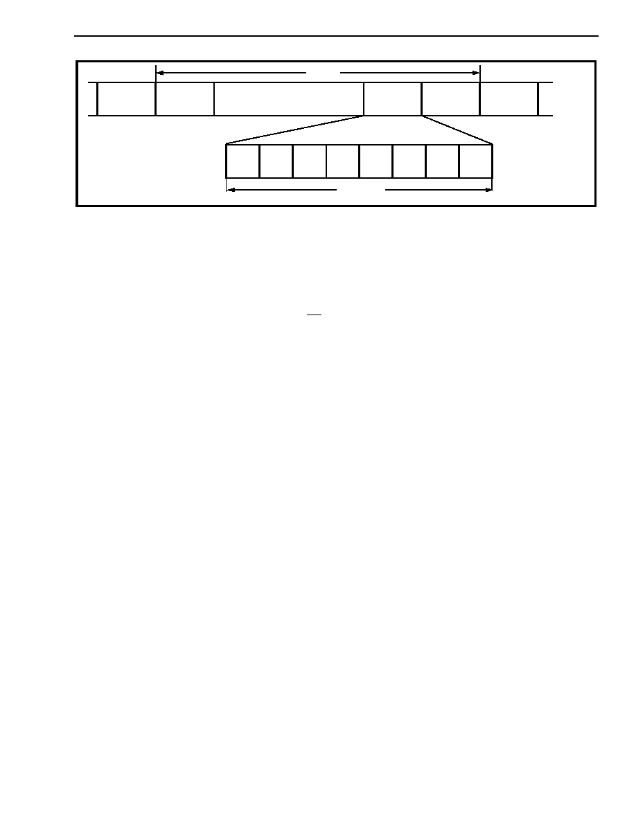
Cyclic Redundancy Check (CRC)
An optional cyclic redundancy check (CRC) has
been incorporated within CEPT bit stream to provide
additional protection against simulation of the frame
alignment signal, and/or where there is a need for an
enhanced error monitoring capability. The CRC
process treats the binary string of ones and zeros
contained in a submultiframe (with CRC bits set to
binary zero) as a single long binary number. This
string of data is first multiplied by x
4
then divided by
the generating polynomial x
4
+x+1. This division
process takes place at both the transmitter and
receiver end of the link. The remainder calculated at
the receiver is compared to the one received with the
data over the link. If they are the same, it is of high
probability that the previous submultiframe was
received error free.
The CRC procedure is based on a 16 frame
multiframe, which is divided into two 8 frame
submultiframes (SMF). The frames which contain
the frame alignment pattern contain the CRC bits, C
1
to C
4
respectively, in the bit 1 position. The frames
Figure 3 - CEPT Link Frame & Multiframe Format
Frame
15
0
14
15
0
Timeslot
0
1
30
31
Most
Significant
Bit (First)
Least
Significant
Bit (Last)
Bit
1
2
3
4
5
6
7
8
Frame
Frame
Frame
Frame
Timeslot
Timeslot
Timeslot
Bit
Bit
Bit
Bit
Bit
Bit
Bit
2.0 ms
(8/2.048)
µ
s
125
µ
s
∑ ∑ ∑ ∑ ∑ ∑ ∑ ∑
∑ ∑ ∑ ∑

ISO-CMOS
MT8979
4-165
which contain the non-frame alignment pattern
contain within the bit 1 position, a 6 bit CRC
multiframe alignment signal and two spare bits (in
frames 13 and 15), which are used for CRC error
performance reporting (refer to Figure 6). During the
CRC encoding procedure the CRC bit positions are
initially set at zero. The remainder of the calculation
is stored and inserted into the respective CRC bits of
the next SMF. The decoding process repeats the
multiplication division process and compares the
remainder with the CRC bits received in the next
SMF.
The two spare bits (denoted Si1 and Si2 in Figure 6)
in the CRC-4 multiframe are used to monitor far-end
error performance. The results of the CRC-4
comparisons for the previously received SMFII and
SMFI are encoded and transmitted back to the far
end in the Si bits (refer to Table 1).
ST-BUS Interface
The ST-BUS is a synchronous time division
multiplexed serial bus with data streams operating at
2048 kbit/s and configured as 32, 64 kbit/s channels
(refer Figure 7). Synchronization of the data transfer
is provided from a frame pulse, which identifies the
frame boundaries and repeats at an 8 kHz rate.
Figure 17 shows how the frame pulse (F0i) defines
the ST-BUS frame boundaries. All data is clocked
into the device on the falling edge of the 2048 kbit/s
clock (C2i), while data is clocked out on the rising
edge of the 2048 kbit/s clock at the start of the bit
cell.
Table 1. Coding of Spare Bits Si1 and Si2
Data Input (DSTi)
The MT8979 receives information channels on the
DSTi pin. Of the 32 available channels on this
serial input, 30 are defined as information channels.
They are channels 1-15 and 17-31. These 30
timeslots are the 30 telephone channels of the CEPT
format numbered 1-15 and 16-30. Timeslot 0 and 16
are unused to allow the synchronization and
signalling information to be inserted, from the Control
Streams (CSTi0 and CSTi1). The relationship
between the input and output ST-BUS stream and
the CEPT line is illustrated in Figures 8 to 12. In
common channel signalling mode timeslot 16
becomes an active channel. In this mode channel 16
on DSTi is transmitted on timeslot 16 of the CEPT
link unaltered. This mode is activated by bit 5 of
channel 31 of CSTi0.
Si1 bit
(frame
13)
Si2 bit
(frame
15)
Meaning
1
1
CRC results for both SMFI, II are
error free.
1
0
CRC result for SMFII is in error.
CRC result for SMFI is error free.
0
1
CRC result for SMFII is error free.
CRC result for SMFI is in error.
0
0
CRC results for both SMFI, II are
in error.
Figure 4 - Allocation of Bits in Timeslot 0 of the CEPT Link
Note 1 : With CRC active, this bit is ignored.
Note 2 : With SiMUX active, this bit transmits SMF CRC results in frames 13 and 15
Note 3 : Reserved for National use
.
Figure 5 - Allocation of Bits in Timeslot 16 of the CEPT Link
Bit Number
1
2
3
4
5
6
7
8
Timeslot 0 containing the
frame alignment signal
Reserved for
International
use
(1)
0
0
1
1
0
1
1
Timeslot 0 containing the
non-frame alignment signal
Reserved for
International
use
(2)
1
Alarm indication to the
remote PCM multiplex
equipment
See
Note
#3
See
Note
#3
See
Note
#3
See
Note
#3
See
Note
#3
Timeslot 16 of frame 0
Timeslot 16 of frame 1
∑ ∑ ∑
Timeslot 16 of frame 15
0000
XYXX
ABCD bits for
telephone
channel 1
(timeslot 1)
ABCD bits for
telephone
channel 16
(timeslot 17)
ABCD bits for
telephone
channel 15
(timeslot 15)
ABCD bits for
telephone
channel 30
(timeslot 31)

MT8979
ISO-CMOS
4-166
Control
Input 0 (CSTi0)
All the necessary control and signalling information
is input through the two control streams. Control
ST-BUS input number 0 (CSTi0) contains the control
information that is associated with each information
channel. Each control channel contains the per
channel digital attenuation information, the individual
loopback control bit, and the voice or data channel
identifier, see Table 2. When a channel is in data
mode (B7 is high) the digital attenuation and
Alternate Digit Inversion are disabled. It should be
noted that the control word for a given information
channel is input one timeslot early, i.e., channel 0 of
CSTi0 controls channel 1 of DSTi. Channels 15 and
31 of CSTi0 contain Master Control Words 1 and 2,
which are used to set up the interface feature as
seen by the respective bit functions of Tables 3 and
4.
Control
Input 1 (CSTi1)
Control ST-BUS input stream number 1 (CSTi1)
contains the synchronization information and the A,
B, C & D signalling bits for insertion into timeslot 16
of the CEPT stream (refer to Tables 5 to 8). Timeslot
0 contains the four zeros of the multiframe alignment
signal plus the XYXX bits (see Figure 5). Channels 1
to 15 of CSTi1 contain the A, B, C & D signalling bits
as defined by the CEPT format (see Figure 5), i.e.,
channel 1 of CSTi1 contains the A,B,C & D bits for
DSTi timeslots 1 and 17. Channel 16 contains the
frame alignment signal, and channel 17 contains the
non-frame alignment signal (see Figure 4). Channel
18 contains the Master Control Word 3 (see Table 9).
Figure 11 shows the relationship between the control
stream (CSTi1) and the CEPT stream.
Control Output (CSTo)
Control ST-BUS output (CSTo) contains the
multiframe signal from timeslot 16 of frame 0 (see
Table 10). Signalling bits A, B, C & D for each CEPT
channel are sourced from timeslot 16 of frames 1-15
and are output in channels 1-15 on CSTo , as shown
in Table 11. The frame alignment signal and
nonframe alignment signal, received from timeslot 0
of alternate frames, are output in timeslots 16 and 17
as shown in Tables 12 and 13.
Channel 18 contains a Master Status Word, which
provides to the user information needed to determine
the operating condition of the CEPT interface i.e.,
frame synchronization, multiframe synchronization,
frame alignment byte errors, slips, alarms, and the
logic of the external status pin (see Table 14). Figure
12, shows the relationship between the control
stream channels and the CEPT signalling channels
in the multiframe. The ERR bit in the Master Status
word is an indicator of the number of errored frame
alignment bytes that have been received in alternate
timeslot zero. The time interval between toggles of
Figure 6 - CRC Bit Allocation and Submultiframing
Note 1 : Remote Alarm. Keep at 0 for normal operation.
Note 2 : Reserved for National use. Keep at 1 for normal operation.
Note 3 : Used to monitor far-end CRC error performance.
Multiple Frame
Component
Frame Type
CRC
Frame #
Timeslot Zero
1
2
3
4
5
6
7
8
Frame Alignment Signal
0
C
1
0
0
1
1
0
1
1
Non-Frame Alignment Signal
1
0
1
A
(1)
Sn
(2)
Sn
(2)
Sn
(2)
Sn
(2)
Sn
(2)
S
Frame Alignment Signal
2
C
2
0
0
1
1
0
1
1
M
Non-Frame Alignment Signal
3
0
1
A
(1)
Sn
(2)
Sn
(2)
Sn
(2)
Sn
(2)
Sn
(2)
F
Frame Alignment Signal
4
C
3
0
0
1
1
0
1
1
Non-Frame Alignment Signal
5
1
1
A
(1)
Sn
(2)
Sn
(2)
Sn
(2)
Sn
(2)
Sn
(2)
I
Frame Alignment Signal
6
C
4
0
0
1
1
0
1
1
Non-Frame Alignment Signal
7
0
1
A
(1)
Sn
(2)
Sn
(2)
Sn
(2)
Sn
(2)
Sn
(2)
Frame Alignment Signal
8
C
1
0
0
1
1
0
1
1
S
Non-Frame Alignment Signal
9
1
1
A
(1)
Sn
(2)
Sn
(2)
Sn
(2)
Sn
(2)
Sn
(2)
M
Frame Alignment Signal
10
C
2
0
0
1
1
0
1
1
F
Non-Frame Alignment Signal
11
1
1
A
(1)
Sn
(2)
Sn
(2)
Sn
(2)
Sn
(2)
Sn
(2)
Frame Alignment Signal
12
C
3
0
0
1
1
0
1
1
I
Non-Frame Alignment Signal
13
Si1
(3)
1
A
(1)
Sn
(2)
Sn
(2)
Sn
(2)
Sn
(2)
Sn
(2)
I
Frame Alignment Signal
14
C
4
0
0
1
1
0
1
1
Non-Frame Alignment Signal
15
Si2
(3)
1
A
(1)
Sn
(2)
Sn
(2)
Sn
(2)
Sn
(2)
Sn
(2)
indicates position of CRC-4
multiframe alignment signal
ISO-CMOS
MT8979
4-167
Figure 7 - ST-BUS Stream Format
CHANNEL
31
0
30
BIT
CHANNEL
CHANNEL
CHANNEL
CHANNEL
31
0
BIT
BIT
BIT
BIT
BIT
BIT
BIT
∑ ∑ ∑
Least
Significant
Bit (Last)
Most
Significant
Bit (First)
(8/2.048)
µ
s
125
µ
s
7
6
5
4
3
2
1
0
the ERR bit can be used to evaluate the bit error
rate of the line according to the CCITT
Recommendation G.732 (see section on Frame
Alignment Error Counter).
Channel 19 contains the Phase Status Word (see
Table 15), which can be used to determine the phase
relationship between the ST-BUS frame pulse (F0i)
and the rising edge of E8Ko. This information could
be used to determine the long term trend of the
received data rate, or to identify the direction of a
slip.
Channel 20 contains the CRC error count (see Table
16). This counter will wrap around once terminal
count is achieved (256 errors). If the maintenance
option is selected (bit 3 of MCW3) the counter is
reset once per second.
Channel 21 contains the Master Status Word 2 (see
Table 17). This byte identifies the status of the CRC
reframe and CRC sync. It also reports the Si bits
received in timeslot 0 of frames 13 and 15 and
the ninth and most significant bit (b
8
) of the 9-bit
Phase Status Word.
Elastic Buffer
The MT8979 has a two frame elastic buffer at the
receiver, which absorbs the jitter and wander in the
received signal. The received data is written into the
elastic buffer with the extracted E2i (2048 kHz) clock
and read out of the buffer on the ST-BUS side with
the system C2i (2048 kHz) clock (e.g., PBX system
clock). Under normal operating conditions, in a
synchronous network, the system C2i clock is
phase-locked to the extracted E2i clock. In this
situation every write operation to the elastic buffer is
followed by a read operation. Therefore, underflow
or overflow of data in the elastic buffer will not occur.
If the system clock is not phase-locked to the
extracted clock (e.g., lower quality link which is not
selected as the clock source for the PBX) then the
data rate at which the data is being written into the
device on the line side may differ from the rate at
which it is being read out on the ST-BUS side.
When the clocks are not phase-locked, two
situations can occur:
Case #1:
If the data on the line side is being written
in at a rate SLOWER than it is being read out on the
ST-BUS side, the distance between the write pointer
and the read pointer will begin to decrease over time.
When the distance is less than two channels, the
buffer will perform a controlled slip which will move
the read pointers to a new location 34 channels
away from the write pointer. This will result in the
REPETITION of the received frame.
Case #2:
If the data on the line side is being written
in at a rate FASTER than it is being read out on the
ST-BUS side, the distance between the write pointer
and the read pointer will begin to increase over time.
When the distance exceeds 42 channels, the elastic
buffer will perform a controlled slip which will move
the read pointer to a new location ten channels away
from the write pointer. This will result in the LOSS of
the last received frame.
Note that when the device performs a controlled slip,
the ST-BUS address pointer is repositioned so that
there is either a 10 channel or 34 channel delay
between the input CEPT frame and the output
ST-BUS frame. Since the buffer performs a
controlled slip only if the delay exceeds 42 channels
or is less than two channels, there is a minimum
eight channel hysteresis built into the slip
mechanism. The device can, therefore, absorb eight
channels or 32.5µs of jitter in the received signal.
There is no loss of frame synchronization, multiframe
synchronization or any errors in the signalling bits
when the device performs a slip.

MT8979
ISO-CMOS
4-168
Fi
g
u
r
e
8
-
R
e
l
a
t
i
o
n
s
h
i
p
b
e
t
w
e
e
n I
n
put
D
S
T
i
C
h
a
n
n
e
l
s
a
nd
T
r
a
n
s
m
i
t
t
e
d C
E
P
T
T
i
m
e
s
l
ot
s
Fi
gur
e
9
-
R
e
l
a
t
i
ons
hi
p
be
t
w
e
e
n R
e
c
e
i
v
e
d
C
E
P
T
T
i
m
e
s
l
o
t
s
a
nd
Out
p
u
t
D
S
T
o
C
h
a
n
ne
l
s
Fi
g
u
r
e
1
0
-
R
e
l
a
t
i
ons
hi
p be
t
w
e
e
n
I
n
p
u
t
C
S
T
i
0
C
h
a
n
ne
l
s
a
n
d
C
ont
r
o
l
l
e
d C
E
P
T
T
i
m
e
s
l
ot
s
Fi
g
u
r
e
1
1
-
R
e
l
a
t
i
o
n
s
h
i
p
b
e
t
w
e
e
n I
n
pu
t
C
S
Ti
1
C
h
a
n
n
e
l
s
a
n
d T
r
a
n
s
m
i
t
t
e
d C
E
P
T
F
r
a
m
e
s
F
i
gur
e
1
2
-
R
e
l
a
t
i
on
s
h
i
p
b
e
t
w
e
e
n
R
e
c
e
i
v
e
d C
E
P
T
Fra
m
e
s
a
nd O
u
t
p
u
t
C
S
T
o
C
h
a
n
ne
l
s
-
*
D
e
n
o
t
e
s
U
n
us
ed
C
h
an
ne
l (
C
S
T
o
ou
tpu
t
i
s
no
t p
u
t
in
h
i
g
h
i
m
pe
da
nc
e
sta
t
e
)
-
CCS
D
e
no
t
e
s S
i
gn
al
li
ng
C
h
an
ne
l i
f
C
o
mmo
n C
h
a
n
n
e
l
S
i
gn
al
l
i
n
g
Mo
de
S
e
le
ct
ed
-
A
D
e
no
tes
F
r
am
e
-
A
l
i
g
n
m
en
t Fr
am
e
-
S1
D
e
no
te
s Ma
st
er
S
t
a
t
u
s
W
o
r
d
1 (
M
S
W
1)
-
N
D
e
no
tes
N
o
n
Fr
a
m
e
-
A
l
ig
nm
en
t F
r
am
e
-
S2
D
e
no
te
s P
h
a
s
e S
t
at
us
W
o
r
d
(
P
S
W
)
-
C1
,
C2
,
C3
D
e
no
te
s
Ma
st
er
C
o
n
t
r
o
l
W
o
r
d
s
1
,
2,
3
-
S3
De
n
o
t
e
s
CRC
E
rro
r Co
u
n
t
-
SIG
D
e
n
o
t
e
s
S
i
gn
al
li
ng
C
h
a
nne
l
-
S4
D
e
no
te
s Ma
st
er
S
t
a
t
u
s
W
o
r
d
2 (
M
S
W
2)
D
S
Ti
C
h
a
nne
l #
0
1
2
3
4
5
6
7
8
9
10
1
1
12
1
3
14
1
5
16
17
1
8
19
2
0
21
2
2
23
2
4
25
26
2
7
28
2
9
30
3
1
CEPT
Tim
e
s
lot #
12
34
567
89
1
0
1
1
1
2
1
3
1
4
1
5
CCS
17
1
8
19
2
0
21
2
2
23
2
4
25
26
2
7
28
2
9
30
3
1
D
S
Ti
C
h
a
nne
l #
0
1
2
3
4
5
6
7
8
9
10
1
1
12
1
3
14
1
5
16
17
1
8
19
2
0
21
2
2
23
2
4
25
26
2
7
28
2
9
30
3
1
CEPT
Tim
e
s
lot #
0
1
2
3
4
5
6
7
8
9
10
1
1
12
1
3
14
1
5
SI
G
17
1
8
19
2
0
21
2
2
23
2
4
25
26
2
7
28
2
9
30
3
1
CS
T
i
0
C
h
a
nne
l #
01
23456789
1
0
1
1
1
2
1
3
1
4
1
5
1
6
1
7
1
8
1
9
2
0
2
1
2
2
2
3
2
4
2
5
2
6
2
7
2
8
2
9
3
0
3
1
D
e
vi
ce
C
o
n
t
r
o
l
C1
C2
C
E
P
T
C
h
an
ne
l
#
C
o
ntr
o
l
Wor
d
12
3456789
1
0
1
1
1
2
1
3
1
4
1
5
1
7
1
8
1
9
2
0
2
1
2
2
2
3
2
4
2
5
2
6
2
7
2
8
2
9
3
0
3
1
C
S
Ti1
Ch
a
n
n
e
l
#
0
1
2
3
4
5
6
7
8
9
1
0
1
1
12
1
3
14
1
5
16
1
7
1
8
19
2
0
21
2
2
23
24
2
5
26
2
7
28
29
3
0
31
De
v
i
c
e
Co
n
t
ro
l
C
3
**
***
**
**
***
*
CE
PT
F
RAM
E #
CHANNEL
#
0
16
1
16
2
16
3
16
4
16
5
16
6
16
7
16
8
16
9
16
10
16
11
16
12
16
13
16
14
16
15
16
A
0
N
0
CS
T
o
Ch
a
n
n
e
l
#
0
1
2
3
4
5
6
7
8
9
10
1
1
12
1
3
14
1
5
16
1
7
18
1
9
20
2
1
22
2
3
24
2
5
26
2
7
28
2
9
30
3
1
De
v
i
c
e
Sta
tus
S
1
S
2
S
3
S
4
**
**
**
**
**
CEP
T
F
RAM
E #
T
I
M
ESL
O
T
#
0
16
1
16
2
16
3
16
4
16
5
16
6
16
7
16
8
16
9
16
10
16
11
16
12
16
13
16
14
16
15
16
A
0
N
0

ISO-CMOS
MT8979
4-169
Frame Alignment Error Counter
The MT8979 provides an indication of the bit error
rate found on the link as required by CCITT
Recommendation G.703. The ERR bit (Bit 5 of
MSW1) is used to count the number of errors found
in the frame alignment signal and this can be used to
estimate the bit error rate. The ERR bit changes
state when 16 errors have been detected in the
frame alignment signal. This bit can not change state
more than once every 128 ms, placing an upper limit
on the detectable error rate at approximately 10
-3
.
The following formula can be used to calculate the
BER:
where:
7 - is the number of bits in the frame alignment
signal (0011011).
16 - is the number of errored frame alignment
signals counted between changes of state
of the ERR bit.
4000 - is the number of frame alignment signals in
a one second interval.
This formula provides a good approximation of the
BER given the following assumptions:
1.
The bit errors are uniformly distributed on the
line. In other words, every bit in every channel is
equally likely to get an error.
2.
The errors that occur in channel 0 are bit errors.
If the first assumption holds and the bit error rate
is reasonable, (below 10
-3
) then the probability of
two or more errors in seven bits is very low.
Attenuation ROM
All transmit and receive data in the MT8979 is
passed through the digital attenuation ROM
according to the values set on bits 5 - 0 of data
channels in the control stream (CSTi0). Data can be
attenuated on a per-channel basis from 1 to -6 dB for
both Tx and Rx data (refer Table 2).
Digital attenuation is applied on a per-channel basis
to the data found one channel after the control
information stored in the control channel CSTi0, i.e.,
control stream 0 channel 4 contains the attenuation
setting for data stream (DSTo) channel 5.
BER=
16* number of times ERR bit toggles
7 * 4000 * elapsed time in seconds
Signalling Bit RAM
The A, B, C, & D Bit RAM is used to retain the status
of the per-channel signalling bits so that they may be
multiplexed into the Control Output Stream (CSTo).
This signalling information is only valid when the
module is synchronized to the received data stream.
If synchronization is lost, the status of the signalling
bits will be retained for 6.0 ms provided the signalling
debounce is active.
Integrated into the signalling bit RAM is a debounce
circuit which will delay valid signalling bit changes for
6.0 to 8.0 ms. By debouncing the signalling bits, a
bit error will not affect the call in progress. (See Table
3, bits 3-0 of channel 15 on the CSTi0 line.)
CEPT PCM 30 Format MUX
The CEPT Link Multiplexer formats the data stream
corresponding to the CEPT PCM 30 format. This
implies that the multiplexer will use timeslots 1 to 15
and 17 to 31 for data and uses timeslots 0 & 16 for
the synchronization and channel associated
signalling.
The frame alignment or non-frame alignment signals
for timeslot zero are sourced by the control stream
input CSTi1 channel 16 and 17, respectively. The
most significant bit of timeslot zero will optionally
contain the cyclical redundancy check, CRC
multiframe pattern and Si bits used for far-end CRC
monitoring.
Framing Algorithms
There are three distinct framers within the MT8979.
These include a frame alignment signal framer, a
multiframe framer and a CRC framer. Figure 13
shows the state diagram of the framing algorithms.
The dotted lines shows optional features, which are
enabled in the maintenance mode.
The frame synchronization circuit searches for the
first frame alignment signal within the bit stream.
Once detected, the frame counters are set to find the
non-frame alignment signal. If bit 2 of the non-frame
alignment signal is not one, a new search is initiated,
else the framer will monitor for the frame alignment
in the next frame. If the frame alignment signal is
found, the device immediately declares frame
synchronization.

MT8979
ISO-CMOS
4-170
The multiframe synchronization algorithm is
dependent upon the state of frame alignment framer.
The multiframe framer will not initiate a search for
multiframe synchronization until frame sync is
achieved. Multiframe synchronization will be
declared on the first occurrence of four consecutive
zeros in the higher order quartet of channel 16.
Once multiframe synchronization is achieved, the
framer will only go out of synchronization after
detection of two errors in the multiframe signal or
loss of frame alignment synchronization.
The CRC synchronization algorithm is also
dependent on the state of the frame alignment
framer, but is independent of the multiframe
synchronization. The CRC framer will not initate a
search for CRC framing signal until frame alignment
synchronization is achieved. Once frame alignment
synchronization is acquired, the CRC framer must
find two framing signals in bit 1 of the non-frame
alignment signal. Upon detection of the second CRC
framing signal the MT8979 will immediately go into
CRC synchronization. When maintenance feature is
enabled (maint bit = 1) the CRC framer will force a
complete reframe of the device if CRC frame
synchronization is not found within 8 ms or more
than 914 CRC errors occur per second.
Figure 13 - Synchronization State Diagram
out of
synchronization
search for frame
alignment
signal
verify bit 2 of non-
frame alignment
signal
verify second
occurrence of frame
alignment signal
find two CRC
frame alignment
CRC synchronization
acquired
search for
multiframe align-
ment signal
multiframe synchro-
nization acquired
check for two errored
multiframe alignment
signals
No
No
Yes
Yes
Yes
Yes
Yes
Yes
No
# of consecutive incorrect
frame alignment signals = 3
time out > 8ms
No
- - - - - Only if the
maintenance
option is
selected
signals
No
number of CRC
errors > 914/s
frame synchroni-
zation acquired

ISO-CMOS
MT8979
4-171
Table 2. Per Channel Control Word: Data Format for CSTi0 Channels 0-14, and 16-30
Table 3. Master Control 1 (MCW1): Data Format for CSTi0 Channel 15
BIT
NAME
DESCRIPTION
7
DATA
Data Channel: If `1`, then the controlled timeslot on the CEPT 2048 kbit/s link is
treated as a data channel; i.e., no ADI encoding or decoding is performed on
transmission or reception, and digital attenuation is disabled.
If `0`, then the state of the ADI pin determines whether or not ADI encoding and
decoding is performed.
6
LOOP
Per-Channel Loopback: If `1`, then the controlled timeslot on the transmitted
CEPT 2048 kbit/s link is looped internally to replace the data on the corresponding
received timeslot. If `0`, then this function is disabled.
This function only operates if frame synchronization is received from the CEPT link.
If more than one channel is looped per frame only the first one will be active.
5,4,3
RXPAD4,2,1
Receive Attenuation Pad: Per timeslot receive attenuation control bits.
RXPAD4
0
0
0
0
1
1
1
1
RXPAD2
0
0
1
1
0
0
1
1
RXPAD1
0
1
0
1
0
1
0
1
Gain (dB)
0
-1
-2
-3
-4
-5
-6
1
2,1,0
TXPAD4,2,1
Transmit Attenuation Pad: Per timeslot transmit attenuation control bits.
TXPAD4
0
0
0
0
1
1
1
1
TXPAD2
0
0
1
1
0
0
1
1
TXPAD1
0
1
0
1
0
1
0
1
Gain (dB)
0
-1
-2
-3
-4
-5
-6
1
BIT
NAME
DESCRIPTION
7
(N/A)
Keep at `1` for normal operation.
6
LOOP16
Channel 16 Loopback: If `1`, then timeslot 16 on the transmitted CEPT 2048 kbit/s link
is looped internally to replace the data received on timeslot 16.
If `0,` then this function is disabled.
This function only operates if frame synchronization is received from the CEPT link and
only a single timeslot can be looped within the frame.
5,4
(N/A)
Keep at `1` for normal operation.
3,2,
1
& 0
NDBD, NDBC,
NDBB
& NDBA
Signalling Bit Debounce: If `1`, then no debouncing is applied to the received A, B, C or
D signalling bits. If `0`, then the received A, B, C or D signalling bits are debounced for
between 6 and 8 ms.

MT8979
ISO-CMOS
4-172
Table 4. Master Control 2 (MCW2): Data Format for CSTi0 Channel 31
Table 5. Multiframe Alignment Signal: Data Format for CSTi1 Channel 0
on the Transmitted CEPT Link
BIT
NAME
DESCRIPTION
7
(N/A)
Keep at `1` for normal operation.
6
(N/A)
Keep at `0` for normal operation.
5
CCS
Common Channel Signalling: If 1, then the MT8979 operates in its common channel
signalling mode. Channel 16 on the DSTi pin is transmitted on timeslot 16 of the CEPT
link, and timeslot 16 from the received CEPT link is output on channel 16 on the DSTo
pin. Channel 15 on the CSTi0 pin contains the information for the control of timeslot 16.
Channels 0 to 15 on CSTi1 and CSTo are unused.
If `0`, the device is in channel associated signalling mode where channel 16 is used to
transmit the ABCD signalling bits.
4
8KHzSEL
8KHz Select: If `1`, then an 8 kHz signal synchronized to the received CEPT 2048 kbit/s
link is output on the E8Ko pin. This feature is only valid when frame synchronization is
received from the CEPT link.
If `0`, then the E8Ko pin goes into its high impedance state.
3
TXAIS
Transmit Alarm Indication Signal:
If `1`, then an all 1' s alarm signal is transmitted on all timeslots.
If `0`, then the timeslots functions normally.
2
TXTS16AIS
Transmit Timeslot 16 Alarm Indication Signal:
If `1`, then an all 1's alarm signal is transmitted on timeslot 16.
If `0`, then timeslot 16 functions normally.
1
XCTL
External Control:
If `1`, then the XCtl pin is driven high.
If `0`, then the XCtl pin is driven low.
0
(N/A)
(unused)
BIT
NAME
DESCRIPTION
7-4
MA1-4
Transmit Multiframe Alignment Bits 1 to 4: These bits are transmitted on the CEPT
2048 kbit/s link in bit positions 1 to 4 of timeslot 16 of frame 0 of the multiframe. They
should be kept at `0` to allow multiframe alignment to be detected.
3
X1
This bit is transmitted on the CEPT 2048 kbit/s link in bit position 5 of timeslot 16 of
frame 0 of the multiframe. It is a spare bit which should be kept at `1` if unused.
2
Y
This bit is transmitted on the CEPT 2048 kbit/s link in bit position 6 of timeslot 16 of
frame 0 of the multiframe. It is used to indicate the loss of multiframe alignment to the
remote end of the link. A `1` on this bit is the signal that multiframe alignment on the
received link has been lost. A `0' indicates that multiframe alignment is detected.
1,0
X2,X3
These bits are transmitted on the CEPT 2048 kbit/s link in bit positions 7 and 8
respectively, of timeslot 16 of frame 0 of the multiframe. They are spare bits which
should be kept at `1` if unused.

ISO-CMOS
MT8979
4-173
Table 6. Channel Associated Signalling: Data Format for CSTi1 Channels 1 to 15
Table 7. Frame Alignment Signal: Data Format for CSTi1 Channel 16
BIT
NAME
DESCRIPTION
7,
6,
5
& 4
A(N),
B(N),
C(N)
& D(N)
Transmit Signalling Bits for Channel N: These bits are transmitted on the CEPT 2048
kbit/s link in bit positions 1 to 4 of timeslot 16 in frame N, and are the A, B, C and D
signalling bits associated with telephone channel N. The value of N lies in the range 1 to
15 and refers to the channel on the CSTi1 channel from which the bits are sourced, the
telephone channel with which the bits are associated and the frame on the CEPT link on
which the bits are transmitted. For example, the bits input on the CSTi1 pin on channel 3
are associated with telephone channel 3, which is timeslot 3 of the CEPT link, and are
transmitted on bits positions 1 to 4 of timeslot 16 in frame 3 of each multiframe on the
CEPT link . If bits B, C or D are not used they should be given the values `1, 0` and `1`
respectively. The combination `0000` for ABCD bits should not be used for telephone
channels 1 to 15 as this would interfere with multiframe alignment.
3,
2,
1
& 0
A(N+15),
B(N+15),
C(N+15)
& D(N+15)
Transmit Signalling Bits for Channel N+15: These bits are transmitted on the CEPT
2048 kbit/s link in bit positions 5 to 8 of timeslot 16 in frame N, and are the A, B, C and D
signalling bits associated with telephone channel N+15. The value of N lies in the range 1
to 15 and refers to both the channel on the CSTi1 stream where the bits are supplied and
the frame on the CEPT link on which the bits are transmitted, and indirectly indicates the
telephone channel with which the bits are are associated. For example, the bits input on
the CSTi1 pin on channel 3 are associated with telephone channel 18, which is timeslot 19
of the CEPT link, and are transmitted in bits positions 5 to 8 of timeslot 16 in frame 3 of
each multiframe on the CEPT link .
BIT
NAME
DESCRIPTION
7
IU0
International Use 0: When CRC is disabled, this bit is transmitted on the CEPT 2048
kbit/s link in bit position 1 of timeslot 0 of frame-alignment frames . It is reserved for
international use and should be kept at `1' when not used. If CRC is enabled, this bit is not
used.
6-0
FAF2-8
Transmit Frame Alignment Frame Bits 2 to 8: These bits are transmitted on the CEPT
2048 kbit/s link in bit positions 2 to 8 of timeslot 0 of frame-alignment frames. These bits
form the frame alignment signal and should be set to `0011011`.

MT8979
ISO-CMOS
4-174
Table 8. Non-Frame-Alignment Signal: Data Format for CSTi1 Channel 17
Table 9. Master Control Word 3 (MCW3): Data Format for CSTi1 Channel 18
BIT
NAME
DESCRIPTION
7
IU1
International Use 1: When the CRC is disabled and SiMUX bit in MCW3 is disabled, this
bit is transmitted on the CEPT 2048 kbit/s link in bit position 1 of timeslot 0 of
non-frame-alignment frames . It is reserved for international use and should be kept at `1`
when not used. If CRC is enabled and SiMUX is disabled, this bit is transmitted in bit 1 of
timeslot 0 for frame 13 and 15. If both CRC and SiMUX are enabled, then this bit is not
used.
6
NFAF
Transmit Non-Frame Alignment Bit: This bit is transmitted on the CEPT 2048 kbit/s link
in bit position 2 of timeslot 0 of non-frame-alignment frames. In order to differentiate
between frame-alignment frames and non-frame-alignment frames, this bit should be kept
at `1`.
5
ALM
Non-Frame Alignment Alarm: This bit is transmitted on the CEPT 2048 kbit/s link in bit
position 3 of timeslot 0 of non-frame-alignment frames . It is used to signal an alarm to the
remote end of the CEPT link. The bit should be set to `1` to signal an alarm and should be
kept at `0` under normal operation.
4-0
NU1-5
National Use: These bits are transmitted on the CEPT 2048 kbit/s link in bit positions 4 to
8 of timeslot 0 of non-frame-alignment frames . These bits are reserved for national use,
and on crossing international borders they should be set to `1`.
BIT
NAME
DESCRIPTION
7
N/A
Keep at zero for normal operation.
6
SiMUX
When set to `1', this bit will cause the SMFI CRC result to be transmitted in the next
outgoing Si1 bit in frame 13 and the SMFII CRC result to be transmitted in the next
outgoing Si2 bit in frame 15.
5
RMLOOP
Remote Loopback: If set the RxA
and RxB
signals are looped to TxB and TxA
respectively.
4
HDB3en
Enable HDB3 Encoding: A '1' will disable the HDB3 line coding and transmit the
information transparently.
3
Maint
Maintenance: A '1' will force a terminal reframe if the CRC multiframe synchro- nization
is not achieved within 8 ms of frame synchronization. Reframe will also be generated if
more than 914 CRC errors occur within a one second interval (CRC error counter is reset
with every one second interval). A '0' will disable this option.
2
CRCen
Enable Cyclical Redundancy Check: A '1' will enable the CRC generation on the
transmit data. A '0' will disable the CRC generator. The CRC receiver is always active
regardless of the state of CRCen.
1
DGLOOP
Digital Loopack: When set, the transmitted signal is looped around from DSTi to DSTo.
The normal received data is interrupted.
0
ReFR
Force Reframe: If set, for at least 1 frame, and then cleared the chip will begin to search
for a new frame position when the chip detects the change in state from high to low. Only
the change from high to low will cause a reframe, not a continuous low level.

ISO-CMOS
MT8979
4-175
Table 10. Received Multiframe Alignment Signal: Data Format for CSTo Channel 0
Table 11. Received Channel Associated Signalling: Data Format for CSTo Channels 1 to 15
Table 12. Received Frame Alignment Signal: Data Format for CSTo Channel 16
BIT
NAME
DESCRIPTION
7-4
MA1-4
Receive Multiframe Alignment Bits 1 to 4: These are the bits which are received
from the CEPT 2048 kbit/s link in bit positions 1 to 4 of timeslot 16 of frame 0 of the
multiframe. They should all be `0`.
3
X1
This is the bit which is received on the CEPT 2048 kbit/s link in bit position 5 of
timeslot 16 of frame 0 of the multiframe. It is a spare bit which should be `1` if unused.
It is not debounced.
2
Y
This is the bit which is received on the CEPT 2048 kbit/s link in bit position 6 of
timeslot 16 of frame 0 of the multiframe. It is used to indicate the loss of multiframe
alignment at the remote end of the link. A `1` on this bit is the signal that multiframe
alignment at the remote end of the link has been lost. A `0` indicates that multiframe
alignment is detected. It is not debounced.
1,0
X2,X3
These are the bits which are received on the CEPT 2048 kbit/s link in bit positions 7
and 8 respectively, of timeslot 16 of frame 0 of the multiframe. They are spare bits
which should be `1` if unused. They are not debounced.
BIT
NAME
DESCRIPTION
7,
6,
5
& 4
A(N),
B(N),
C(N)
& D(N)
Receive Signalling Bits for Channel N: These are the bits which are received from the
CEPT 2048 kbit/s link in bit positions 1 to 4 of timeslot 16 in frame N (frame #), and are the
A, B, C and D signalling bits associated with telephone channel N. The value of N lies in
the range 1 to 15 and refers to the channel on the CSTo stream on which the bits are
output, the telephone channel with which the bits are associated and the frame on the
CEPT link on which the bits are received. For example, the bits output on the CSTo
stream on channel 3 are associated with telephone channel 3, which is timeslot 3 of the
CEPT link, and are received on bits positions 1 to 4 of timeslot 16 in frame 3 of each
multiframe on the CEPT link . If bits B, C or D are not used they should have the values `1,
0` and `1` respectively. The combination `0000` for ABCD bits should not be found for
telephone channels 1 to 15 as this implies interference with multiframe alignment.
3,
2,
1
& 0
A(N+15),
B(N+15),
C(N+15)
& D(N+15)
Receive Signalling Bits for Channel N+ 15: These are the bits which are received from
the CEPT 2048 kbit/s link in bit positions 5 to 8 of timeslot 16 in frame N, and are the A, B,
C and D signalling bits associated with telephone channel N+15. The value of N lies in the
range 1 to 15 and refers to both the channel on the CSTo stream where the bits are output
and the frame on the CEPT link on which the bits are received, and indirectly indicates the
telephone channel with which the bits are are associated. The associated channel is
N+15.
For example, the bits output on the CSTo stream on channel 3 are associated with
telephone channel 18, which is timeslot 19 of the CEPT link, and are received on bits
positions 5 to 8 of timeslot 16 in frame 3 of each multiframe on the CEPT link .
BIT
NAME
DESCRIPTION
7
IU0
International Use 0: This is the bit which is received from the CEPT 2048 kbit/s link in bit
position 1 of timeslot 0 of frame-alignment frames . It is reserved for the CRC remainder or
for international use.
6-0
FAF2-8
Frame Alignment Signal Bits 2 to 8: These are the bits which are received from the
CEPT 2048 kbit/s link in bit positions 2 to 8 of timeslot 0 of frame-alignment frames.
These bits form the frame alignment signal and should have the values of `0011011`.

MT8979
ISO-CMOS
4-176
Table 13. Received Non-Frame Alignment Signal: Data Format for CSTo Channel 17
Table 14. Master Status Word 1 (MSW1): Data Format for CSTo Channel 18
Table 15. Phase Status Word (PSW): Data Format for CSTo Channel 19
BIT
NAME
DESCRIPTION
7
IU1
International Use 1: This is the bit which is received from the CEPT 2048 kbit/s link in
bit position 1 of timeslot 0 of non-frame-alignment frames . It is reserved for the CRC
framing or as international bits.
6
NFAF
Receive Non-Frame Alignment Bit: This is the bit which is received from the CEPT
2048 kbit/s link in bit position 2 of timeslot 0 of non-frame-alignment frames . This bit
should be `1` in order to differentiate between frame-alignment frames and
non-frame-alignment frames.
5
ALM
Non-Frame Alignment Alarm: This is the bit which is received from the CEPT 2048
kbit/s link in bit position 3 of timeslot 0 of non-frame-alignment frames . It is used to signal
an alarm from the remote end of the CEPT link. This bit should have the value `0` under
normal operation and should go to `1 `to signal an alarm.
4-0
NU1-5
National Use: These are the bits which are received on the CEPT 2048 kbit/s link in bit
positions 4 to 8 of timeslot 0 of non-frame-alignment frames . These bits are reserved for
national use, and on crossing international borders they should have the value `1`.
BIT
NAME
DESCRIPTION
7
TFSYN
Frame Sync: This bit goes to `1` to indicate a loss of frame alignment synchronization by
the MT8979. It goes to `0` when frame synchronization is detected.
6
MFSYN
Multiframe Sync: This bit goes to `1` to indicate a loss of multiframe synchronization by
the MT8979. It goes to `0` when multiframe synchronization is detected.
5
ERR
Frame Alignment Error: This bit changes state when 16 or more errors have been
detected in the frame alignment signal. It will not change state more than once every 128
ms.
4
SLIP
Control Slip: This bit changes state when a slip occurs between the received CEPT
2048 kbit/s link and the 2048 kbit/s ST-BUS.
3
RXAIS
Receive Alarm Indication Signal: This bit goes to `1` to signal that an all-ones alarm
signal has been detected on the received CEPT 2048 kbit/s . It goes to '0' when the
all-ones alarm signal is removed.
2
RXTS16AIS
Receive Timeslot 16 Alarm Indication Signal: This bit goes to `1` to signal that an
all-ones alarm signal has been detected on channel 16 of the received CEPT 2048 kbit/s
link. It goes to '0' when the all-ones alarm signal is removed.
1
XS
External Status: This bit contains the data sampled once per frame at the XS pin.
0
N/A
(Unused).
BIT
NAME
DESCRIPTION
7 - 3
TxTSC
Transmit Timeslot Count: The value of these five bits indicate the timeslot count
between the ST-BUS frame pulse and the rising edge of E8Ko.
2 - 0
TxBTC
Transmit Bit Count:The value of these three bits indicate the bit position within the
timeslot count reported in TxTSC above.

ISO-CMOS
MT8979
4-177
Table 16. CRC Error Count: Data Format for CSTo Channel 20
Table 17. Master Status Word 2 (MSW2): Data Format for CSTo Channel 21
BIT
NAME
DESCRIPTION
7 - 0
CERC
CRC Error Counter: This byte is the CRC error counter. The counter will wrap around
once it reaches FF count. If maintenance option is activated, the counter will reset after a
one second interval.
BIT
NAME
DESCRIPTION
7
Si2
The received Si bit in frame 15 is reported in this bit. Si2 will be updated after each
RxMF pulse (pin 23).
6
Si1
The received Si bit in frame 13 is reported in this bit. Si1 will be updated after each
RxMF pulse (pin 23).
5-4
NA
Unused.
3
CRCTimer
CRC Timer: Transition from 1 to 0 indicates the start of one second interval in which
CRC errors are accumulated. This bit stays high for 8 ms.
2
CRCRef
CRC Reframe: A '1' indicates that the receive CRC multiframe synchronization could
not be found within the time out period of 8 ms after detecting frame synchronization.
This bit will go low if CRCSync goes low or if Maintenance is not activated.
1
CRCSync
CRC Sync: A '0' indicates that CRC multiframing has been detected.
0
FrmPhase
Frame Count: This is the ninth and most significant bit (b8) of the Phase Status Word
(see Table 15). If the phase status word is incrementing, this bit will toggle when the
phase reading exceeds ST-BUS channel 31, bit 7. If the phase word is decrementing,
then this bit will toggle when the reading goes below ST-BUS channel 0, bit 0.
Applications
The MT8979 is only a link interface to the CEPT
trunk. As such, an external line driver and receiver is
required along with an appropriate pulse transformer
before being connected to the line.
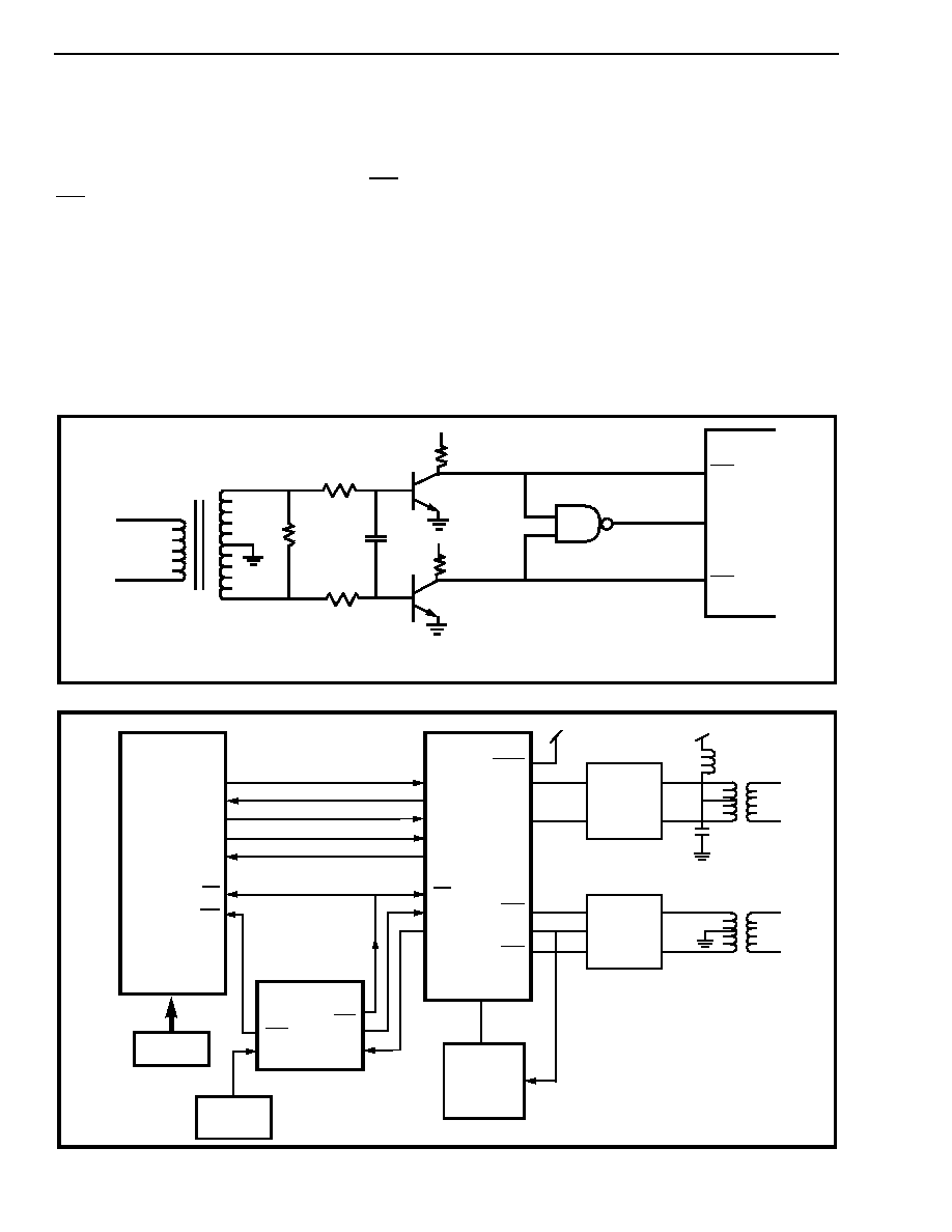
Transmitter
In order to generate a bipolar line signal, the link
interface to the MT8979 provides the user with two
bipolar steering outputs, TxA and TxB. These
correspond to the required positive and negative
pulses on the transmission line. Figure 14 shows a
recommended output circuit for driving a line pulse
transformer.
The transistors are driven into saturation when they
are turned on, which applies a step function to the
transformer. The step input to the transformer
produces a nearly constant di/dt before the current
reaches steady state. By operating in the transient
portion of the inductance response, the secondary of
the transformer produces an almost square pulse.
The base terminal of the transistors is AC coupled to
the MT8979 so that there is no DC path from V
DD
to
ground.
Figure 14 - Bipolar Line Driver
TxA
TxB
MT8979
∑
∑
∑
∑
∑
∑
∑
∑
∑
+12V
33
µ
H
47µ
F
∑
TIPo
RINGo
:.5
1.:
1.:
MT8979
ISO-CMOS
4-178
Receiver
The receive line interface circuit shown in Figure 15
will decode the HDB3 line signals into two split
phase unipolar steering signals. These signals
are used to drive the violation detectors RxA and
RxB as well as being NAND`ed to produce the
received data (RxD).
The NAND gate was removed from the devices to
make the delay for the data path equal to the delay
of the clock path. This will optimize the jitter
performance of the receiver.
The typical connection diagram for the CEPT digital
trunk interface is provided in Figure 16. The
bipolar line driver and receiver have been simplified
for convenience as well as the addition of a clock
extractor and phase-lock loop. The clock extractor is
required to adjust the phase of the E2 clock in order
to sample the received data in the middle of the
pulse on RxD. The phase-lock loop, on the other
hand, will correct the system clocks to absorb the
low rate wander present on the line.
Please note: The configuration shown in Figure 16
using the MT8940 may not meet some international
standards for jitter performance. In cases where
strict idle jitter specifications must be met, a custom
phase-lock loop may be required.
Figure 15 - Typical Bipolar Line Receiver
Figure 16 - Typical Connection Diagram
RxT
RxR
RxA
RxD
RxB
MT8979
1:
:1
:1
+5V
+5V
74LS00
∑
∑
∑
∑
∑
∑
∑
∑
MT8979
DSTi
DSTo
CSTo0
CSTi1
CSTo
F0i
C2i
E8Ko
TxMF
TxA
TxB
RxA
RxD
RxB
Line
Driver
Line
Receiver
Clock
Extractor
16.388
Crystal
MT8980
STo0
STi0
STo1
STo2
STi1
F0i
C4i
µ
P
MT8940
C4b
F0b
V
DD
V
DD
∑
∑
E2i

ISO-CMOS
MT8979
4-179
* Exceeding these values may cause permanent damage. Functional operation under these conditions is not implied.
Typical figures are at 25∞C and are for design aid only: not guaranteed and not subject to production testing.
Characteristics are for clocked operation over the ranges of recommended operating temperature and supply voltage.
Typical figures are at 25∞C and are for design aid only: not guaranteed and not subject to production testing.
Typical figures are at 25∞C and are for design aid only: not guaranteed and not subject to production testing.
Absolute Maximum Ratings*
- Voltages are with respect to ground (V
SS
) unless otherwise stated.
Parameter
Symbol
Min
Max
Units
1
Supply Voltage
V
DD
-0.3
7
V
2
Voltage at Digital Inputs
V
I
-0.3
V
DD
+ 0.3
V
3
Current at Digital Inputs
I
I
30
mA
4
Voltage at Digital Outputs
V
O
-0.3
V
DD
+ 0.3
V
5
Current at Digital Outputs
I
O
30
mA
6
Storage Temperature
T
ST
-65
150
∞C
7
Package Power Dissipation
P
800
mW
Recommended Operating Conditions
- Voltages are with respect to ground (V
SS
) unless otherwise stated.
Characteristics
Sym
Min
Typ
Max
Units
Test Conditions
1
Operating Temperature
T
OP
-40
85
∞C
2
Supply Voltage
V
DD
4.5
5
5.5
V
3
Input Voltage High
V
H
2.4
V
DD
V
For 400 mV noise margin
4
Input Voltage Low
V
L
V
SS
0.4
V
For 400 mV noise margin
DC Electrical Characteristics
- Voltages are with respect to ground (V
SS
) unless otherwise stated.
Characteristics
Sym
Min
Typ
Max
Units
Test Conditions
1
Power Dissipation
P
40
88
mW
Outputs unloaded
2
Supply Current
I
DD
8
16
mA
Outputs unloaded
3
Input High Voltage
V
IH
2.0
V
DD
V
4
Input Low Voltage
V
IL
0
0.8
V
5
Input Leakage
I
IL
1
10
µ
A
V
I
= 0 to V
DD
6
Output High Voltage
V
OH
2.4
V
DD
V
I
OH
=7 mA @ V
OH
=2.4 V
7
Output High Current
I
OH
7
20
mA
Source V
OH
=2.4 V
8
Output Low Voltage
V
OL
V
SS
0.4
V
I
OL
=2 mA @ V
OL
= 0.4 V
9
Output Low Current
I
OL
2
10
mA
Sink V
OL
=0.4 V
10
High Impedance Leakage
I
OZ
1
10
µ
A
V
O
= 0 to V
DD
AC Electrical Characteristics - Capacitances
Characteristics
Sym
Min
Typ
Max
Units
Test Conditions
1
Input Pin Capacitance
C
I
8
pF
2
Output Pin Capacitance
C
O
8
pF

MT8979
ISO-CMOS
4-180
Characteristics are for clocked operation over the ranges of recommended operating temperature and supply voltage.
Typical figures are at 25∞C and are for design aid only: not guaranteed and not subject to production testing.
* t
SOD
= 125 ns (max) over 0 - 70∞C temperature range.
Figure 17 - Clock and Frame Alignment for 2048 kbit/s ST-BUS Streams
Figure 18 - Clock and Frame Timing for 2048 kbit/s ST-BUS Streams
AC Electrical Characteristics
- ST-BUS Timing (Figures 17 and 18)
Characteristics
Sym
Min
Typ
Max
Units
Test Conditions
1
C2i Clock Period
t
P20
400
488
600
ns
2
C2i Clock Width High or Low
t
W20
200
244
ns
t
P20
= 488 ns
3
Frame Pulse Setup Time
t
FPS
50
150
ns
4
Frame Pulse Hold Time
t
FPH
50
ns
5
Frame Pulse Width
t
FPW
100
300
ns
6
Serial Output Delay
t
SOD
150*
ns
150 pF Load
7
Serial Input Setup Time
t
SIS
30
ns
8
Serial Input Hold Time
t
SIH
55
ns
9
Frame Pulse Setup Time 2
t
FPS2
20
ns
F0i
C2i
ST-BUS
BIT CELLS
Channel 31
Channel 0
Channel 0
Bit 0
Bit 7
Bit 6
ST-BUS
Bit Stream
Bit Cell
F0i
C2i
DSTi
or
CSTi0/1
DSTo
or
CSTo
V
IL
V
IH
V
IL
V
IH
V
IL
V
IH
V
OL
V
OH
t
FPS
t
FPH
t
FPW
t
FPS2
t
P20
t
SIS
t
W20
t
W20
t
SIH
t
SOD

ISO-CMOS
MT8979
4-181
Characteristics are for clocked operation over the ranges of recommended operating temperature and supply voltage.
Typical figures are at 25∞C and are for design aid only: not guaranteed and not subject to production testing.
* 256 t
P20
- 100ns
Figure 19 - Functional Timing for Receive Multiframe Clocks
Figure 20 - Functional Timing for Transmit Multiframe Clock
Figure 21 - Clock and Frame Timing for 2048 kbit/s ST-BUS Streams
Note 1: These two signals do not have a defined phase relationship.
AC Electrical Characteristics
- Multiframe Clock Timing (Figure 21)
Characteristics
Sym
Min
Typ
Max
Units
Test Conditions
1
Receive Multiframe Output Delay
t
RMFD
150
ns
50 pF
2
Transmit Multiframe Setup Time
t
TMFS
50
ns
3
Transmit Multiframe Hold Time
t
TMFH
50
*
ns
4
Tx Multiframe to C2 Setup Time
t
MF2S
100
ns
DSTo
Bit Cells
F0i
C2i
RxMF
Bit 7
Bit 6
Bit 5
Bit 4
Bit 0
Bit 7
Bit 6
Bit 5
Bit 4
Bit 0
Bit 7
Frame 0
Frame 15
F0i
C2i
TxMF
DSTi
Bit Cells
Bit 7
Bit 6
Bit 5
Bit 4
Bit 0
Bit 7
Bit 6
Bit 5
Bit 4
Bit 0
Bit 7
Frame 0
Frame N
F0i
C2i
RxMF
(1)
TxMF
(1)
t
RMFD
t
TMFS
t
MF2S
t
TMFH
t
RMFD

MT8979
ISO-CMOS
4-182
Characteristics are for clocked operation over the ranges of recommended operating temperature and supply voltage.
Typical figures are at 25∞C and are for design aid only: not guaranteed and not subject to production testing.
AC Electrical Characteristics
- XCtl, XS and E8Ko (Figures 22, 23 and 24)
Characteristics
Sym
Min
Typ
Max
Units
Test Conditions
1
External Control Delay
t
XCD
100
ns
50 pF load
2
External Status Setup Time
t
XSS
50
ns
3
External Status Hold Time
t
XSH
50
ns
4
E8Ko Output Delay
t
8OD
150
ns
50 pF load
5
E8Ko Output Low Width
t
8OL
62.5
µ
s
50 pF load
6
E8Ko Output High Width
t
8OH
62.5
µ
s
50 pF load
7
E8Ko Output Transition Time
t
8OT
20
ns
50 pF load
Figure 22 - XCtl Timing
F0i
XCtl
t
XCD
V
IH
V
IL
V
OH
V
OL
Figure 23 - XS Timing
ST-BUS Bit Cell Boundary Between
Bit 3 Channel 17 and Bit 2 Channel 17
t
XSS
t
XSH
C2i
XS
V
IH
V
IL
V
IH
V
IL
Figure 24 - E8Ko Timing
Timeslot 0
Bit 4
Timeslot 16
Bit 4
Timeslot 0
Bit 4
Received
CEPT Bits
E2i
V
IH
V
IL
E8Ko
V
OH
V
OL
t
8OD
t
8OT
t
8OD
t
8OD
∑ ∑ ∑
∑ ∑ ∑
t
8OL
t
8OH
t
8OT
t
8OT
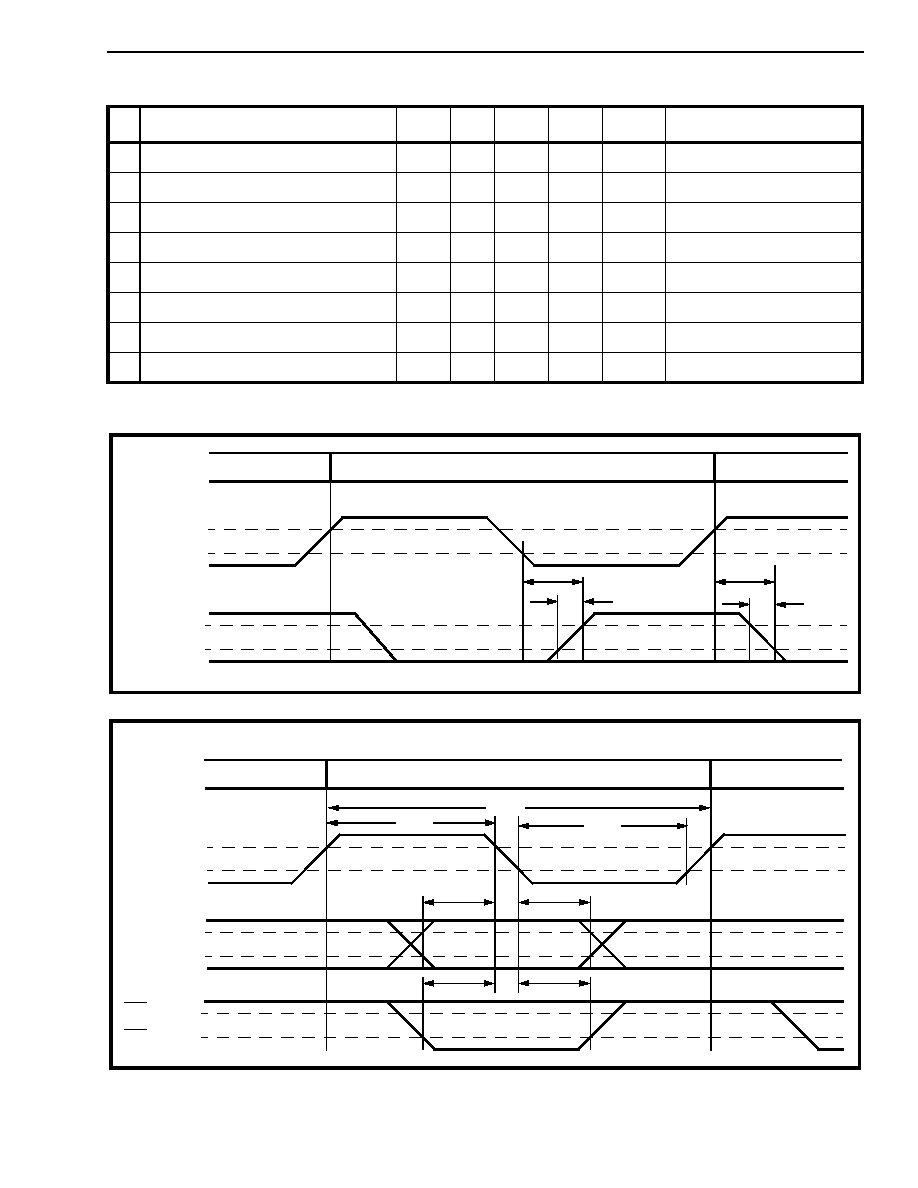
ISO-CMOS
MT8979
4-183
Characteristics are for clocked operation over the ranges of recommended operating temperature and supply voltage.
Typical figures are at 25∞C and are for design aid only: not guaranteed and not subject to production testing.
* The difference between t
TSD
for TxA and TxB is not greater than 20 ns.
Figure 25 - Transmit Timing for CEPT Link
Figure 26 - Receive Timing for CEPT Link
AC Electrical Characteristics
-
CEPT Link Timing (Figures 25 and 26)
Characteristics
Sym
Min
Typ
Max
Units
Test Conditions
1
Transmit Steering Delay*
t
TSD
25
150
ns
200 pF load
2
Transmit Steering Transition Time
t
TST
40
ns
200 pF load
3
E2i Clock Period
t
PEC
400
488
600
ns
4
E2i Clock Width High or Low
t
WEC
200
244
ns
5
Receive Data Setup Time
t
RDS
30
ns
6
Receive Data Hold Time
t
RDH
40
ns
7
Receive Steering Setup Time
t
RSS
30
ns
8
Receive Steering Hold Time
t
RSH
40
ns
Transmitted CEPT Link
Bit Cells
C2i
TxA
or
TxB
V
IH
V
IL
V
OH
V
OL
t
TST
t
TSD
t
TST
t
TSD
Bit Cell
Bit Cells
Received CEPT Link
Bit Cells
E2i
RxA
or
RxB
V
IH
V
IL
V
IH
V
IL
V
IH
V
IL
t
WEC
t
WEC
t
RDS
t
RDH
t
RSS
t
RSH
RxD
t
PEC

MT8979
ISO-CMOS
4-184
Appendix
Control and Status Register Summary
Master Control Word 1 (MCW1) - CSTi0, Channel 15
Master Control Word 2 (MCW2) - CSTi0, Channel 31
Master Control Word 3 (MCW3) - CSTi1, Channel 18
Per Channel Cotnrol Word - CSTi0, Channels 0-14 and 16-30
Channel Associated Signalling - CSTi1, Channels N = 1 to 15
Frame Alignment Signals - CSTi1, Channel 16
Multiframe Alignment Signals - CSTi1, Channel 0
Non-Frame Alignment Signal - CSTi1, Channel 17
7
6
5
4
3
2
1
0
UNUSED
Keep at 1
LOOP16
1 Enabled
0 Disabled
UNUSED
Keep at 1
NDBD
1 No
Debounce
0 Debounce
NDBC
1 No
Debounce
0 Debounce
NDBB
1 No
Debounce
0 Debounce
NDBA
1 No
Debounce
0 Debounce
UNUSED
Keep at 1
UNUSED
Keep at 0
CCS
1 Common
Channel
0 Channel
Associated
8 kHz SEL
1 Enabled
0 Disabled
TXAIS
1 Alarm On
0 Alarm Off
TXTS16AIS
1 Alarm On
0 Alarm Off
XCTL
1 Set High
0 Cleared
UNUSED
UNUSED
Keep at 0
SiMUX
1 Enabled
0 Disabled
RMLOOP
1 Enabled
0 Disabled
HDB3en
1 Disabled
0 Enabled
Maint
1 Enabled
0 Disabled
CRCen
1 Enabled
0 Disabled
DGLOOP
1 Enabled
0 Disabled
ReFR
Device
reframes on
High to Low
Transition
DATA
1 No ADI
0 Enable ADI
LOOP
1 Enabled
0 Disabled
RxPAD4
RxPAD2
RxPAD1
TxPAD4
TxPAD2
TxPAD1
A(N)
Tx
Signalling Bit
B(N)
Tx
Signalling Bit
C(N)
Tx
Signalling Bit
D(N)
Tx
Signalling Bit
A(N + 15)
Tx
Signalling Bit
B(N + 15)
Tx
Signalling Bit
C(N + 15)
Tx
Signalling Bit
D(N + 15)
Tx
Signalling Bit
IUO
Should be
kept at 1
FAF2-8
Frame Alignment Signal - Keep at "0011011"
MA1-4
Multiframe Alignment Signal - Keep at "0000"
X1
Spare Bit
Should be 1
Y
1 Alarm On
0 Alarm Off
X2, X3
Spare Bits - Should be 1
IU1
Reserved for
International
Use
NFAF
Keep at "1"
ALM
1 Alarm On
0 Alarm Off
NU1-5
Bits Reserved for National Use - Should be kept at "1"

ISO-CMOS
MT8979
4-185
Master Control Word 1 (MSW1) - CSTo, Channel 18
Master Status Word 2 (MSW2) - CSTo, Channel 21
Phase Status Word - CSTo, Channel 19
CRC Error Counter - CSTo, Channel 20
Received Channel Associated Signalling - CSTo, Channels N = 1 to 15
Received Frame Alignment Signals - CSTo, Channel 16
Received Multiframe Alignment Signals - CSTo, Channel 0
Received Non-Frame Alignment Signal - CSTo, Channel 17
7
6
5
4
3
2
1
0
TFSYN
1 Out of Sync
0 In Sync
MFSYN
1 Out of Sync
0 In Sync
ERR
Frame
Alignment
Signal Error
Count
SLIP
Changes
State when
Slip
Performed
RXAIS
1 Alarm
Detected
0 No Alarm
TXTS16AIS
1 Alarm
Detected
0 No Alarm
XS
1 XSt High
0 XSt Low
UNUSED
Si2
Remote SMF2
is:
1 Correct
0 Errored
Si1
Remote SMF1
is:
1 Correct
0 Errored
UNUSED
CRC Timer
Transition
from 1 to 0
indicates start
of CRC Error
Counter
CRC Ref
1 Reframed
forced by lack
of CRC frame
CRC Sync
1 CRC Frame
not Detected
0 CRC Frame
Detected
FrmPhase
Bit 8 of Phase
Status Word
TxTSC
Transmit Timeslot Count, Timeslots between F0i and E8Ko
TxBTC
Transmit Bit Count - bit positions within TxTSC
between F0i and E8Ko
CERC 0 - 7
Bits 0 - 7 of CRC Error Counter
A(N)
Rx
Signalling Bit
B(N)
Rx
Signalling Bit
C(N)
Rx
Signalling Bit
D(N)
Rx
Signalling Bit
A(N + 15)
Rx
Signalling Bit
B(N + 15)
Rx
Signalling Bit
C(N + 15)
Rx
Signalling Bit
D(N + 15)
Rx
Signalling Bit
IUO
International
Bit
FAF2-8
Received Frame Alignment Signal
MA1-4
Received Multiframe Alignment Signal
X1
International
Bit
Y
1 Remote MF
Lost
0 Remote MF
Detected
X2, X3
International Bits
IU1
Reserved for
International
Use
NFAF
ALM
1 Detected
0 Not
Detected
NU1-5
Received Bits Reserved for National Use

MT8979
ISO-CMOS
4-186
NOTES: