 | –≠–ª–µ–∫—Ç—Ä–æ–Ω–Ω—ã–π –∫–æ–º–ø–æ–Ω–µ–Ω—Ç: E80271 | –°–∫–∞—á–∞—Ç—å:  PDF PDF  ZIP ZIP |
Jan. 2000
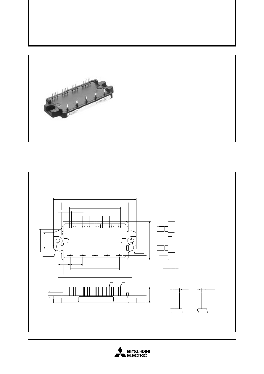
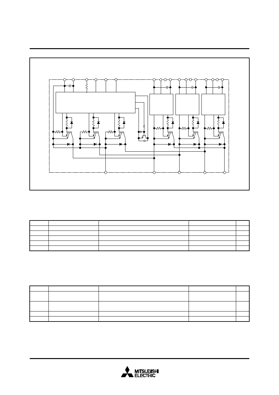
MITSUBISHI <INTELLIGENT POWER MODULES>
PM15CNJ060
FLAT-BASE TYPE
INSULATED PACKAGE
MITSUBISHI <INTELLIGENT POWER MODULES>
PM15CNJ060
FLAT-BASE TYPE
INSULATED PACKAGE
PM15CNJ060
∑
3 phase IGBT (15A/600V) inverter output
∑
Monolithic gate drive & protection logic circuit
∑
Protection logic
∑
Over circuit (OC)
∑
Short circuit (SC)
∑
Over temperature (OT)
∑
Under voltage lock-out (UV)
∑
UL Recognized
File No. E80271
Yellow Card No. E80276
APPLICATION
General purpose inverter, servo drives and other motor controlers
PACKAGE OUTLINES
Dimensions in mm
5.5
5.5
10.5
5.5
3.5
(14.25)
(t = 0.5)
(t = 0.4)
(13.04)
7.62
7.62
7.62
76
19
25.7
2.5
0.5
1.5
0.5
2-R5
2-
4.5
LABEL
B
A
23
22
21
20
19
18
17
16
15
14
13
3
2
1
P
N
U
V
W
4
7
6
5
8
11
10
9
12
94.5
±
1
3.5
±
0.5
33.6
±
0.8
44
±
1
2.54
!
23=58.42
±
0.5
2.54
±
0.25
14
±
0.25
8
±
0.5
18
±
1
84.5
±
0.5
2
±
0.1
0.6
±
0.1
56
±
0.5
71
A:Detail
B:Detail
Terminal code
NC : No Connect
1. V
UPC
2. NC
3. U
P
4. V
UP1
5. V
VPC
6. NC
7. V
P
8. V
VP1
9. V
WPC
10. NC
11. W
P
12. V
WP1
13. V
NC
14. V
N1
15. U
N
16. V
N
17. W
N
18. FO
19. P
20. N
21. U
22. V
23. W
Jan. 2000
MITSUBISHI <INTELLIGENT POWER MODULES>
PM15CNJ060
FLAT-BASE TYPE
INSULATED PACKAGE
INTERNAL FUNCTIONS BLOCK DIAGRAM
V
CES
±
I
C
±
I
CP
P
C
T
j
Collector-Emitter Voltage
Collector Current
Collector Current (Peak)
Collector Dissipation
Junction Temperature
V
D
= 15V, V
CIN
= 15V
T
C
= 25
∞
C
T
C
= 25
∞
C
T
C
= 25
∞
C
V
A
A
W
∞
C
MAXIMUM RATINGS (Tj = 25
∞
C, unless otherwise noted)
INVERTER PART
Symbol
Parameter
Condition
Ratings
Unit
600
15
30
43
≠20 ~ +125
The item defines the maximum junction temperature for the power elements (IGBT/Diode) of the IPM to ensure safe operation. However,
these power elements can endure junction temperature as high as 150
∞
C instantaneously. To make use of this additional temperature al-
lowance, a detailed study of the exact application conditions is required and, accordingly, necessary information is requested to be provided
before use.
V
D
V
CIN
V
FO
I
FO
V
V
V
mA
CONTROL PART
Supply Voltage
Input Voltage
Fault Output Supply Voltage
Fault Output Current
Applied between : V
UP1
-V
UPC
V
VP1
-V
VPC
, V
WP1
-V
WPC
, V
N1
-V
NC
Applied between : U
P
-V
UPC
, V
P
-V
VPC
W
P
-V
WPC
, U
N
∑ V
N
∑ W
N
-V
NC
Applied between : F
O
-V
NC
Sink current at F
O
terminals
20
20
20
20
Symbol
Parameter
Condition
Ratings
Unit
W
P
NC
NC
NC
V
WP1
V
WPC
UN
VN
VN1
VNC
WN
Fo
N
W
V
P
U
V
P
V
VP1
V
VPC
U
P
V
UP1
V
UPC
OUT
Si
GND
Vcc
In
GND
OUT
Si
GND
Vcc
In
GND
O
UN
S
UN
O
WN
S
WN
O
VN
S
VN
Rfo
Fo
GND
Vcc
W
N
V
N
U
N
Rfo=1.5k
Tc
Tb
GND
OUT
Si
GND
Vcc
In
GND

Jan. 2000
MITSUBISHI <INTELLIGENT POWER MODULES>
PM15CNJ060
FLAT-BASE TYPE
INSULATED PACKAGE
TOTAL SYSTEM
Min.
--
--
--
0.3
--
--
--
--
--
--
V
D
= 15V, I
C
= 15A
V
CIN
= 0V, Pulsed
(Fig. 1)
≠I
C
= 15A, V
D
= 15V, V
CIN
= 15V
(Fig. 2)
V
D
= 15V, V
CIN
= 0V
15V
V
CC
= 300V, I
C
= 15A
T
j
= 125
∞
C, Inductive Load
(Upper-Lower Arm)
(Fig. 3)
V
CE
= V
CES
, V
D
= 15V
(Fig. 4)
V
V
µ
s
µ
s
µ
s
µ
s
µ
s
mA
Typ.
1.8
1.9
2.0
0.7
0.15
0.35
1.5
0.4
--
--
Max.
2.5
2.6
3.0
1.6
0.5
1.0
2.3
1.2
1
10
Collector-Emitter
Saturation Voltage
FWDi Forward Voltage
Switching Time
Collector-Emitter
Cutoff Current
ELECTRICAL CHARACTERISTICS (Tj = 25
∞
C, unless otherwise noted)
INVERTER PART
Symbol
Parameter
Test Condition
Unit
Limits
V
CE(sat)
V
EC
t
on
t
rr
t
c(on)
t
off
t
c(off)
I
CES
(Note-1) Tc measurement point
V
CC(PROT)
V
CC(surge)
T
C
T
stg
V
iso
V
V
∞
C
∞
C
V
rms
Supply Voltage Protected
by SC
Supply Voltage
Module Case Operating
Temperature
Storage Temperature
Isolation Voltage
V
D
= 13.5 ~ 16.5V, Inverter Part,
T
j
= 125
∞
C Start
Applied between : P-N, Surge value
(Note-1)
60Hz, Sinusoidal
Charged part to Base, AC 1 min.
Symbol
Parameter
Condition
Ratings
Unit
400
500
≠20 ~ +100
≠40 ~ +125
2500
T
j
= 25
∞
C
T
j
= 125
∞
C
T
j
= 25
∞
C
T
j
= 125
∞
C
Tc

Jan. 2000
MITSUBISHI <INTELLIGENT POWER MODULES>
PM15CNJ060
FLAT-BASE TYPE
INSULATED PACKAGE
(Note-3) With ripple satisfying the following conditions
dv/dt swing
±
5V/
µ
s, Variation
2V peak to peak
V
CC
V
D
V
CIN(ON)
V
CIN(OFF)
f
PWM
t
dead
Applied across P-N terminals
(Fig. 3)
Applied between : V
UP1
-V
UPC
, V
VP1
-V
VPC
V
WP1
-V
WPC
, V
N1
-V
NC
(Note-3)
Applied between : U
P
-V
UPC
, V
P
-V
VPC
, W
P
-V
WPC
U
N
∑ V
N
∑ W
N
-V
NC
Using Application Circuit of Fig. 8
For IPM's each input signals
(Fig. 7)
V
V
V
kHz
µ
s
Supply Voltage
Control Supply Voltage
Input ON Voltage
Input OFF Voltage
PWM Input Frequency
Arm Shoot-through
Blocking Time
RECOMMENDED CONDITIONS FOR USE
Symbol
Parameter
Test Condition
Unit
Recommended value
400
15
±
1.5
0.8
4.0
15
2
--
--
Min.
0.98
10
--
Mounting part
screw : M4
--
N ∑ m
kg ∑ cm
g
Typ.
1.18
12
60
Max.
1.47
15
--
Mounting torque
Weight
MECHANICAL RATINGS AND CHARACTERISTICS
Symbol
Parameter
Test Condition
Unit
Limits
R
th(j-c)Q
R
th(j-c)F
R
th(c-f)
Min.
--
--
--
Inverter IGBT part (per 1/6 module)
Inverter FWDi part (per 1/6 module)
Case to fin, (per 1 module)
Thermal grease applied
∞
C/W
∞
C/W
∞
C/W
Typ.
--
--
--
Max.
2.9
4.5
0.5
Junction to case Thermal
Resistances
Contact Thermal Resistance
THERMAL RESISTANCES
Symbol
Parameter
Test Condition
Unit
Limits
I
D
V
th(ON)
V
th(OFF)
OC
SC
t
off(OC)
OT
OT
r
UV
UV
r
I
FO(H)
I
FO(L)
t
FO
(Note-2) Fault output is given only when the internal SC, OT & UV protections schemes of either upper or lower arm device operate to
protect it.
Min.
--
--
1.2
1.7
18
--
--
100
--
11.5
--
--
--
1.0
V
D
= 15V, V
CIN
= 15V
Applied between : U
P
-V
UPC
, V
P
-V
VPC
, W
P
-V
WPC
U
N
∑ V
N
∑ W
N
-V
NC
≠20
T
j
125
∞
C, V
D
= 15V
(Fig. 5,6)
≠20
T
j
125
∞
C, V
D
= 15V
(Fig. 5,6)
V
D
= 15V
(Fig. 5,6)
V
D
= 15V
≠20
T
j
125
∞
C
V
D
= 15V, V
CIN
= 15V
(Note-2)
V
D
= 15V
(Note-2)
mA
V
V
A
A
µ
s
∞
C
∞
C
V
V
mA
mA
ms
Typ.
18
7
1.5
2.0
26
39
10
110
90
12.0
12.5
--
10
1.8
Max.
25
10
1.8
2.3
--
--
--
120
--
12.5
--
0.01
15
--
Circuit Current
Input ON Voltage
Input OFF Voltage
Over Current Trip Level
Short Circuit Trip Level
Over Current Delay Time
Over Temperature protection
Supply Circuit Under-Voltage
Protection
Fault Output Current
Minimum Fault Output Pulse
Width
CONTROL PART
Trip level
Reset level
Trip level
Reset level
Symbol
Parameter
Test Condition
Unit
Limits
V
N1
-V
NC
V
XP1
-V
XPC

Jan. 2000
MITSUBISHI <INTELLIGENT POWER MODULES>
PM15CNJ060
FLAT-BASE TYPE
INSULATED PACKAGE
PRECAUTIONS FOR TESTING
1. Before appling any control supply voltage (V
D
), the input signals should be low level.
After this, each input signal should be set to the specified ON and OFF level.
2. When performing "SC" tests, the turn-off surge voltage spike at the corresponding protection operation should not be
allowed to rise above V
CC(surge)
rating of the device.
(These test should not be done by using a curve tracer or its equivalent.)
10%
90%
trr
Irr
tr
td (on)
tc (on)
tc (off)
td (off)
V
CIN
Ic
Vce
10%
90%
tf
ton= td (on) + tr
toff= td (off) + tf
V
D (all)
U,V,W, (N)
Signal Input
P, (U,V,W)
A
Pulse
V
CE
V
CIN
(15V)
V
D (all)
U,V,W, (N)
Signal Input
P, (U,V,W)
V
CIN
V
CC
I
C
I
C
I
C
OC
SC
V
CIN
t
off (OC)
t
off (OC)
Short Over Current (sc)
Over Current (oc)
Constant Current
Constant Current
U,V,W
N
V
CINN
V
CINP
V
D
V
D
P
Ic
Vcc
V
CINN
0V
0V
V
CINP
t
t
t
dead
t
dead
Fig. 5 OC and SC Test
Fig. 6 OC and SC Test waveform
Fig. 7 Dead time measurement point example
Fig. 3 Switching time Test circuit and waveform
P, (U,V,W)
P, (U,V,W)
U,V,W, (N)
U,V,W, (N)
VD (all)
VD (all)
V
CIN
(0V)
V
CIN
(15V)
≠Ic
Ic
Fig. 1 V
CE(sat)
Test
Fig. 2 V
EC
Test
V
V
a) Lower Arm Switching
P
N
N
U,V,W
Vcc
Vcc
Ic
Ic
V
D
(all)
P
U,V,W
V
D
(all)
V
CIN
V
CIN
Signal input
(Upper Arm)
Signal input
(Lower Arm)
Signal input
(Upper Arm)
Signal input
(Lower Arm)
b) Upper Arm Switching
Fig. 4 I
CES
Test

Jan. 2000
MITSUBISHI <INTELLIGENT POWER MODULES>
PM15CNJ060
FLAT-BASE TYPE
INSULATED PACKAGE
NOTES FOR STABLE AND SAFE OPERATION ;
∑
Design the PCB pattern to minimize wiring length between opto-coupler and IPM's input terminal, and also to minimize the
stray capacity between the input and output wirings of opto-coupler.
∑
Connect low impedance capacitor between the Vcc and GND terminal of each fast switching opto-coupler.
∑
Fast switching opto-couplers : t
PLH
, t
PHL
0.8
µ
s, Use High CMR type.
∑
Slow switching opto-coupler : CTR
>
100%
∑
Use 4 isolated control power supplies (V
D
). Also, care should be taken to minimize the instantaneous voltage charge of the
power supply.
∑
Make inductance of DC bus line as small as possible, and minimize surge voltage using snubber capacitor between P and N
terminal.
∑
Use line noise filter capacitor (ex. 4.7nF) between each input AC line and ground to reject common-mode noise from AC line
and improve noise immunity of the system.
+
+
+
V
D4
+
V
D1
M
+
-
U
V
W
N
P
20
23
22
21
1
3
2
4
19
V
UPC
V
UP1
NC
NC
NC
U
P
OUT
Si
GND
GND
In
Vcc
V
VPC
V
VP1
V
P
V
WPC
V
WP1
Tc
Tb
GND
VNC
VN1
Fo
WN
VN
UN
W
P
GND
Fo
WN
VN
UN
SVN
OVN
SUN
OUN
SWN
OWN
OUT
Si
GND
GND
In
Vcc
Vcc
Vcc
OUT
Si
GND
GND
In
+
V
D2
+
V
D3
5
7
6
8
9
11
10
12
Fig. 8 Application Example Circuit