 | –≠–ª–µ–∫—Ç—Ä–æ–Ω–Ω—ã–π –∫–æ–º–ø–æ–Ω–µ–Ω—Ç: M16C62A | –°–∫–∞—á–∞—Ç—å:  PDF PDF  ZIP ZIP |

Mitsubishi microcomputers
M16C / 62A Group
SINGLE-CHIP 16-BIT CMOS MICROCOMPUTER
Description
1
------Table of Contents------
Description
The M16C/62A group of single-chip microcomputers are built using the high-performance silicon gate
CMOS process using a M16C/60 Series CPU core and are packaged in a 100-pin plastic molded QFP.
These single-chip microcomputers operate using sophisticated instructions featuring a high level of instruc-
tion efficiency. With 1M bytes of address space, they are capable of executing instructions at high speed.
They also feature a built-in multiplier and DMAC, making them ideal for controlling office, communications,
industrial equipment, and other high-speed processing applications.
The M16C/62A group includes a wide range of products with different internal memory types and sizes and
various package types.
Features
∑ Memory capacity .................................. ROM (See Figure 1.1.4. ROM Expansion)
RAM 3K to 20K bytes
∑ Shortest instruction execution time ...... 62.5ns (f(X
IN
)=16MH
Z
, V
CC
=5V)
100ns (f(X
IN
)=10MH
Z
, V
CC
=3V, with software one-wait) : Mask ROM, flash memory 5V version
∑ Supply voltage ..................................... 4.2V to 5.5V (f(X
IN
)=16MH
Z
, without software wait) : Mask ROM, flash memory 5V version
2.7V to 5.5V (f(X
IN
)=10MH
Z
with software one-wait) : Mask ROM, flash memory 5V version
∑ Low power consumption ...................... 25.5mW ( f(X
IN
)=10MH
Z
, with software one-wait, V
CC
= 3V)
∑ Interrupts .............................................. 25 internal and 8 external interrupt sources, 4 software
interrupt sources; 7 levels (including key input interrupt)
∑ Multifunction 16-bit timer ...................... 5 output timers + 6 input timers
∑ Serial I/O .............................................. 5 channels (3 for UART or clock synchronous, 2 for clock synchro-
nous)
∑ DMAC .................................................. 2 channels (trigger: 24 sources)
∑ A-D converter ....................................... 10 bits X 8 channels (Expandable up to 10 channels)
∑ D-A converter ....................................... 8 bits X 2 channels
∑ CRC calculation circuit ......................... 1 circuit
∑ Watchdog timer .................................... 1 line
∑ Programmable I/O ............................... 87 lines
∑ Input port ..............................................
_______
1 line (P8
5
shared with NMI pin)
∑ Memory expansion .............................. Available (to a maximum of 1M bytes)
∑ Chip select output ................................ 4 lines
∑ Clock generating circuit ....................... 2 built-in clock generation circuits
(built-in feedback resistor, and external ceramic or quartz oscillator)
Applications
Audio, cameras, office equipment, communications equipment, portable equipment
Timer ............................................................. 77
Serial I/O ..................................................... 107
A-D Converter ............................................. 148
D-A Converter ............................................. 158
CRC Calculation Circuit .............................. 160
Programmable I/O Ports ............................. 162
Electrical characteristic ............................... 173
Flash memory version ................................. 216
Central Processing Unit (CPU) ..................... 11
Reset ............................................................. 14
Processor Mode ............................................ 21
Clock Generating Circuit ............................... 35
Protection ...................................................... 44
Interrupts ....................................................... 45
Watchdog Timer ............................................ 65
DMAC ........................................................... 67

Mitsubishi microcomputers
M16C / 62A Group
SINGLE-CHIP 16-BIT CMOS MICROCOMPUTER
Description
2
1
2
3
4
5
6
7
8
9 10 11 12 13 14 15 16 17 18 19 20 21 22 23 24 25 26 27 28 29 30
31
32
33
34
35
36
37
38
39
40
41
42
43
44
45
46
47
48
49
50
51
52
53
54
55
56
57
58
59
60
61
62
63
64
65
66
67
68
69
70
71
72
73
74
75
76
77
78
79
80
81
82
83
84
85
86
87
88
89
90
91
92
93
94
95
96
97
98
99
100
P0
0
/D
0
P0
1
/D
1
P0
2
/D
2
P0
3
/D
3
P0
4
/D
4
P0
5
/D
5
P0
6
/D
6
P0
7
/D
7
P1
0
/D
8
P1
1
/D
9
P1
2
/D
10
P1
3
/D
11
P1
4
/D
12
V
REF
AV
SS
V
CC
X
IN
X
OUT
V
SS
RESET
CNVss
P8
7
/X
CIN
P8
6
/X
COUT
BYTE
P2
0
/A
0
(/D
0
/-)
P2
1
/A
1
(/D
1
/D
0
)
P2
2
/A
2
(/D
2
/D
1
)
P2
3
/A
3
(/D
3
/D
2
)
P2
4
/A
4
(/D
4
/D
3
)
P2
5
/A
5
(/D
5
/D
4
)
P2
6
/A
6
(/D
6
/D
5
)
P2
7
/A
7
(/D
7
/D
6
)
P3
0
/A
8
(/-/D
7
)
P3
1
/A
9
P3
2
/A
10
P3
3
/A
11
P3
4
/A
12
P3
5
/A
13
P3
6
/A
14
P3
7
/A
15
P4
0
/A
16
P4
1
/A
17
P4
2
/A
18
P4
3
/A
19
P7
4
/TA2
OUT
/W
P7
6
/TA3
OUT
P5
6
/ALE
P7
7
/TA3
IN
P5
5
/HOLD
P5
4
/HLDA
P5
3
/BCLK
P5
2
/RD
Vcc
Vss
P5
7
/RDY/CLK
OUT
P4
5
/CS1
P4
6
/CS2
P4
7
/CS3
AVcc
P6
3
/T
X
D
0
P6
5
/CLK
1
P6
6
/RxD
1
P6
7
/T
X
D
1
P6
1
/CLK
0
P6
2
/RxD
0
P10
0
/AN
0
P10
1
/AN
1
P10
2
/AN
2
P10
3
/AN
3
P9
3
/DA
0
/TB3
IN
P9
4
/DA
1
/TB4
IN
P9
5
/ANEX0/CLK4
P9
6
/ANEX1/S
OUT
4
P9
1
/TB1
IN
/S
IN
3
P9
2
/TB2
IN
/S
OUT
3
P8
0
/TA4
OUT
/U
P6
0
/CTS
0
/RTS
0
P6
4
/CTS
1
/RTS
1
/CLKS
1
P7
2
/CLK
2
/TA1
OUT
/V
P8
2
/INT
0
P7
1
/RxD
2
/SCL/TA0
IN
/TB5
IN
(Note)
P8
3
/INT
1
P8
5
/NMI
P9
7
/AD
TRG
/S
IN
4
P4
4
/CS0
P5
0
/WRL/WR
P5
1
/WRH/BHE
P9
0
/TB0
IN
/CLK3
P7
0
/T
X
D
2
/SDA/TA0
OUT
(Note)
P8
4
/INT
2
P8
1
/TA4
IN
/U
P7
5
/TA2
IN
/W
P1
5
/D
13
/INT3
P1
6
/D
14
/INT4
P1
7
/D
15
/INT5
P10
7
/AN
7
/KI
3
P10
6
/AN
6
/KI
2
P10
5
/AN
5
/KI
1
P10
4
/AN
4/
KI
0
P7
3
/CTS
2
/RTS
2
/TA1
IN
/V
Note: P7
0
and P7
1
are N channel open-drain output pin.
Pin Configuration
Figures 1.1.1 and 1.1.2 show the pin configurations (top view).
PIN CONFIGURATION (top view)
Package: 100P6S-A
Figure 1.1.1. Pin configuration (top view)
M16C/62A Group

Mitsubishi microcomputers
M16C / 62A Group
SINGLE-CHIP 16-BIT CMOS MICROCOMPUTER
Description
3
1 2
3
4
5
6
7
8 9 10 11 12 13 14 15 16 17 18 19 20 21 22 23 24 25
26
27
28
29
30
31
32
33
34
35
36
37
38
39
40
41
42
43
44
45
46
47
48
49
50
51
52
53
54
55
56
57
58
59
60
61
62
63
64
65
66
67
68
69
70
71
72
73
74
75
76
77
78
79
80
81
82
83
84
85
86
87
88
89
90
91
92
93
94
95
96
97
98
99
100
P0
0
/D
0
P0
1
/D
1
P0
2
/D
2
P0
3
/D
3
P0
4
/D
4
P0
5
/D
5
P0
6
/D
6
P0
7
/D
7
P1
0
/D
8
P1
1
/D
9
P1
2
/D
10
P1
3
/D
11
P1
4
/D
12
V
REF
AV
SS
V
CC
X
IN
X
OUT
V
SS
RESET
CNVss
P8
7
/X
CIN
P8
6
/X
COUT
BYTE
P2
0
/A
0
(/D
0
/-)
P2
1
/A
1
(/D
1
/D
0
)
P2
2
/A
2
(/D
2
/D
1
)
P2
3
/A
3
(/D
3
/D
2
)
P2
4
/A
4
(/D
4
/D
3
)
P2
5
/A
5
(/D
5
/D
4
)
P2
6
/A
6
(/D
6
/D
5
)
P2
7
/A
7
(/D
7
/D
6
)
P3
0
/A
8
(/-/D
7
)
P3
1
/A
9
P3
2
/A
10
P3
3
/A
11
P3
4
/A
12
P3
5
/A
13
P3
6
/A
14
P3
7
/A
15
P4
0
/A
16
P4
1
/A
17
P4
2
/A
18
P4
3
/A
19
P7
4
/TA2
OUT
/W
P7
6
/TA3
OUT
P5
6
/ALE
P7
7
/TA3
IN
P5
5
/HOLD
P5
4
/HLDA
P5
3
/BCLK
P5
2
/RD
Vcc
Vss
P5
7
/RDY/CLK
OUT
P4
5
/CS1
P4
6
/CS2
P4
7
/CS3
AVcc
P6
3
/T
X
D
0
P6
5
/CLK
1
P6
6
/RxD
1
P6
7
/T
X
D
1
P6
1
/CLK
0
P6
2
/RxD
0
P10
0
/AN
0
P10
1
/AN
1
P10
2
/AN
2
P10
3
/AN
3
P9
3
/DA
0
/TB3
IN
P9
4
/DA
1
/TB4
IN
P9
5
/ANEX0/CLK4
P9
6
/ANEX1/S
OUT
4
P9
1
/TB1
IN
/S
IN
3
P9
2
/TB2
IN
/S
OUT
3
P8
1
/TA4
IN
/U
P8
0
/TA4
OUT
/U
P6
0
/CTS
0
/RTS
0
P6
4
/CTS
1
/RTS
1
/CLKS
1
P8
2
/INT
0
P8
3
/INT
1
P8
5
/NMI
P9
7
/AD
TRG
/S
IN
4
P4
4
/CS0
P5
0
/WRL/WR
P5
1
/WRH/BHE
P9
0
/TB0
IN
/CLK3
P8
4
/INT
2
P7
2
/CLK
2
/TA1
OUT
/V
P7
1
/RxD
2
/SCL/TA0
IN
/TB5
IN
(Note)
P7
0
/T
X
D
2
/SDA/TA0
OUT
(Note)
P7
5
/TA2
IN
/W
P7
3
/CTS
2
/RTS
2
/TA1
IN
/V
P1
5
/D
13
/INT
3
P1
6
/D
14
/INT
4
P1
7
/D
15
/INT
5
P10
7
/AN
7
/KI
3
P10
6
/AN
6
/KI
2
P10
5
/AN
5
/KI
1
P10
4
/AN
4/
KI
0
Note: P7
0
and P7
1
are N channel open-drain output pin.
Figure 1.1.2. Pin configuration (top view)
Package: 100P6Q-A
PIN CONFIGURATION (top view)
M16C/62A Group

Mitsubishi microcomputers
M16C / 62A Group
SINGLE-CHIP 16-BIT CMOS MICROCOMPUTER
Description
4
Block Diagram
Figure 1.1.3 is a block diagram of the M16C/62A group.
Timer
Timer TA0 (16 bits)
Timer TA1 (16 bits)
Timer TA2 (16 bits)
Timer TA3 (16 bits)
Timer TA4 (16 bits)
Timer TB0 (16 bits)
Timer TB1 (16 bits)
Timer TB2 (16 bits)
Timer TB3 (16 bits)
Timer TB4 (16 bits)
Timer TB5 (16 bits)
Internal peripheral functions
Watchdog timer
(15 bits)
DMAC
(2 channels)
D-A converter
(8 bits X 2 channels)
A-D converter
(10 bits
X
8 channels
Expandable up to 10 channels)
UART/clock synchronous SI/O
(8 bits
X
3 channels)
System clock generator
X
IN
-X
OUT
X
CIN
-X
COUT
M16C/60 series16-bit CPU core
I/O ports
Port P0
8
Port P1
8
Port P2
8
Port P3
8
Port P4
8
Port P5
8
Port P6
8
8
R0L
R0H
R1H
R1L
R2
R3
A0
A1
FB
R0L
R0H
R1H
R1L
R2
R3
A0
A1
FB
Registers
ISP
USP
Stack pointer
CRC arithmetic circuit (CCITT )
(Polynomial : X
16
+X
12
+X
5
+1)
Multiplier
7
8
8
Port P10
Port P9
Port P8
Port P7
Memory
Port P8
5
ROM
(Note 1)
RAM
(Note 2)
Note 1: ROM size depends on MCU type.
Note 2: RAM size depends on MCU type.
SB
FLG
PC
Program counter
Clock synchronous SI/O
(8 bits
X
2 channels)
Vector table
INTB
Flag register
Figure 1.1.3. Block diagram of M16C/62A group
Mitsubishi microcomputers
M16C / 62A Group
SINGLE-CHIP 16-BIT CMOS MICROCOMPUTER
Description
5
Item
Performance
Number of basic instructions
91 instructions
Shortest instruction execution time
62.5ns(f(X
IN
)=16MH
Z
, V
CC
=5V)
100ns (f(X
IN
)=10MH
Z
, V
CC
=3V, with software one-wait)
: Mask ROM, flash memory 5V version
Memory
ROM
(See the figure 1.1.4. ROM Expansion)
capacity
RAM
3K to 20K bytes
I/O port
P0 to P10 (except P8
5
)
8 bits x 10, 7 bits x 1
Input port
P8
5
1 bit x 1
Multifunction TA0, TA1, TA2, TA3, TA4
16 bits x 5
timer
TB0, TB1, TB2, TB3, TB4, TB5
16 bits x 6
Serial I/O
UART0, UART1, UART2
(UART or clock synchronous) x 3
SI/O3, SI/O4
(Clock synchronous) x 2
A-D converter
10 bits x (8 + 2) channels
D-A converter
8 bits x 2
DMAC
2 channels (trigger: 24 sources)
CRC calculation circuit
CRC-CCITT
Watchdog timer
15 bits x 1 (with prescaler)
Interrupt
25 internal and 8 external sources, 4 software sources, 7 levels
Clock generating circuit
2 built-in clock generation circuits
(built-in feedback resistor, and external ceramic or quartz oscillator)
Supply voltage
4.2V to 5.5V (f(X
IN
)=16MH
Z
, without software wait)
: Mask ROM, flash memory 5V version
2.7V to 5.5V (f(X
IN
)=10MH
Z
with software one-wait)
: Mask ROM, flash memory 5V version
Power consumption
25.5mW (f(X
IN
) = 10MH
Z
, V
CC
=3V with software one-wait)
I/O
I/O withstand voltage
5V
characteristics Output current
5mA
Memory expansion
Available (to a maximum of 1M bytes)
Device configuration
CMOS high performance silicon gate
Package
100-pin plastic mold QFP
Table 1.1.1. Performance outline of M16C/62A group
Performance Outline
Table 1.1.1 is a performance outline of M16C/62A group.

Mitsubishi microcomputers
M16C / 62A Group
SINGLE-CHIP 16-BIT CMOS MICROCOMPUTER
Description
6
Mitsubishi plans to release the following products in the M16C/62A group:
(1) Support for mask ROM version, external ROM version, and flash memory version
(2) ROM capacity
(3) Package
100P6S-A
: Plastic molded QFP (mask ROM, and flash memory versions)
100P6Q-A
: Plastic molded QFP(mask ROM, and flash memory versions)
The M16C/62A group products currently supported are listed in Table 1.1.2.
Table 1.1.2. M16C/62A group
ROM Size
(Byte)
External
ROM
128K
96K
64K
32K
M30620M8A-XXXFP/GP
M30622M8A-XXXFP/GP
M30620MAA-XXXFP/GP
M30622MAA-XXXFP/GP
M30620MCA-XXXFP/GP
M30622MCA-XXXFP/GP
Mask ROM version
Flash memory version
M30624FGAFP/GP
256K
M30624MGA-XXXFP/GP
M30622M4A-XXXFP/GP
External ROM version
M30620SAFP/GP
M30622SAFP/GP
M30620FCAFP/GP
RAM capacity
ROM capacity
Package type
Remarks
Type No.
March. 2001
M30622M4A-XXXFP
3K byte
100P6S-A
M30622M4A-XXXGP
100P6Q-A
M30620M8A-XXXFP
64K byte
10K byte
100P6S-A
Mask ROM version
M30620M8A-XXXGP
100P6Q-A
M30622M8A-XXXFP
4K byte
100P6S-A
M30622M8A-XXXGP
100P6Q-A
M30620MAA-XXXFP
10K byte
100P6S-A
3K byte
M30622SAFP
External ROM
version
M30622SAGP
100P6Q-A
100P6S-A
10K byte
M30620MCA-XXXGP
M30620MCA-XXXFP
M30622MCA-XXXFP
M30622MCA-XXXGP
5K byte
128K byte
100P6S-A
100P6Q-A
100P6S-A
100P6Q-A
100P6S-A
M30620SAFP
10K byte
100P6Q-A
M30620SAGP
M30620MAA-XXXGP
96K byte
100P6Q-A
M30622MAA-XXXFP
5K byte
100P6S-A
M30622MAA-XXXGP
100P6Q-A
M30624MGA-XXXFP
20K byte
100P6S-A
M30624MGA-XXXGP
100P6Q-A
256K byte
M30624FGAFP
M30624FGAGP
20K byte
256K byte
Flash memory
5V version
100P6S-A
100P6Q-A
32K byte
**
: Under development
**
M30620FCAFP
M30620FCAGP
10K byte
128K byte
100P6S-A
100P6Q-A
Figure 1.1.4. ROM expansion

Mitsubishi microcomputers
M16C / 62A Group
SINGLE-CHIP 16-BIT CMOS MICROCOMPUTER
Description
7
Package type:
FP : Package
100P6S-A
GP :
100P6Q-A
ROM No.
Omitted for flash memory version
ROM capacity:
4 : 32K bytes
8 : 64K bytes
A : 96K bytes
C : 128K bytes
G: 256K bytes
Memory type:
M : Mask ROM version
S : External ROM version
F : Flash memory version
Type No. M 3 0 6 2 2 M 8 A≠ X X X F P
M16C/62 Group
M16C Family
Shows RAM capacity, pin count, etc
(The value itself has no specific meaning)
Figure 1.1.5. Type No., memory size, and package

Mitsubishi microcomputers
M16C / 62A Group
SINGLE-CHIP 16-BIT CMOS MICROCOMPUTER
Pin Description
8
V
CC
, V
SS
CNV
SS
X
IN
X
OUT
BYTE
AV
CC
AV
SS
V
REF
P0
0
to P0
7
D
0
to D
7
P1
0
to P1
7
D
8
to D
15
P2
0
to P2
7
A
0
to A
7
A
0
/D
0
to
A
7
/D
7
A
0
A
1
/D
0
to A
7
/D
6
P3
0
to P3
7
A
8
to A
15
A
8
/D
7
,
A
9
to A
15
P4
0
to P4
7
Signal name
Power supply
input
CNV
SS
Reset input
Clock input
Clock output
External data
bus width
select input
Analog power
supply input
Reference
voltage input
I/O port P0
I/O port P1
I/O port P2
I/O port P3
I/O port P4
Supply 2.7V to 5.5 V to the V
CC
pin. Supply 0 V to the V
SS
pin.
Function
This pin switches between processor modes. Connect this pin to the
V
SS
pin when after a reset you want to start operation in single-chip
mode (memory expansion mode) or the V
CC
pin when starting
operation in microprocessor mode.
A "L" on this input resets the microcomputer.
These pins are provided for the main clock generating circuit.Connect
a ceramic resonator or crystal between the X
IN
and the X
OUT
pins. To
use an externally derived clock, input it to the X
IN
pin and leave the
X
OUT
pin open.
This pin selects the width of an external data bus. A 16-bit width is
selected when this input is "L"; an 8-bit width is selected when this
input is "H". This input must be fixed to either "H" or "L". Connect this
pin to the V
SS
pin when not using external data bus.
This pin is a power supply input for the A-D converter. Connect this
pin to V
CC
.
This pin is a power supply input for the A-D converter. Connect this
pin to V
SS
.
This pin is a reference voltage input for the A-D converter.
This is an 8-bit CMOS I/O port. It has an input/output port direction
register that allows the user to set each pin for input or output
individually. When used for input in single-chip mode, the port can be
set to have or not have a pull-up resistor in units of four bits by
software. In memory expansion and microprocessor modes, selection
of the internal pull-resistor is not available.
When set as a separate bus, these pins input and output data (D
0
≠D
7
).
This is an 8-bit I/O port equivalent to P0. P1
5
to P1
7
also function as
external interrupt pins as selected by software.
When set as a separate bus, these pins input and output data
(D
8
≠D
15
).
This is an 8-bit I/O port equivalent to P0.
These pins output 8 low-order address bits (A
0
≠A
7
).
If the external bus is set as an 8-bit wide multiplexed bus, these pins
input and output data (D
0
≠D
7
) and output 8 low-order address bits
(A
0
≠A
7
) separated in time by multiplexing.
If the external bus is set as a 16-bit wide multiplexed bus, these pins
input and output data (D
0
≠D
6
) and output address (A
1
≠A
7
) separated
in time by multiplexing. They also output address (A
0
).
This is an 8-bit I/O port equivalent to P0.
These pins output 8 middle-order address bits (A
8
≠A
15
).
If the external bus is set as a 16-bit wide multiplexed bus, these pins
input and output data (D
7
) and output address (A
8
) separated in time
by multiplexing. They also output address (A
9
≠A
15
).
This is an 8-bit I/O port equivalent to P0.
Pin name
Input
Input
Input
Output
Input
Input
Input/output
Input/output
Input/output
Input/output
I/O type
Analog power
supply input
Input/output
Output
Input/output
Output
Input/output
Input/output
Output
Input/output
Output
Input/output
Output
Output
A
16
to A
19
,
CS
0
to CS
3
These pins output A
16
≠A
19
and CS
0
≠CS
3
signals. A
16
≠A
19
are 4 high-
order address bits. CS
0
≠CS
3
are chip select signals used to specify an
access space.
RESET
Pin Description

Pin Description
Mitsubishi microcomputers
M16C / 62A Group
SINGLE-CHIP 16-BIT CMOS MICROCOMPUTER
9
Pin Description
Signal name
Function
Pin name
I/O type
I/O port P5
Input/output
Input/output
Input/output
Input/output
Input/output
Input/output
Input
Input/output
Input/output
I/O port P6
I/O port P7
I/O port P8
I/O port P8
5
I/O port P9
I/O port P10
P5
0
to P5
7
P6
0
to P6
7
P7
0
to P7
7
P8
0
to P8
4
,
P8
6
,
P8
7
,
P8
5
P9
0
to P9
7
P10
0
to P10
7
This is an 8-bit I/O port equivalent to P0. In single-chip mode, P5
7
in
this port outputs a divide-by-8 or divide-by-32 clock of X
IN
or a clock of
the same frequency as X
CIN
as selected by software.
Output
Output
Output
Output
Output
Input
Output
Input
This is an 8-bit I/O port equivalent to P0. When used for input in single-
chip, memory expansion, and microprocessor modes, the port can be
set to have or not have a pull-up resistor in units of four bits by
software. Pins in this port also function as UART0 and UART1 I/O pins
as selected by software.
This is an 8-bit I/O port equivalent to P6 (P7
0
and P7
1
are N channel
open-drain output). Pins in this port also function as timer A
0
≠A
3
,
timer B5 or UART2 I/O pins as selected by software.
This is an 8-bit I/O port equivalent to P6. Pins in this port also function
as SI/O3, 4 I/O pins, Timer B0≠B4 input pins, D-A converter output pins,
A-D converter extended input pins, or A-D trigger input pins as selected
by software.
This is an 8-bit I/O port equivalent to P6. Pins in this port also function
as A-D converter input pins as selected by software. Furthermore, P10
4
≠P10
7
also function as input pins for the key input interrupt function.
WRL / WR,
WRH / BHE,
RD,
BCLK,
HLDA,
HOLD,
ALE,
RDY
Output WRL, WRH (WR and BHE), RD, BCLK, HLDA, and ALE
signals. WRL and WRH, and BHE and WR can be switched using
software control.
WRL, WRH, and RD selected
With a 16-bit external data bus, data is written to even addresses
when the WRL signal is "L" and to the odd addresses when the WRH
signal is "L". Data is read when RD is "L".
WR, BHE, and RD selected
Data is written when WR is "L". Data is read when RD is "L". Odd
addresses are accessed when BHE is "L". Use this mode when using
an 8-bit external data bus.
While the input level at the HOLD pin is "L", the microcomputer is
placed in the hold state. While in the hold state, HLDA outputs a "L"
level. ALE is used to latch the address. While the input level of the
RDY pin is "L", the microcomputer is in the ready state.
P8
0
to P8
4
, P8
6
, and P8
7
are I/O ports with the same functions as P6.
Using software, they can be made to function as the I/O pins for timer
A4 and the input pins for external interrupts. P8
6
and P8
7
can be set
using software to function as the I/O pins for a sub clock generation
circuit. In this case, connect a quartz oscillator between P8
6
(X
COUT
pin) and P8
7
(X
CIN
pin). P8
5
is an input-only port that also functions
for NMI. The NMI interrupt is generated when the input at this pin
changes from "H" to "L". The NMI function cannot be cancelled using
software. The pull-up cannot be set for this pin.
Mitsubishi microcomputers
M16C / 62A Group
SINGLE-CHIP 16-BIT CMOS MICROCOMPUTER
Memory
10
Operation of Functional Blocks
The M16C/62A group accommodates certain units in a single chip. These units include ROM and RAM to
store instructions and data and the central processing unit (CPU) to execute arithmetic/logic operations.
Also included are peripheral units such as timers, serial I/O, D-A converter, DMAC, CRC calculation circuit,
A-D converter, and I/O ports.
The following explains each unit.
Memory
Figure 1.3.1 is a memory map of the M16C/62A group. The address space extends the 1M bytes from
address 00000
16
to FFFFF
16
. From FFFFF
16
down is ROM. For example, in the M30622MCA-XXXFP,
there is 128K bytes of internal ROM from E0000
16
to FFFFF
16
. The vector table for fixed interrupts such as
_______
the reset and NMI are mapped to FFFDC
16
to FFFFF
16
. The starting address of the interrupt routine is
stored here. The address of the vector table for timer interrupts, etc., can be set as desired using the
internal register (INTB). See the section on interrupts for details.
From 00400
16
up is RAM. For example, in the M30622MCA-XXXFP, 5K bytes of internal RAM is mapped
to the space from 00400
16
to 017FF
16
. In addition to storing data, the RAM also stores the stack used when
calling subroutines and when interrupts are generated.
The SFR area is mapped to 00000
16
to 003FF
16
. This area accommodates the control registers for periph-
eral devices such as I/O ports, A-D converter, serial I/O, and timers, etc. Figures 1.6.1 to 1.6.3 are location
of peripheral unit control registers. Any part of the SFR area that is not occupied is reserved and cannot be
used for other purposes.
The special page vector table is mapped to FFE00
16
to FFFDB
16
. If the starting addresses of subroutines
or the destination addresses of jumps are stored here, subroutine call instructions and jump instructions
can be used as 2-byte instructions, reducing the number of program steps.
In memory expansion mode and microprocessor mode, a part of the spaces are reserved and cannot be
used. For example, in the M30622MCA-XXXFP, the following spaces cannot be used.
∑ The space between 01800
16
and 03FFF
16
(Memory expansion and microprocessor modes)
∑ The space between D0000
16
and DFFFF
16
(Memory expansion mode)
Figure 1.3.1. Memory map
00000
16
YYYYY
16
FFFFF
16
00400
16
04000
16
XXXXX
16
D0000
16
External area
Internal ROM area
SFR area
For details, see Figures
1.6.1 to 1.6.3
Internal RAM area
Internal reserved
area (Note 1)
Internal reserved
area (Note 2)
FFE00
16
FFFDC
16
FFFFF
16
Note 1: During memory expansion and microprocessor modes, can not be used.
Note 2: In memory expansion mode, can not be used.
Note 3: These memory maps show an instance in which PM13 is set to 0; but in the
case of products in which the internal RAM and the internal ROM are expanded
to over 15 Kbytes and 192 Kbytes, respectively, they show an instance in which
PM13 is set to 1.
Undefined instruction
Overflow
BRK instruction
Address match
Single step
Watchdog timer
Reset
Special page
vector table
DBC
NMI
Address YYYYY
16
3K bytes
00FFF
16
053FF
16
017FF
16
013FF
16
Address XXXXX
16
ROM size
02BFF
16
5K bytes
4K bytes
10K bytes
20K bytes
RAM size
32K bytes
C0000
16
E8000
16
F0000
16
E0000
16
96K bytes
64K bytes
128K bytes
256K bytes
F8000
16

Mitsubishi microcomputers
M16C / 62A Group
SINGLE-CHIP 16-BIT CMOS MICROCOMPUTER
CPU
11
Central Processing Unit (CPU)
The CPU has a total of 13 registers shown in Figure 1.4.1. Seven of these registers (R0, R1, R2, R3, A0,
A1, and FB) come in two sets; therefore, these have two register banks.
(1) Data registers (R0, R0H, R0L, R1, R1H, R1L, R2, and R3)
Data registers (R0, R1, R2, and R3) are configured with 16 bits, and are used primarily for transfer and
arithmetic/logic operations.
Registers R0 and R1 each can be used as separate 8-bit data registers, high-order bits as (R0H/R1H),
and low-order bits as (R0L/R1L). In some instructions, registers R2 and R0, as well as R3 and R1 can
use as 32-bit data registers (R2R0/R3R1).
(2) Address registers (A0 and A1)
Address registers (A0 and A1) are configured with 16 bits, and have functions equivalent to those of data
registers. These registers can also be used for address register indirect addressing and address register
relative addressing.
In some instructions, registers A1 and A0 can be combined for use as a 32-bit address register (A1A0).
H
L
b15
b8
b7
b0
R0
(Note)
H
L
b15
b8
b7
b0
R1
(Note)
R2
(Note)
b15
b0
R3
(Note)
b15
b0
A0
(Note)
b15
b0
A1
(Note)
b15
b0
FB
(Note)
b15
b0
Data
registers
Address
registers
Frame base
registers
b15
b0
b15
b0
b15
b0
b15
b0
b0
b19
b0
b19
H
L
Program counter
Interrupt table
register
User stack pointer
Interrupt stack
pointer
Static base
register
Flag register
PC
INTB
USP
ISP
SB
FLG
Note: These registers consist of two register banks.
C
D
Z
S
B
O
I
U
IPL
Figure 1.4.1. Central processing unit register

Mitsubishi microcomputers
M16C / 62A Group
SINGLE-CHIP 16-BIT CMOS MICROCOMPUTER
CPU
12
(3) Frame base register (FB)
Frame base register (FB) is configured with 16 bits, and is used for FB relative addressing.
(4) Program counter (PC)
Program counter (PC) is configured with 20 bits, indicating the address of an instruction to be executed.
(5) Interrupt table register (INTB)
Interrupt table register (INTB) is configured with 20 bits, indicating the start address of an interrupt vector
table.
(6) Stack pointer (USP/ISP)
Stack pointer comes in two types: user stack pointer (USP) and interrupt stack pointer (ISP), each config-
ured with 16 bits.
Your desired type of stack pointer (USP or ISP) can be selected by a stack pointer select flag (U flag).
This flag is located at the position of bit 7 in the flag register (FLG).
(7) Static base register (SB)
Static base register (SB) is configured with 16 bits, and is used for SB relative addressing.
(8) Flag register (FLG)
Flag register (FLG) is configured with 11 bits, each bit is used as a flag. Figure 1.4.2 shows the flag
register (FLG). The following explains the function of each flag:
∑ Bit 0: Carry flag (C flag)
This flag retains a carry, borrow, or shift-out bit that has occurred in the arithmetic/logic unit.
∑ Bit 1: Debug flag (D flag)
This flag enables a single-step interrupt.
When this flag is "1", a single-step interrupt is generated after instruction execution. This flag is
cleared to "0" when the interrupt is acknowledged.
∑ Bit 2: Zero flag (Z flag)
This flag is set to "1" when an arithmetic operation resulted in 0; otherwise, cleared to "0".
∑ Bit 3: Sign flag (S flag)
This flag is set to "1" when an arithmetic operation resulted in a negative value; otherwise, cleared to "0".
∑ Bit 4: Register bank select flag (B flag)
This flag chooses a register bank. Register bank 0 is selected when this flag is "0" ; register bank 1 is
selected when this flag is "1".
∑ Bit 5: Overflow flag (O flag)
This flag is set to "1" when an arithmetic operation resulted in overflow; otherwise, cleared to "0".
∑ Bit 6: Interrupt enable flag (I flag)
This flag enables a maskable interrupt.
An interrupt is disabled when this flag is "0", and is enabled when this flag is "1". This flag is cleared to
"0" when the interrupt is acknowledged.

Mitsubishi microcomputers
M16C / 62A Group
SINGLE-CHIP 16-BIT CMOS MICROCOMPUTER
CPU
13
∑ Bit 7: Stack pointer select flag (U flag)
Interrupt stack pointer (ISP) is selected when this flag is "0" ; user stack pointer (USP) is selected
when this flag is "1".
This flag is cleared to "0" when a hardware interrupt is acknowledged or an INT instruction of software
interrupt Nos. 0 to 31 is executed.
∑ Bits 8 to 11: Reserved area
∑ Bits 12 to 14: Processor interrupt priority level (IPL)
Processor interrupt priority level (IPL) is configured with three bits, for specification of up to eight
processor interrupt priority levels from level 0 to level 7.
If a requested interrupt has priority greater than the processor interrupt priority level (IPL), the interrupt
is enabled.
∑ Bit 15: Reserved area
The C, Z, S, and O flags are changed when instructions are executed. See the software manual for
details.
Figure 1.4.2. Flag register (FLG)
Carry flag
Debug flag
Zero flag
Sign flag
Register bank select flag
Overflow flag
Interrupt enable flag
Stack pointer select flag
Reserved area
Processor interrupt priority level
Reserved area
Flag register (FLG)
C
D
Z
S
B
O
I
U
IPL
b0
b15
Mitsubishi microcomputers
M16C / 62A Group
SINGLE-CHIP 16-BIT CMOS MICROCOMPUTER
Reset
14
Figure 1.5.2. Reset sequence
Reset
There are two kinds of resets; hardware and software. In both cases, operation is the same after the reset.
(See "Software Reset" for details of software resets.) This section explains on hardware resets.
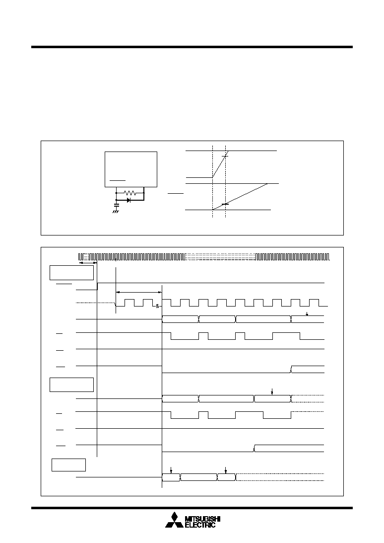
When the supply voltage is in the range where operation is guaranteed, a reset is effected by holding the
reset pin level "L" (0.2V
CC
max.) for at least 20 cycles. When the reset pin level is then returned to the "H"
level while main clock is stable, the reset status is cancelled and program execution resumes from the
address in the reset vector table.
Figure 1.5.1 shows the example reset circuit. Figure 1.5.2 shows the reset sequence.
Figure 1.5.1. Example reset circuit
BCLK
Address
Address
Address
Microprocessor
mode BYTE = "H"
Microprocessor
mode BYTE = "L"
Content of reset vector
Single chip
mode
BCLK 24cycles
FFFFC
16
FFFFD
16
FFFFE
16
Content of reset vector
FFFFC
16
FFFFE
16
Content of reset vector
FFFFE
16
X
IN
RESET
RD
WR
CS0
RD
WR
CS0
FFFFC
16
More than 20 cycles are needed
RESET
V
CC
0.8V
RESET
V
CC
0V
0V
5V
5V
4.0V
Example when V
CC
= 5V
.

Mitsubishi microcomputers
M16C / 62A Group
SINGLE-CHIP 16-BIT CMOS MICROCOMPUTER
Reset
15
____________
Table 1.5.1 shows the statuses of the other pins while the RESET pin level is "L". Figures 1.5.3 and 1.5.4
show the internal status of the microcomputer immediately after the reset is cancelled.
____________
Table 1.5.1. Pin status when RESET pin level is "L"
Status
CNV
SS
= V
CC
CNV
SS
= V
SS
BYTE = V
SS
BYTE = V
CC
Pin name
P0
P1
P2, P3, P4
0
to P4
3
P4
4
P4
5
to P4
7
P5
0
P5
1
P5
2
P5
3
P5
4
P5
5
P5
6
P5
7
P6, P7, P8
0
to P8
4
,
P8
6
, P8
7
, P9, P10
Input port (floating)
Input port (floating)
Input port (floating)
Input port (floating)
Input port (floating)
Input port (floating)
Input port (floating)
Input port (floating)
Input port (floating)
Input port (floating)
Input port (floating)
Input port (floating)
Input port (floating)
Input port (floating)
Data input (floating)
Data input (floating)
Address output (undefined)
BCLK output
ALE output ("L" level is output)
CS0 output ("H" level is output)
WR output ("H" level is output)
RD output ("H" level is output)
RDY input (floating)
Input port (floating)
BCLK output
BHE output (undefined)
HLDA output (The output value
depends on the input to the
HOLD pin)
HOLD input (floating)
Data input (floating)
Address output (undefined)
CS0 output ("H" level is output)
Input port (floating)
(pull-up resistor is on)
Input port (floating)
Input port (floating)
RDY input (floating)
ALE output ("L" level is output)
HOLD input (floating)
HLDA output (The output value
depends on the input to the
HOLD pin)
RD output ("H" level is output)
BHE output (undefined)
WR output ("H" level is output)
Input port (floating)
(pull-up resistor is on)

Mitsubishi microcomputers
M16C / 62A Group
SINGLE-CHIP 16-BIT CMOS MICROCOMPUTER
Reset
16
Figure 1.5.3. Device's internal status after a reset is cleared
x : Nothing is mapped to this bit
? : Undefined
The content of other registers and RAM is undefined when the microcomputer is reset. The initial values must therefore be set.
Note 1: When the V
CC
level is applied to the CNV
SS
pin, it is 03
16
at a reset.
Note 2: "00
16
" is read out when set bit 7 (SDDS) of the UART2 special mode register ( address 0377
16
) to "1".
(1)
(0004
16
)∑∑∑
Processor mode register 0 (Note 1)
00
16
(2)
(0005
16
)∑∑∑
Processor mode register 1
0
0
0
(3)
(0006
16
)∑∑∑
System clock control register 0
1
0
0
0
0
1
0
0
(4)
(0007
16
)∑∑∑
System clock control register 1
0
0
0
1
0
0
0
0
(5)
(0008
16
)∑∑∑
Chip select control register
0
0
0
0
0
0
1
0
(6)
(0009
16
)∑∑∑
Address match interrupt enable register
0
0
(7) Protect register
(000A
16
)∑∑∑
0
0
0
(9)
(000F
16
)∑∑∑
Watchdog timer control register
0
0
?
0
? ? ? ?
(11)
(0014
16
)∑∑∑
Address match interrupt register 1
(0015
16
)∑∑∑
(0016
16
)∑∑∑
0
00
16
00
16
0 0 0
(12)
(002C
16
)∑∑∑
DMA0 control register
0 0 0 0 0 ? 0 0
(13)
(003C
16
)∑∑∑
DMA1 control register
0 0 0 0 0 ? 0 0
(21)
(004B
16
)∑∑∑
DMA0 interrupt control register
? 0 0 0
(22)
(004C
16
)∑∑∑
DMA1 interrupt control register
? 0 0 0
(23)
(004D
16
)∑∑∑
Key input interrupt control register
? 0 0 0
(20)
(004A
16
)∑∑∑
Bus collision detection interrupt
control register
0 0 0
?
(8)
(0010
16
)∑∑∑
Address match interrupt register 0
(0011
16
)∑∑∑
(0012
16
)∑∑∑
0
00
16
00
16
0 0 0
(10)
(14)
(0044
16
)∑∑∑
INT3 interrupt control register
0 0 ? 0 0 0
(15)
(0045
16
)∑∑∑
Timer B5 interrupt control register
? 0 0 0
(16)
(0046
16
)∑∑∑
Timer B4 interrupt control register
? 0 0 0
(17)
(0047
16
)∑∑∑
Timer B3 interrupt control register
? 0 0 0
(18)
(0048
16
)∑∑∑
SI/O4 interrupt control register
0 0 ? 0 0 0
(19)
(0049
16
)∑∑∑
SI/O3 interrupt control register
0 0 ? 0 0 0
(24)
A-D conversion interrupt control register
(25)
(26)
UART2 transmit interrupt control register
UART2 receive interrupt control register
(004E
16
)∑∑∑
? 0 0 0
(004F
16
)∑∑∑
(0050
16
)∑∑∑
? 0 0 0
? 0 0 0
0
0
0
(27)
(28)
(29)
(30)
UART0 transmit interrupt control register
UART0 receive interrupt control register
UART1 transmit interrupt control register
UART1 receive interrupt control register
(31)
(32)
(33)
(34)
(35)
(36)
(37)
Timer A0 interrupt control register
Timer A1 interrupt control register
Timer A2 interrupt control register
Timer A3 interrupt control register
Timer A4 interrupt control register
Timer B0 interrupt control register
Timer B1 interrupt control register
(38)
Timer B2 interrupt control register
(39)
INT0 interrupt control register
(40)
INT1 interrupt control register
(41)
INT2 interrupt control register
(45)
Three-phase output buffer register 0
(46)
Three-phase output buffer register 1
Three-phase PWM control register 0
(43)Three-phase PWM control register 1
(44)
(42)
Timer B3,4,5 count start flag
(47)
Timer B3 mode register
(48)
Timer B4 mode register
(49)
Timer B5 mode register
(50)
Interrupt cause select register
00
16
UART2 transmit/receive control register 1
UART2 transmit/receive control register 0
(0378
16
)∑∑∑
(037D
16
)∑∑∑
(037C
16
)∑∑∑
00
16
0 0 0
0 0 0 0 1
0 1 0
0 0 0 0 0
(57)
UART2 transmit/receive mode register
(55)
(56)
(52)
SI/O4 control register
(54) UART2 special mode register
(0051
16
)∑∑∑
(0052
16
)∑∑∑
(0053
16
)∑∑∑
(0054
16
)∑∑∑
(0055
16
)∑∑∑
(0056
16
)∑∑∑
(0057
16
)∑∑∑
(0058
16
)∑∑∑
(0059
16
)∑∑∑
(005A
16
)∑∑∑
(005B
16
)∑∑∑
(005C
16
)∑∑∑
(005D
16
)∑∑∑
(005E
16
)∑∑∑
(005F
16
)∑∑∑
(034A
16
)∑∑∑
(034B
16
)∑∑∑
(0348
16
)∑∑∑
(0349
16
)∑∑∑
(0340
16
)∑∑∑
(035B
16
)∑∑∑
(035C
16
)∑∑∑
(035D
16
)∑∑∑
(035F
16
)∑∑∑
(0366
16
)∑∑∑
(0377
16
)∑∑∑
(0362
16
)∑∑∑
SI/O3 control register
? 0 0 0
? 0 0 0
? 0 0 0
? 0 0 0
? 0 0 0
? 0 0 0
? 0 0 0
? 0 0 0
? 0 0 0
? 0 0 0
? 0 0 0
? 0 0 0
? 0 0 0
0 0
? 0 0 0
0 0
? 0 0 0
0 0
00
16
00
16
00
16
00
16
0 0 ?
0 0 0 0
0 0 ?
0 0 0 0
0 0 ?
0 0 0 0
40
16
00
16
40
16
(51)
0 0 0
(53) UART2 special mode register 2
(0376
16
)∑∑∑
00
16
UART2 special mode register 3 (Note 2)
(0375
16
)∑∑∑
?

Mitsubishi microcomputers
M16C / 62A Group
SINGLE-CHIP 16-BIT CMOS MICROCOMPUTER
Reset
17
(0383
16
)∑∑∑
Trigger select flag
(0384
16
)∑∑∑
Up-down flag
(62)
(61)
(0396
16
)∑∑∑
Timer A0 mode register
(63)
(0397
16
)∑∑∑
Timer A1 mode register
(64)
(0398
16
)∑∑∑
Timer A2 mode register
(67)
(039B
16
)∑∑∑
Timer B0 mode register
(68)
(039C
16
)∑∑∑
Timer B1 mode register
(69)
(039D
16
)∑∑∑
Timer B2 mode register
(70)
(65)
(0399
16
)∑∑∑
Timer A3 mode register
(66)
(039A
16
)∑∑∑
Timer A4 mode register
(0382
16
)∑∑∑
One-shot start flag
(60)
00
16
00
16
0
00
16
00
16
00
16
00
16
00
16
0 ?
0 0 0 0
0 0 ?
0 0 0 0
0 0 ?
0 0 0 0
(03AC
16
)∑∑∑
UART1 transmit/receive control register 0
(75)
(03AD
16
)∑∑∑
UART1 transmit/receive control register 1
(76)
(03B0
16
)∑∑∑
UART transmit/receive control register 2
(77)
0
(03A0
16
)∑∑∑
UART0 transmit/receive mode register
(71)
(03A4
16
)∑∑∑
UART0 transmit/receive control register 0
(72)
(03A5
16
)∑∑∑
UART0 transmit/receive control register 1
(73)
00
16
0 0 0
1 0 0 0
0 0 0
0 0 1 0
0
0
(03A8
16
)∑∑∑
UART1 transmit/receive mode register
(74)
00
16
0 0 0
1 0 0 0
0 0 0
0 0 1 0
0
0
0
0 0 0 0
0
(03D7
16
)∑∑∑
A-D control register 1
00
16
0
0
0
0
0 0 0
Count start flag
(0380
16
)∑∑∑
00
16
0
(0381
16
)∑∑∑
Clock prescaler reset flag
(58)
(59)
x : Nothing is mapped to this bit
? : Undefined
The content of other registers and RAM is undefined when the microcomputer is reset. The initial values
must therefore be set.
Note1: When the V
CC
level is applied to the CNV
SS
pin, it is 02
16
at a reset.
Note2: This register is only exist in flash memory version.
(03E2
16
)∑∑∑
Port P0 direction register
(84)
(03E3
16
)∑∑∑
Port P1 direction register
(85)
(03E6
16
)∑∑∑
Port P2 direction register
(86)
(03E7
16
)∑∑∑
Port P3 direction register
(87)
(03EA
16
)∑∑∑
Port P4 direction register
(88)
(03EB
16
)∑∑∑
Port P5 direction register
(89)
(03EE
16
)∑∑∑
Port P6 direction register
(90)
(03EF
16
)∑∑∑
Port P7 direction register
(91)
(03F2
16
)∑∑∑
Port P8 direction register
(92)
(03F3
16
)∑∑∑
Port P9 direction register
(93)
(03F6
16
)∑∑∑
Port P10 direction register
(94)
(03FC
16
)∑∑∑
Pull-up control register 0
(95)
(03FD
16
)∑∑∑
Pull-up control register 1(Note1)
(96)
(03FE
16
)∑∑∑
Pull-up control register 2
(97)
Port control register
(98)
00
16
00
16
00
16
00
16
00
16
00
16
00
16
00
16
00
16
00
16
00
16
00
16
00
16
00
16
0 0
0
0
0
0 0
(03DC
16
)∑∑∑
D-A control register
(83)
00
16
Frame base register (FB)
(101)
Address registers (A0/A1)
(100)
Interrupt table register (INTB)
(102)
User stack pointer (USP)
(103)
Interrupt stack pointer (ISP)
(104)
Static base register (SB)
(105)
Flag register (FLG)
(106)
0000
16
0000
16
00000
16
0000
16
0000
16
0000
16
0000
16
Data registers (R0/R1/R2/R3)
(99)
0000
16
(03FF
16
)∑∑∑
(03B6
16
)∑∑∑
Flash memory control register 1 (Note2)
(78)
0
(107)
(03B7
16
)∑∑∑
Flash memory control register 0 (Note2)
(03BA
16
)∑∑∑
DMA1 cause select register
00
16
(03D4
16
)∑∑∑
A-D control register 2
(80)
(03D6
16
)∑∑∑
A-D control register 0
(81)
(82)
0
0 0 0
0 ? ? ?
0
0 0 0 0
(03B8
16
)∑∑∑
DMA0 cause select register
(79)
00
16
0
0 0 0 1
0
? ? ? ?
? ? ?
(108)
Figure 1.5.4. Device's internal status after a reset is cleared

Mitsubishi microcomputers
M16C / 62A Group
SINGLE-CHIP 16-BIT CMOS MICROCOMPUTER
SFR
18
Figure 1.6.1. Location of peripheral unit control registers (1)
0000
16
0001
16
0002
16
0003
16
0004
16
0005
16
0006
16
0007
16
0008
16
0009
16
000A
16
000B
16
000C
16
000D
16
000E
16
000F
16
0010
16
0011
16
0012
16
0013
16
0014
16
0015
16
0016
16
0017
16
0018
16
0019
16
001A
16
001B
16
001C
16
001D
16
001E
16
001F
16
0020
16
0021
16
0022
16
0023
16
0024
16
0025
16
0026
16
0027
16
0028
16
0029
16
002A
16
002B
16
002C
16
002D
16
002E
16
002F
16
0030
16
0031
16
0032
16
0033
16
0034
16
0035
16
0036
16
0037
16
0038
16
0039
16
003A
16
003B
16
003C
16
003D
16
003E
16
003F
16
0040
16
0041
16
0042
16
0043
16
0044
16
0045
16
0046
16
0047
16
0048
16
0049
16
004A
16
004B
16
004C
16
004D
16
004E
16
004F
16
0050
16
0051
16
0052
16
0053
16
0054
16
0055
16
0056
16
0057
16
0058
16
0059
16
005A
16
005B
16
005C
16
005D
16
005E
16
005F
16
0060
16
0061
16
0062
16
0063
16
0064
16
0065
16
032A
16
032B
16
032C
16
032D
16
032E
16
032F
16
0330
16
0331
16
0332
16
0333
16
0334
16
0335
16
0336
16
0337
16
0338
16
0339
16
033A
16
033B
16
033C
16
033D
16
033E
16
033F
16
DMA0 control register (DM0CON)
DMA0 source pointer (SAR0)
DMA0 transfer counter (TCR0)
DMA1 control register (DM1CON)
DMA1 source pointer (SAR1)
DMA1 transfer counter (TCR1)
DMA1 destination pointer (DAR1)
Watchdog timer start register (WDTS)
Watchdog timer control register (WDC)
Processor mode register 0 (PM0)
Address match interrupt register 0 (RMAD0)
Address match interrupt register 1 (RMAD1)
Chip select control register (CSR)
System clock control register 0 (CM0)
System clock control register 1 (CM1)
Address match interrupt enable register (AIER)
Protect register (PRCR)
Processor mode register 1(PM1)
DMA0 destination pointer (DAR0)
Timer A1 interrupt control register (TA1IC)
UART0 transmit interrupt control register (S0TIC)
Timer A0 interrupt control register (TA0IC)
Timer A2 interrupt control register (TA2IC)
UART0 receive interrupt control register (S0RIC)
UART1 transmit interrupt control register (S1TIC)
UART1 receive interrupt control register (S1RIC)
DMA1 interrupt control register (DM1IC)
DMA0 interrupt control register (DM0IC)
Key input interrupt control register (KUPIC)
A-D conversion interrupt control register (ADIC)
Bus collision detection interrupt control register (BCNIC)
UART2 transmit interrupt control register (S2TIC)
UART2 receive interrupt control register (S2RIC)
INT1 interrupt control register (INT1IC)
Timer B0 interrupt control register (TB0IC)
Timer B2 interrupt control register (TB2IC)
Timer A3 interrupt control register (TA3IC)
INT2 interrupt control register (INT2IC)
INT0 interrupt control register (INT0IC)
Timer B1 interrupt control register (TB1IC)
Timer A4 interrupt control register (TA4IC)
INT3 interrupt control register (INT3IC)
Timer B5 interrupt control register (TB5IC)
Timer B4 interrupt control register (TB4IC)
Timer B3 interrupt control register (TB3IC)
SI/O4 interrupt control register (S4IC)
INT5 interrupt control register (INT5IC)
SI/O3 interrupt control register (S3IC)
INT4 interrupt control register (INT4IC)
Note 1: Locations in the SFR area where nothing is allocated are reserved areas. Do not access these areas for read or write.

Mitsubishi microcomputers
M16C / 62A Group
SINGLE-CHIP 16-BIT CMOS MICROCOMPUTER
SFR
19
Figure 1.6.2. Location of peripheral unit control registers (2)
0380
16
0381
16
0382
16
0383
16
0384
16
0385
16
0386
16
0387
16
0388
16
0389
16
038A
16
038B
16
038C
16
038D
16
038E
16
038F
16
0390
16
0391
16
0392
16
0393
16
0394
16
0395
16
0396
16
0397
16
0398
16
0399
16
039A
16
039B
16
039C
16
039D
16
039E
16
039F
16
03A0
16
03A1
16
03A2
16
03A3
16
03A4
16
03A5
16
03A6
16
03A7
16
03A8
16
03A9
16
03AA
16
03AB
16
03AC
16
03AD
16
03AE
16
03AF
16
03B0
16
03B1
16
03B2
16
03B3
16
03B4
16
03B5
16
03B6
16
03B7
16
03B8
16
03B9
16
03BA
16
03BB
16
03BC
16
03BD
16
03BE
16
03BF
16
0340
16
0341
16
0342
16
0343
16
0344
16
0345
16
0346
16
0347
16
0348
16
0349
16
034A
16
034B
16
034C
16
034D
16
034E
16
034F
16
0350
16
0351
16
0352
16
0353
16
0354
16
0355
16
0356
16
0357
16
0358
16
0359
16
035A
16
035B
16
035C
16
035D
16
035E
16
035F
16
0360
16
0361
16
0362
16
0363
16
0364
16
0365
16
0366
16
0367
16
0368
16
0369
16
036A
16
036B
16
036C
16
036D
16
036E
16
036F
16
0370
16
0371
16
0372
16
0373
16
0374
16
0375
16
0376
16
0377
16
0378
16
0379
16
037A
16
037B
16
037C
16
037D
16
037E
16
037F
16
Timer A1-1 register (TA11)
Timer A2-1 register (TA21)
Dead time timer(DTT)
Timer B2 interrupt occurrence frequency set counter(ICTB2)
Three-phase PWM control register 0(INVC0)
Three-phase PWM control register 1(INVC1)
Three-phase output buffer register 0(IDB0)
Three-phase output buffer register 1(IDB1)
Timer B3 register (TB3)
Timer B4 register (TB4)
Timer B5 register (TB5)
Timer B3, 4, 5 count start flag (TBSR)
Timer B3 mode register (TB3MR)
Timer B4 mode register (TB4MR)
Timer B5 mode register (TB5MR)
Interrupt cause select register (IFSR)
Timer A0 (TA0)
Timer A1 (TA1)
Timer A2 (TA2)
Timer B0 (TB0)
Timer B1 (TB1)
Timer B2 (TB2)
Count start flag (TABSR)
One-shot start flag (ONSF)
Timer A0 mode register (TA0MR)
Timer A1 mode register (TA1MR)
Timer A2 mode register (TA2MR)
Timer B0 mode register (TB0MR)
Timer B1 mode register (TB1MR)
Timer B2 mode register (TB2MR)
Up-down flag (UDF)
Timer A3 (TA3)
Timer A4 (TA4)
Timer A3 mode register (TA3MR)
Timer A4 mode register (TA4MR)
Trigger select register (TRGSR)
Clock prescaler reset flag (CPSRF)
UART0 transmit/receive mode register (U0MR)
UART0 transmit buffer register (U0TB)
UART0 receive buffer register (U0RB)
UART1 transmit/receive mode register (U1MR)
UART1 transmit buffer register (U1TB)
UART1 receive buffer register (U1RB)
UART0 bit rate generator (U0BRG)
UART0 transmit/receive control register 0 (U0C0)
UART0 transmit/receive control register 1 (U0C1)
UART1 bit rate generator (U1BRG)
UART1 transmit/receive control register 0 (U1C0)
UART1 transmit/receive control register 1 (U1C1)
DMA1 request cause select register (DM1SL)
DMA0 request cause select register (DM0SL)
CRC data register (CRCD)
CRC input register (CRCIN)
SI/O3
transmit/receive register
(S3TRR)
SI/O4
transmit/receive register
(S4TRR)
SI/O3 control register (S3C)
SI/O3
bit rate generator
(S3BRG)
SI/O4
bit rate generator
(S4BRG)
SI/O4 control register (S4C)
UART2 special mode register (U2SMR)
UART2 receive buffer register (U2RB)
UART2 transmit buffer register (U2TB)
UART2 transmit/receive control register 0 (U2C0)
UART2 transmit/receive mode register (U2MR)
UART2 transmit/receive control register 1 (U2C1)
UART2 bit rate generator (U2BRG)
UART transmit/receive control register 2 (UCON)
Timer A4-1 register (TA41)
UART2 special mode register 2(U2SMR2)
Note 1: This register is only exist in flash memory version.
Note 2: Locations in the SFR area where nothing is allocated are reserved areas. Do not access these areas for
read or write.
Flash memory control register 0 (FMR0) (Note1)
Flash memory control register 1 (FMR1) (Note1)
UART2 special mode register 3(U2SMR3)

Mitsubishi microcomputers
M16C / 62A Group
SINGLE-CHIP 16-BIT CMOS MICROCOMPUTER
SFR
20
Figure 1.6.3. Location of peripheral unit control registers (3)
03C0
16
03C1
16
03C2
16
03C3
16
03C4
16
03C5
16
03C6
16
03C7
16
03C8
16
03C9
16
03CA
16
03CB
16
03CC
16
03CD
16
03CE
16
03CF
16
03D0
16
03D1
16
03D2
16
03D3
16
03D4
16
03D5
16
03D6
16
03D7
16
03D8
16
03D9
16
03DA
16
03DB
16
03DC
16
03DD
16
03DE
16
03DF
16
03E0
16
03E1
16
03E2
16
03E3
16
03E4
16
03E5
16
03E6
16
03E7
16
03E8
16
03E9
16
03EA
16
03EB
16
03EC
16
03ED
16
03EE
16
03EF
16
03F0
16
03F1
16
03F2
16
03F3
16
03F4
16
03F5
16
03F6
16
03F7
16
03F8
16
03F9
16
03FA
16
03FB
16
03FC
16
03FD
16
03FE
16
03FF
16
A-D register 7 (AD7)
A-D register 0 (AD0)
A-D register 1 (AD1)
A-D register 2 (AD2)
A-D register 3 (AD3)
A-D register 4 (AD4)
A-D register 5 (AD5)
A-D register 6 (AD6)
Port P0 (P0)
Port P0 direction register (PD0)
Port P1 (P1)
Port P1 direction register (PD1)
Port P2 (P2)
Port P2 direction register (PD2)
Port P3 (P3)
Port P3 direction register (PD3)
Port P4 (P4)
Port P4 direction register (PD4)
Port P5 (P5)
Port P5 direction register (PD5)
Port P6 (P6)
Port P6 direction register (PD6)
Port P7 (P7)
Port P7 direction register (PD7)
Port P8 (P8)
Port P8 direction register (PD8)
Port P9 (P9)
Port P9 direction register (PD9)
Port P10 (P10)
Port P10 direction register (PD10)
Pull-up control register 0 (PUR0)
Pull-up control register 1 (PUR1)
Pull-up control register 2 (PUR2)
A-D control register 0 (ADCON0)
A-D control register 1 (ADCON1)
D-A register 0 (DA0)
D-A register 1 (DA1)
D-A control register (DACON)
A-D control register 2 (ADCON2)
Port control register (PCR)
Note : Locations in the SFR area where nothing is allocated are reserved
areas. Do not access these areas for read or write.

Mitsubishi microcomputers
M16C / 62A Group
SINGLE-CHIP 16-BIT CMOS MICROCOMPUTER
Software Reset
21
Software Reset
Writing "1" to bit 3 of the processor mode register 0 (address 0004
16
) applies a (software) reset to the
microcomputer. A software reset has the same effect as a hardware reset. The contents of internal RAM
are preserved.
Software Reset
Processor Mode
(1) Types of Processor Mode
One of three processor modes can be selected: single-chip mode, memory expansion mode, and micro-
processor mode. The functions of some pins, the memory map, and the access space differ according to
the selected processor mode.
∑ Single-chip mode
In single-chip mode, only internal memory space (SFR, internal RAM, and internal ROM) can be
accessed. However, after the reset has been released and the operation of shifting from the micropro-
cessor mode has started ("H" applied to the CNV
SS
pin), the internal ROM area cannot be accessed
even if the CPU shifts to the single-chip mode.
Ports P0 to P10 can be used as programmable I/O ports or as I/O ports for the internal peripheral
functions.
∑ Memory expansion mode
In memory expansion mode, external memory can be accessed in addition to the internal memory
space (SFR, internal RAM, and internal ROM). However, after the reset has been released and the
operation of shifting from the microprocessor mode has started ("H" applied to the CNV
SS
pin), the
internal ROM area cannot be accessed even if the CPU shifts to the memory expansion mode.
In this mode, some of the pins function as the address bus, the data bus, and as control signals. The
number of pins assigned to these functions depends on the bus and register settings. (See "Bus
Settings" for details.)
∑ Microprocessor mode
In microprocessor mode, the SFR, internal RAM, and external memory space can be accessed. The
internal ROM area cannot be accessed.
In this mode, some of the pins function as the address bus, the data bus, and as control signals. The
number of pins assigned to these functions depends on the bus width and register settings. (See "Bus
Settings" for details.)
(2) Setting Processor Modes
The processor mode is set using the CNV
SS
pin and the processor mode bits (bits 1 and 0 at address
0004
16
). Do not set the processor mode bits to "10
2
".
Regardless of the level of the CNV
SS
pin, changing the processor mode bits selects the mode. Therefore,
never change the processor mode bits when changing the contents of other bits. Do not change the
processor mode bits simultaneously with other bits when changing the processor mode bits "01
2
" or
"11
2
". Change the processor mode bits after changing the other bits. Also do not attempt to shift to or from
the microprocessor mode within the program stored in the internal ROM area.
∑ Applying V
SS
to CNV
SS
pin
The microcomputer begins operation in single-chip mode after being reset. Memory expansion mode
is selected by writing "01
2
" to the processor mode bits.
∑ Applying V
CC
to CNV
SS
pin
The microcomputer starts to operate in microprocessor mode after being reset.

Mitsubishi microcomputers
M16C / 62A Group
SINGLE-CHIP 16-BIT CMOS MICROCOMPUTER
Processor Mode
22
Figure 1.7.1. Processor mode register 0 and 1
Processor mode register 0 (Note 1)
Symbol
Address
When reset
PM0
0004
16
00
16
(Note 2)
Bit name
Function
Bit symbol
W
R
b7
b6
b5
b4
b3
b2
b1
b0
0 0: Single-chip mode
0 1: Memory expansion mode
1 0: Do not set
1 1: Microprocessor mode
b1 b0
PM03
PM01
PM00
Processor mode bit
PM02
R/W mode select bit
0 : RD,BHE,WR
1 : RD,WRH,WRL
Software reset bit
The device is reset when this bit is set
to "1". The value of this bit is "0" when
read.
PM04
0 0 : Multiplexed bus is not used
0 1 : Allocated to CS2 space
1 0 : Allocated to CS1 space
1 1 : Allocated to entire space (Note4)
b5 b4
Multiplexed bus space
select bit
PM05
PM06
PM07
Port P4
0
to P4
3
function
select bit (Note 3)
0 : Address output
1 : Port function
(Address is not output)
BCLK output disable bit
0 : BCLK is output
1 : BCLK is not output
(Pin is left floating)
Note 1: Set bit 1 of the protect register (address 000A
16
) to "1" when writing new
values to this register.
Note 2: If the V
CC
voltage is applied to the CNV
SS
, the value of this register when
reset is 03
16
. (PM00 and PM01 both are set to "1".)
Note 3: Valid in microprocessor and memory expansion modes.
Note 4: If the entire space is of multiplexed bus in memory expansion mode, choose an 8-
bit width.The processor operates using the separate bus after reset is revoked, so the entire
space multiplexed bus cannot be chosen in microprocessor mode.
P3
1
to P3
7
become a port if the entire space multiplexed bus is chosen, so only 256 bytes can
be used in each chip select.
Processor mode register 1 (Note 1)
Symbol
Address
When reset
PM1
0005
16
00000XX0
2
Bit name
Function
Bit symbol
W
R
b7
b6
b5
b4
b3
b2
b1
b0
Nothing is assigned.
In an attempt to write to these bits, write "0". The value, if read, turns
out to be
indeterminate.
Reserved bit
Must always be set to "0"
0
Note 1: Set bit 1 of the protect register (address 000A
16
) to "1" when writing new values to this register.
Note 2: When the reset is revoked, this bit is set to "0". To expand the internal area, set this bit to "1"
in user program. And the top of user program must be allocated to D0000
16
or subsequent
address.
PM17
Wait bit
0 : No wait state
1 : Wait state inserted
Reserved bit
Must always be set to "0"
0
Internal reserved area
expansion bit (Note 2)
PM13
0: The internal RAM area is 15 kbytes
or less and the internal ROM area is
192 kbytes or less
1: Expands the internal RAM area
and internal ROM area to over 15
kbytes and to over 192 kbytes
respectively. (Note 2)
0 0
Reserved bit
Must always be set to "0"
Reserved bit
Must always be set to "0"
Figure 1.7.1 shows the processor mode register 0 and 1.
Figure 1.7.2 shows the memory maps applicable for each of the modes.

Mitsubishi microcomputers
M16C / 62A Group
SINGLE-CHIP 16-BIT CMOS MICROCOMPUTER
Processor Mode
23
Single-chip mode
SFR area
Internal
RAM area
Inhibited
Internal
ROM area
Microprocessor mode
SFR area
Internal
RAM area
External
area
Internally
reserved area
00000
16
00400
16
XXXXX
16
YYYYY
16
FFFFF
16
D0000
16
External area :
Accessing this area allows the user to
access a device connected externally
to the microcomputer.
04000
16
Memory expansion mode
SFR area
Internal
RAM area
External
area
Internal
ROM area
Internally
reserved area
Internally
reserved area
Note : These memory maps show an instance in which PM13 is set to 0; but in the case of products in which the
internal RAM and the internal ROM are expanded to over 15 Kbytes and 192 Kbytes, respectively, they show
an instance in which PM13 is set to 1.
Address YYYYY
16
3K bytes
00FFF
16
053FF
16
017FF
16
013FF
16
Address XXXXX
16
ROM size
02BFF
16
5K bytes
4K bytes
10K bytes
20K bytes
RAM size
32K bytes
C0000
16
E8000
16
F0000
16
E0000
16
96K bytes
64K bytes
128K bytes
256K bytes
F8000
16
Figure 1.7.2. Memory maps in each processor mode (without memory area expansion, normal mode)
Internal Reserved Area Expansion Bit (PM13)
This bit expands the internal RAM area and the internal ROM area, and changes the chip select area. In
M30624MGA/FGA, for example, to set this bit to "1" expands the internal RAM area and the internal ROM
area to 20 Kbytes and 256 Kbytes respectively. Refer to Figure 1.7.3 for the chip select area. When the
reset is revoked, this bit is set to "0". To expand the internal area, set this bit to "1" in user program. And
the top of user program must be allocated to D0000
16
or subsequent address.
In the case of the product in which the internal ROM is 192 Kbytes or less and the internal RAM is 15
Kbytes or less, set this bit to "0" when this product is used in the memory expansion mode or the micro-
processor mode. When the product is used in the single chip mode, the internal area is not expanded and
any action is not affected, even if this bit is set to "1".

Mitsubishi microcomputers
M16C / 62A Group
SINGLE-CHIP 16-BIT CMOS MICROCOMPUTER
Processor Mode
24
SFR area
(1K bytes)
Internal RAM area
(15K bytes)
External area
00000
16
00400
16
FFFFF
16
D0000
16
08000
16
Internal RAM area
(15K bytes)
External area
Internal ROM area
(192K bytes)
CS3
(16K bytes)
CS2
(128K bytes)
CS1
(32K bytes)
CS0
Memory expansion mode
: 640K bytes
Microprocessor mode
: 832K bytes
28000
16
30000
16
04000
16
Internal reserved area expansion bit="0"
SFR area
(1K bytes)
After reset
SFR area
(1K bytes)
00000
16
00400
16
FFFFF
16
C0000
16
08000
16
Internal RAM area
(20K bytes)
Internal ROM area
(256K bytes)
CS3
(8K bytes)
CS2
(128K bytes)
CS1
(32K bytes)
CS0
Memory expansion mode
: 576K bytes
Microprocessor mode
: 832K bytes
28000
16
30000
16
05400
16
Internal reserved area expansion bit="1" (Note)
SFR area
(1K bytes)
After reset, and set the
Internal reserved area expansion bit to "1"
06000
16
BFFFF
16
CFFFF
16
Note: When the reset is revoked, this bit is set to "0". Therefore, the top
of the user program must be allocated to D0000
16
or subsequent address.
Memory expansion
mode
Microprocessor
mode
Memory expansion
mode
Microprocessor
mode
Internal RAM area
(20K bytes)
Internal reserved area
External area
External area
Internal reserved area
Figure 1.7.3. Memory location and chip select area in each processor mode
Figure 1.7.3 shows the memory maps and the chip selection areas effected by PM13 (the internal re-
served area expansion bit) in each processor mode for the product having an internal RAM of more than
15K bytes and a ROM of more than 192K bytes.

Mitsubishi microcomputers
M16C / 62A Group
SINGLE-CHIP 16-BIT CMOS MICROCOMPUTER
Bus Settings
25
Bus Settings
The BYTE pin and bits 4 to 6 of the processor mode register 0 (address 0004
16
) are used to change the bus settings.
Table 1.8.1 shows the factors used to change the bus settings.
Bus setting
Switching factor
Switching external address bus width
Bit 6 of processor mode register 0
Switching external data bus width
BYTE pin
Switching between separate and multiplex bus
Bits 4 and 5 of processor mode register 0
(1) Selecting external address bus width
The address bus width for external output in the 1M bytes of address space can be set to 16 bits (64K
bytes address space) or 20 bits (1M bytes address space). When bit 6 of the processor mode register 0
is set to "1", the external address bus width is set to 16 bits, and P2 and P3 become part of the address
bus. P4
0
to P4
3
can be used as programmable I/O ports. When bit 6 of processor mode register 0 is set
to "0", the external address bus width is set to 20 bits, and P2, P3, and P4
0
to P4
3
become part of the
address bus.
(2) Selecting external data bus width
The external data bus width can be set to 8 or 16 bits. (Note, however, that only the separate bus can be
set.) When the BYTE pin is "L", the bus width is set to 16 bits; when "H", it is set to 8 bits. (The internal bus
width is permanently set to 16 bits.) While operating, fix the BYTE pin either to "H" or to "L".
(3) Selecting separate/multiplex bus
The bus format can be set to multiplex or separate bus using bits 4 and 5 of the processor mode register 0.
∑ Separate bus
In this mode, the data and address are input and output separately. The data bus can be set using the
BYTE pin to be 8 or 16 bits. When the BYTE pin is "H", the data bus is set to 8 bits and P0 functions as
the data bus and P1 as a programmable I/O port. When the BYTE pin is "L", the data bus is set to 16
bits and P0 and P1 are both used for the data bus.
When the separate bus is used for access, a software wait can be selected.
∑ Multiplex bus
In this mode, data and address I/O are time multiplexed. With the BYTE pin = "H", the 8 bits from D
0
to
D
7
are multiplexed with A
0
to A
7
.
With the BYTE pin = "L", the 8 bits from D
0
to D
7
are multiplexed with A
1
to A
8
. D
8
to D
15
are not
multiplexed. In this case, the external devices connected to the multiplexed bus are mapped to the
microcomputer's even addresses (every 2nd address). To access these external devices, access the
even addresses as bytes.
The ALE signal latches the address. It is output from P5
6
.
Before using the multiplex bus for access, be sure to insert a software wait.
If the entire space is of multiplexed bus in memory expansion mode, choose an 8-bit width.
The processor operates using the separate bus after reset is revoked, so the entire space multiplexed
bus cannot be chosen in microprocessor mode.
P3
1
to P3
7
become a port if the entire space multiplexed bus is chosen, so only 256 bytes can be used
in each chip select.
Table 1.8.1. Factors for switching bus settings

Mitsubishi microcomputers
M16C / 62A Group
SINGLE-CHIP 16-BIT CMOS MICROCOMPUTER
Bus Settings
26
P5
6
I/O port
ALE
ALE
ALE
ALE
ALE
P5
7
I/O port
RDY
RDY
RDY
RDY
RDY
P0
0
to P0
7
I/O port
Data bus
Data bus
Data bus
Data bus
I/O port
Either CS1 or CS2 is for
multiplexed bus and others
are for separate bus
(separate bus)
multiplexed
bus for the
entire
space
Single-chip
mode
Memory expansion mode/microprocessor modes
Memory
expansion mode
Data bus width
BYTE pin level
Port P4
0
to P4
3
function select bit = 0
"01", "10"
"00"
"11" (Note 1)
8 bit
"H"
8 bits
"H"
16 bits
"L"
8 bits
"H"
16 bits
"L"
Note 1: If the entire space is of multiplexed bus in memory expansion mode, choose an 8-bit width.
The processor operates using the separate bus after reset is revoked, so the entire space multiplexed bus cannot be
chosen in microprocessor mode.
P3
1
to P3
7
become a port if the entire space multiplexed bus is chosen, so only 256 bytes can be used
in each chip select.
Note 2: Address bus when in separate bus mode.
Processor mode
Multiplexed bus
space select bit
CS (chip select) or programmable I/O port
(For details, refer to "Bus control")
Outputs RD, WRL, WRH, and BCLK or RD, BHE, WR, and BCLK
(For details, refer to "Bus control")
Port P4
0
to P4
3
function select bit = 1
P1
0
to P1
7
I/O port
I/O port
Data bus
I/O port
Data bus
I/O port
P2
1
to P2
7
I/O port
Address bus
Address bus
Address bus
Address bus
Address bus
/data bus
(Note 2)
/data bus
(Note 2)
/data bus
P2
0
I/O port
Address bus
Address bus
Address bus
Address bus
Address bus
/data bus
(Note 2)
/data bus
P3
0
I/O port
Address bus
Address bus
Address bus
Address bus
A
8
/D
7
/data bus
(Note 2)
P3
1
to P3
7
I/O port
Address bus
Address bus
Address bus
Address bus
I/O port
P4
0
to P4
3
I/O port
I/O port
I/O port
I/O port
I/O port
I/O port
P4
0
to P4
3
I/O port
Address bus
Address bus
Address bus
Address bus
I/O port
P4
4
to P4
7
I/O port
P5
0
to P5
3
I/O port
P5
4
I/O port
HLDA
HLDA
HLDA
HLDA
HLDA
P5
5
I/O port
HOLD
HOLD
HOLD
HOLD
HOLD
Table 1.8.2. Pin functions for each processor mode

Mitsubishi microcomputers
M16C / 62A Group
SINGLE-CHIP 16-BIT CMOS MICROCOMPUTER
Bus Control
27
Bus Control
The following explains the signals required for accessing external devices and software waits. The signals
required for accessing the external devices are valid when the processor mode is set to memory expansion
mode and microprocessor mode. The software waits are valid in all processor modes.
(1) Address bus/data bus
The address bus consists of the 20 pins A
0
to A
19
for accessing the 1M bytes of address space.
The data bus consists of the pins for data I/O. When the BYTE pin is "H", the 8 ports D
0
to D
7
function
as the data bus. When BYTE is "L", the 16 ports D
0
to D
15
function as the data bus.
When a change is made from single-chip mode to memory expansion mode, the value of the address
bus is undefined until external memory is accessed.
(2) Chip select signal
The chip select signal is output using the same pins as P4
4
to P4
7
. Bits 0 to 3 of the chip select control
register (address 0008
16
) set each pin to function as a port or to output the chip select signal. The chip
select control register is valid in memory expansion mode and microprocessor mode. In single-chip
mode, P4
4
to P4
7
function as programmable I/O ports regardless of the value in the chip select control
register.
_______
In microprocessor mode, only CS0 outputs the chip select signal after the reset state has been can-
_______
_______
celled. CS1 to CS3 function as input ports. Figure 1.9.1 shows the chip select control register.
The chip select signal can be used to split the external area into as many as four blocks. Tables 1.9.1
and 1.9.2 show the external memory areas specified using the chip select signal.
Processor mode
Memory expansion mode
Chip select signal
CS0
CS1
CS2
CS3
30000
16
to
CFFFF
16
(640K bytes)
Microprocessor mode
28000
16
to
2FFFF
16
(32K bytes)
08000
16
to
27FFF
16
(128K bytes)
04000
16
to
07FFF
16
(16K bytes)
30000
16
to
FFFFF
16
(832K bytes)
Table 1.9.1. External areas specified by the chip select signals
(A product having an internal RAM equal to or less than 15K bytes and a ROM equal to or less than 192K bytes)(Note)
Note :Be sure to set bit 3 (PM13) of processor mode register 1 to "0".

Mitsubishi microcomputers
M16C / 62A Group
SINGLE-CHIP 16-BIT CMOS MICROCOMPUTER
Bus Control
28
W
Function
Bit symbol
Bit name
Chip select control register
Symbol
Address When
reset
CSR
0008
16
01
16
R
b7
b6
b5
b4
b3
b2
b1
b0
CS1
CS0
CS3
CS2
CS0 output enable bit
CS1 output enable bit
CS2 output enable bit
CS3 output enable bit
CS1W
CS0W
CS3W
CS2W
CS0 wait bit
CS1 wait bit
CS2 wait bit
CS3 wait bit
0 : Chip select output disabled
(Normal port pin)
1 : Chip select output enabled
0 : Wait state inserted
1 : No wait state
Figure 1.9.1. Chip select control register
Processor mode
Memory expansion mode
Chip select signal
CS0
CS1
CS2
CS3
30000
16
to CFFFF
16
(640K bytes)
28000
16
to
2FFFF
16
(32K bytes)
08000
16
to
27FFF
16
(128K bytes)
When PM13=0
Microprocessor mode
30000
16
to BFFFF
16
(576K bytes)
03000
16
to FFFFF
16
(816K bytes)
When PM13=0
When PM13=1
When PM13=1
04000
16
to
07FFF
16
(16K bytes)
06000
16
to
07FFF
16
(8K bytes)
Table 1.9.2. External areas specified by the chip select signals
(A product having an internal RAM of more than 15K bytes and a ROM of more than 192K bytes)
The timing of the chip select signal changing to "L"(active) is synchronized with the address bus. But the
timing of the chip select signal changing to "H" depends on the area which will be accessed in the next
cycle. Figure 1.9.2 shows the output example of the address bus and chip select signal.

Mitsubishi microcomputers
M16C / 62A Group
SINGLE-CHIP 16-BIT CMOS MICROCOMPUTER
Bus Control
29
Figure 1.9.2. Output Examples about Address Bus and Chip Select Signal (Separated Bus without
Wait)
Example 1) After access the external area, both the address signal and
the chip select signal change concurrently in the next cycle.
In this example, after access to the external area(i), an access to the area
indicated by the other chip select signal(j) will occur in the next cycle. In
this case, both the address bus and the chip select signal change between
the two cycles.
Note : These examples show the address bus and chip select signal within the successive two cycles.
According to the combination of these examples, the chip select can be elongated to over 2cycles.
BCLK
Read/Write
signal
Data bus
Address bus
Chip select
(CS i)
Access to the
External Area( i )
Chip select
(CS j)
Access to the Other
External Area( j )
Address
Data
Example 2) After access the external area, only the chip select signal
changes in the next cycle (the address bus does not change).
In this example, an access to the internal ROM or the internal RAM in the
next cycle will occur, after access to the external area. In this case, the
chip select signal changes between the two cycles, but the address does
not change.
Example 4) After access the external area, either the address signal and
the chip select signal do not change in the next cycle.
In this example, any access to any area does not occur in the next cycle
(either instruction prefetch does not occur). In this case,either the address
bus and chip select signal do not change between the two cycles.
Example 3) After access the external area, only the address bus changes
in the next cycle (the chip select signal does not change).
In this example, after access to the external area(i), an access to the area
indicated by the same chip select signal(i) will occur in the next cycle. In
this case, the address bus changes between the two cycles, but the chip
select signal does not change.
BCLK
Access to the
External Area
Internal ROM/RAM
Access
Read/Write
signal
Data bus
Address bus
Chip select
Address
Data
BCLK
Access to the
External Area
No Access
Read/Write
signal
Data bus
Address bus
Chip select
Address
Data
BCLK
Access to the
External Area( i )
Access to the Same
External Area( i )
Read/Write
signal
Data bus
Address bus
Chip select
(CS i)
Address
Data
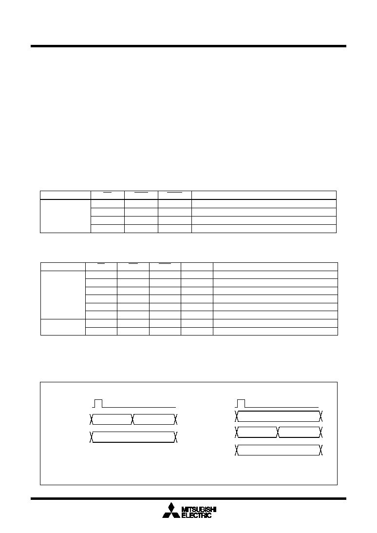
Mitsubishi microcomputers
M16C / 62A Group
SINGLE-CHIP 16-BIT CMOS MICROCOMPUTER
Bus Control
30
_____
______
________
Table 1.9.4. Operation of RD, WR, and BHE signals
Status of external data bus
RD
BHE
WR
H
L
L
L
H
L
H
L
H
L
H
H
Write 1 byte of data to odd address
Read 1 byte of data from odd address
Write 1 byte of data to even address
Read 1 byte of data from even address
Data bus width
A0
H
H
L
L
H
L
L
L
L
H
L
L
H
L
H / L
L
H
H / L
8-bit
(BYTE = "H")
Write data to both even and odd addresses
Read data from both even and odd addresses
Write 1 byte of data
Read 1 byte of data
16-bit
(BYTE = "L")
Not used
Not used
Status of external data bus
Read data
Write 1 byte of data to even address
Write 1 byte of data to odd address
Write data to both even and odd addresses
WRH
WRL
RD
Data bus width
16-bit
(BYTE = "L")
H
H
H
H
L
H
L
H
H
L
L
L
_____
________
_________
Table 1.9.3. Operation of RD, WRL, and WRH signals
(3) Read/write signals
With a 16-bit data bus (BYTE pin ="L"), bit 2 of the processor mode register 0 (address 0004
16
) select the
_____ ________
______
_____
________
_________
combinations of RD, BHE, and WR signals or RD, WRL, and WRH signals. With an 8-bit data bus (BYTE
_____
______
_______
pin = "H"), use the combination of RD, WR, and BHE signals. (Set bit 2 of the processor mode register 0
(address 0004
16
) to "0".) Tables 1.9.3 and 1.9.4 show the operation of these signals.
_____
______
________
After a reset has been cancelled, the combination of RD, WR, and BHE signals is automatically selected.
_____ _________
_________
When switching to the RD, WRL, and WRH combination, do not write to external memory until bit 2 of the
processor mode register 0 (address 0004
16
) has been set (Note).
Note: Before attempting to change the contents of the processor mode register 0, set bit 1 of the protect
register (address 000A
16
) to "1".
(4) ALE signal
The ALE signal latches the address when accessing the multiplex bus space. Latch the address when the
ALE signal falls.
When BYTE pin = "H"
When BYTE pin = "L"
ALE
Address
Data (Note 1)
Address (Note 2)
D
0
/A
0
to D
7
/A
7
A
8
to A
19
ALE
Address
Data (Note 1)
Address
D
0
/A
1
to D
7
/A
8
A
9
to A
19
Address
A
0
Note 1: Floating when reading.
Note 2: When multiplexed bus for the entire space is selected, these are I/O ports.
Figure 1.9.3. ALE signal and address/data bus

Mitsubishi microcomputers
M16C / 62A Group
SINGLE-CHIP 16-BIT CMOS MICROCOMPUTER
Bus Control
31
_____
________
Figure 1.9.4. Example of RD signal extended by RDY signal
BCLK
RD
CS
i
(i=0 to 3)
RDY
tsu(RDY - BCLK)
BCLK
RD
CS
i
(i=0 to 3)
RDY
tsu(RDY - BCLK)
In an instance of separate bus
In an instance of multiplexed bus
Accept timing of RDY signal
: Wait using RDY signal
: Wait using software
Accept timing of RDY signal
________
Note: The RDY signal cannot be received immediately prior to a software wait.
Table 1.9.5. Microcomputer status in wait state (Note)
Item
Status
Oscillation
On
___
_____
R/W signal, address bus, data bus, CS
________
Maintain status when RDY signal received
__________
ALE signal, HLDA, programmable I/O ports
Internal peripheral circuits
On
________
(5) The RDY signal
________
RDY is a signal that facilitates access to an external device that requires long access time. As shown in
________
Figure 1.9.4, if an "L" is being input to the RDY at the BCLK falling edge, the bus turns to the wait state. If
________
an "H" is being input to the RDY pin at the BCLK falling edge, the bus cancels the wait state. Table 1.9.5
shows the state of the microcomputer with the bus in the wait state, and Figure 1.9.4 shows an example
____
________
in which the RD signal is prolonged by the RDY signal.
________
The RDY signal is valid when accessing the external area during the bus cycle in which bits 4 to 7 of the
________
chip select control register (address 0008
16
) are set to "0". The RDY signal is invalid when setting "1" to
________
all bits 4 to 7 of the chip select control register (address 0008
16
), but the RDY pin should be treated as
properly as in non-using.

Mitsubishi microcomputers
M16C / 62A Group
SINGLE-CHIP 16-BIT CMOS MICROCOMPUTER
Bus Control
32
Table 1.9.6. Microcomputer status in hold state
Item
Status
Oscillation
ON
___
_____
_______
R/W signal, address bus, data bus, CS, BHE
Floating
Programmable I/O ports
P0, P1, P2, P3, P4, P5
Floating
P6, P7, P8, P9, P10
Maintains status when hold signal is received
__________
HLDA
Output "L"
Internal peripheral circuits
ON (but watchdog timer stops)
ALE signal
Undefined
__________
HOLD > DMAC > CPU
(6) Hold signal
The hold signal is used to transfer the bus privileges from the CPU to the external circuits. Inputting "L" to
__________
the HOLD pin places the microcomputer in the hold state at the end of the current bus access. This status
__________
__________
is maintained and "L" is output from the HLDA pin as long as "L" is input to the HOLD pin. Table 1.9.6
shows the microcomputer status in the hold state.
__________
Bus-using priorities are given to HOLD, DMAC, and CPU in order of decreasing precedence.
Figure 1.9.5. Bus-using priorities
(7) External bus status when the internal area is accessed
Table 1.9.7 shows the external bus status when the internal area is accessed.
Table 1.9.7. External bus status when the internal area is accessed
Item
SFR accessed
Internal ROM/RAM accessed
Address bus
Address output
Maintain status before accessed
address of external area
Data bus
When read
Floating
Floating
When write
Output data
Undefined
RD, WR, WRL, WRH
RD, WR, WRL, WRH output
Output "H"
BHE
BHE output
Maintain status before accessed
status of external area
CS
Output "H"
Output "H"
ALE
Output "L"
Output "L"

Mitsubishi microcomputers
M16C / 62A Group
SINGLE-CHIP 16-BIT CMOS MICROCOMPUTER
Bus Control
33
(9) Software wait
A software wait can be inserted by setting the wait bit (bit 7) of the processor mode register 1 (address
0005
16
) (Note) and bits 4 to 7 of the chip select control register (address 0008
16
).
A software wait is inserted in the internal ROM/RAM area and in the external memory area by setting the
wait bit of the processor mode register 1. When set to "0", each bus cycle is executed in one BCLK cycle.
When set to "1", each bus cycle is executed in two or three BCLK cycles. After the microcomputer has been
reset, this bit defaults to "0". When set to "1", a wait is applied to all memory areas (two or three BCLK
cycles), regardless of the contents of bits 4 to 7 of the chip select control register. Set this bit after referring
to the recommended operating conditions (main clock input oscillation frequency) of the electric character-
________
istics. However, when the user is using the RDY signal, the relevant bit in the chip select control register's
bits 4 to 7 must be set to "0".
When the wait bit of the processor mode register 1 is "0", software waits can be set independently for
each of the 4 areas selected using the chip select signal. Bits 4 to 7 of the chip select control register
_______
_______
correspond to chip selects CS0 to CS3. When one of these bits is set to "1", the bus cycle is executed in
one BCLK cycle. When set to "0", the bus cycle is executed in two or three BCLK cycles. These bits
default to "0" after the microcomputer has been reset.
The SFR area is always accessed in two BCLK cycles regardless of the setting of these control bits. Also,
insert a software wait if using the multiplex bus to access the external memory area.
Table 1.9.8 shows the software wait and bus cycles. Figure 1.9.6 shows example of bus timing when
using software waits.
Note: Before attempting to change the contents of the processor mode register 1, set bit 1 of the protect
register (address 000A
16
) to "1".
Area
Bus status
Wait bit
Bits 4 to 7 of chip select
control register
Bus cycle
Invalid
1
2 BCLK cycles
External
memory
area
Separate bus
0
1
1 BCLK cycle
Separate bus
0
0
2 BCLK cycles
Separate bus
1
0 (Note)
2 BCLK cycles
Multiplex bus
0
0
3 BCLK cycles
Multiplex bus
1
3 BCLK cycles
0 (Note)
SFR
Internal
ROM/RAM
0
Invalid
1 BCLK cycle
Invalid
Invalid
2 BCLK cycles
Note: When using the RDY signal, always set to "0".
Table 1.9.8. Software waits and bus cycles
(8) BCLK output
The user can choose the BCLK output by use of bit 7 of processor mode register 0 (0004
16
) (Note).
When set to "1", the output floating.
Note: Before attempting to change the contents of the processor mode register 0, set bit 1 of the protect
register (address 000A
16
) to "1".

Mitsubishi microcomputers
M16C / 62A Group
SINGLE-CHIP 16-BIT CMOS MICROCOMPUTER
Bus Control
34
Figure 1.9.6. Typical bus timings using software wait
Output
Input
Address
Address
< Separate bus (with wait) >
BCLK
Read signal
Write signal
Data bus
BCLK
Read signal
Address bus/
Data bus
Chip select (Note 2)
Address
Address
Data output
Address
Address
Input
ALE
< Multiplexed bus >
Write signal
BCLK
Read signal
Write signal
Address bus (Note 2)
Address
Address
Bus cycle (Note 1)
< Separate bus (no wait) >
Output
Data bus
Input
Note 1: These example timing charts indicate bus cycle length.
After this bus cycle sometimes come read and write cycles in succession.
Note 2: The address bus and chip select may be extended depending on the CPU status
such as that of the instruction queue buffer.
Bus cycle (Note 1)
Bus cycle (Note 1)
Bus cycle (Note 1)
Bus cycle (Note 1)
Bus cycle (Note 1)
Address bus (Note 2)
Address bus (Note 2)
Chip select (Note 2)
Chip select (Note 2)

Mitsubishi microcomputers
M16C / 62A Group
SINGLE-CHIP 16-BIT CMOS MICROCOMPUTER
Clock Generating Circuit
35
Figure 1.10.2. Examples of sub-clock
Table 1.10.1. Main clock and sub-clock generating circuits
Clock Generating Circuit
The clock generating circuit contains two oscillator circuits that supply the operating clock sources to the
CPU and internal peripheral units.
Example of oscillator circuit
Figure 1.10.1 shows some examples of the main clock circuit, one using an oscillator connected to the
circuit, and the other one using an externally derived clock for input. Figure 1.10.2 shows some examples
of sub-clock circuits, one using an oscillator connected to the circuit, and the other one using an externally
derived clock for input. Circuit constants in Figures 1.10.1 and 1.10.2 vary with each oscillator used. Use
the values recommended by the manufacturer of your oscillator.
Figure 1.10.1. Examples of main clock
Main clock generating circuit
Sub-clock generating circuit
Use of clock
∑ CPU's operating clock source
∑ CPU's operating clock source
∑ Internal peripheral units'
∑ Timer A/B's count clock
operating clock source
source
Usable oscillator
Ceramic or crystal oscillator
Crystal oscillator
Pins to connect oscillator
X
IN
, X
OUT
X
CIN
, X
COUT
Oscillation stop/restart function
Available
Available
Oscillator status immediately after reset
Oscillating
Stopped
Other
Externally derived clock can be input
Microcomputer
(Built-in feedback resistor)
X
IN
X
OUT
Externally derived clock
Open
Vcc
Vss
Microcomputer
(Built-in feedback resistor)
X
IN
X
OUT
R
d
C
IN
C
OUT
(Note)
Note: Insert a damping resistor if required. The resistance will vary depending on the oscillator and the oscillation drive
capacity setting. Use the value recommended by the maker of the oscillator.
When the oscillation drive capacity is set to low, check that oscillation is stable. Also, if the oscillator manufacturer's
data sheet specifies that a feedback resistor be added external to the chip, insert a feedback resistor between X
IN
and X
OUT
following the instruction.
Microcomputer
(Built-in feedback resistor)
X
CIN
X
COUT
Externally derived clock
Open
Vcc
Vss
Note: Insert a damping resistor if required. The resistance will vary depending on the oscillator and the oscillation drive
capacity setting. Use the value recommended by the maker of the oscillator.
When the oscillation drive capacity is set to low, check that oscillation is stable. Also, if the oscillator manufacturer's
data sheet specifies that a feedback resistor be added external to the chip, insert a feedback resistor between X
CIN
and X
COUT
following the instruction.
Microcomputer
(Built-in feedback resistor)
X
CIN
X
COUT
(Note)
C
CIN
C
COUT
R
Cd
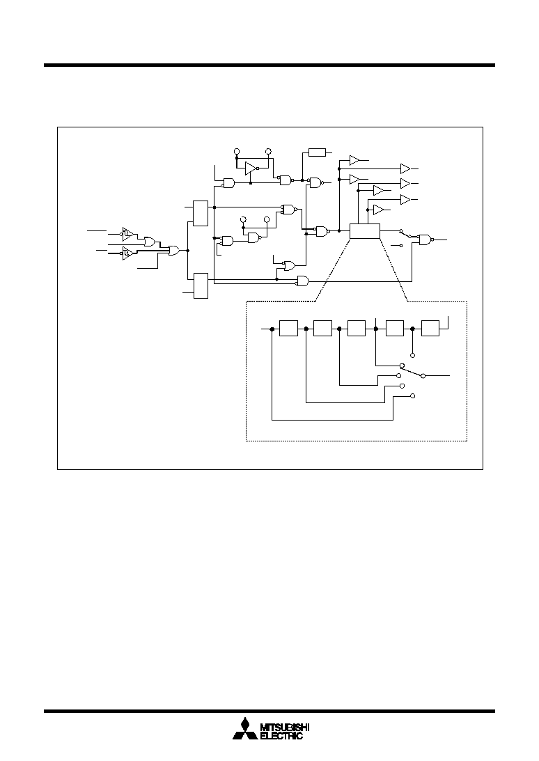
Mitsubishi microcomputers
M16C / 62A Group
SINGLE-CHIP 16-BIT CMOS MICROCOMPUTER
Clock Generating Circuit
36
Clock Control
Figure 1.10.3 shows the block diagram of the clock generating circuit.
Sub clock
CM04
f
C32
CM0i : Bit i at address 0006
16
CM1i : Bit i at address 0007
16
WDCi : Bit i at address 000F
16
X
CIN
CM10 "1"
Write signal
1/32
X
COUT
Q
S
R
WAIT instruction
X
OUT
Main clock
CM05
f
C
CM02
f
1
Q
S
R
NMI
Interrupt request
level judgment
output
RESET
Software reset
f
C
CM07=0
CM07=1
f
AD
Divider
a
d
1/2
1/2
1/2
1/2
CM06=0
CM17,CM16=00
CM06=0
CM17,CM16=01
CM06=0
CM17,CM16=10
CM06=1
CM06=0
CM17,CM16=11
d
a
Details of divider
X
IN
f
8
f
32
c
b
b
1/2
c
f
32
SIO2
f
8
SIO2
f
1
SIO2
BCLK
Figure 1.10.3. Clock generating circuit

Mitsubishi microcomputers
M16C / 62A Group
SINGLE-CHIP 16-BIT CMOS MICROCOMPUTER
Clock Generating Circuit
37
The following paragraphs describes the clocks generated by the clock generating circuit.
(1) Main clock
The main clock is generated by the main clock oscillation circuit. After a reset, the clock is divided by 8 to
the BCLK. The clock can be stopped using the main clock stop bit (bit 5 at address 0006
16
). Stopping the
clock, after switching the operating clock source of CPU to the sub-clock, reduces the power dissipation.
After the oscillation of the main clock oscillation circuit has stabilized, the drive capacity of the main clock
oscillation circuit can be reduced using the X
IN
-X
OUT
drive capacity select bit (bit 5 at address 0007
16
).
Reducing the drive capacity of the main clock oscillation circuit reduces the power dissipation. This bit
changes to "1" when shifting from high-speed/medium-speed mode to stop mode and at a reset. When
shifting from low-speed/low power dissipation mode to stop mode, the value before stop mode is re-
tained.
(2) Sub-clock
The sub-clock is generated by the sub-clock oscillation circuit. No sub-clock is generated after a reset.
After oscillation is started using the port X
C
select bit (bit 4 at address 0006
16
), the sub-clock can be
selected as the BCLK by using the system clock select bit (bit 7 at address 0006
16
). However, be sure
that the sub-clock oscillation has fully stabilized before switching.
After the oscillation of the sub-clock oscillation circuit has stabilized, the drive capacity of the sub-clock
oscillation circuit can be reduced using the X
CIN
-X
COUT
drive capacity select bit (bit 3 at address 0006
16
).
Reducing the drive capacity of the sub-clock oscillation circuit reduces the power dissipation. This bit
changes to "1" when shifting to stop mode and at a reset.
When the X
CIN
/X
COUT
is used, set ports P8
6
and P8
7
as the input ports without pull-up.
(3) BCLK
The BCLK is the clock that drives the CPU, and is f
C
or the clock is derived by dividing the main clock by
1, 2, 4, 8, or 16. The BCLK is derived by dividing the main clock by 8 after a reset. The BCLK signal can
be output from BCLK pin by the BCLK output disable bit (bit 7 at address 0004
16
) in the memory expan-
sion and the microprocessor modes.
The main clock division select bit 0(bit 6 at address 0006
16
) changes to "1" when shifting from high-
speed/medium-speed to stop mode and at reset. When shifting from low-speed/low power dissipation
mode to stop mode, the value before stop mode is retained.
(4) Peripheral function clock(f
1
, f
8
, f
32
, f
1SIO2
, f
8SIO2
,f
32SIO2
,f
AD
)
The clock for the peripheral devices is derived from the main clock or by dividing it by 1, 8, or 32. The
peripheral function clock is stopped by stopping the main clock or by setting the WAIT peripheral function
clock stop bit (bit 2 at 0006
16
) to "1" and then executing a WAIT instruction.
(5) f
C32
This clock is derived by dividing the sub-clock by 32. It is used for the timer A and timer B counts.
(6) f
C
This clock has the same frequency as the sub-clock. It is used for the BCLK and for the watchdog timer.

Mitsubishi microcomputers
M16C / 62A Group
SINGLE-CHIP 16-BIT CMOS MICROCOMPUTER
Clock Generating Circuit
38
Figure 1.10.4 shows the system clock control registers 0 and 1.
Figure 1.10.4. Clock control registers 0 and 1
System clock control register 0 (Note 1)
Symbol
Address
When reset
CM0
0006
16
48
16
Bit name
Function
Bit symbol
b7
b6
b5
b4
b3
b2
b1
b0
0 0 : I/O port P5
7
0 1 : f
C
output
1 0 : f
8
output
1 1 : f
32
output
b1 b0
CM07
CM05
CM04
CM03
CM01
CM02
CM00
CM06
Clock output function
select bit
(Valid only in single-chip
mode)
WAIT peripheral function
clock stop bit
0 : Do not stop peripheral function clock in wait mode
1 : Stop peripheral function clock in wait mode (Note 8)
X
CIN
-X
COUT
drive capacity
select bit (Note 2)
0 : LOW
1 : HIGH
Port X
C
select bit
0 : I/O port
1 : X
CIN
-X
COUT
generation (Note 9)
Main clock (X
IN
-X
OUT
)
stop bit (Note 3, 4, 5)
0 : On
1 : Off
Main clock division select
bit 0 (Note 7)
0 : CM16 and CM17 valid
1 : Division by 8 mode
System clock select bit
(Note 6)
0 : X
IN
, X
OUT
1 : X
CIN
, X
COUT
Note 1: Set bit 0 of the protect register (address 000A
16
) to "1" before writing to this register.
Note 2: Changes to "1" when shiffing to stop mode and at a reset.
Note 3: When entering low power dissipation mode, main clock stops by using this bit. To stop the main clock, when the
sub clock oscillation is stable, set system clock select bit (CM07) to "1" before setting this bit to "1".
Note 4: When inputting external clock, only clock oscillation buffer is stopped and clock input is acceptable.
Note 5: If this bit is set to "1", X
OUT
turns "H". The built-in feedback resistor remains being connected, so X
IN
turns
pulled up to X
OUT
("H") via the feedback resistor.
Note 6: Set port X
C
select bit (CM04) to "1" and stabilize the sub-clock oscillating before setting this bit from "0" to "1".
Do not write to both bits at the same time. And also, set the main clock stop bit (CM05) to "0" and stabilize the
main clock oscillating before setting this bit from "1" to "0".
Note 7: This bit changes to "1" when shifting from high-speed/medium-speed mode to stop mode and at a reset. When
shifting from low-speed/low power dissipation mode to stop mode, the value before stop mode is retained.
Note 8: f
C32
is not included.
Do not set to
"1"
when using low-speed or low power dissipation mode.
Note 9: When the X
CIN
/X
COUT
is used, set ports P8
6
and P8
7
as the input ports without pull-up.
System clock control register 1 (Note 1)
Symbol
Address
When reset
CM1
0007
16
20
16
Bit name
Function
Bit symbol
b7
b6
b5
b4
b3
b2
b1
b0
CM10
All clock stop control bit
(Note4)
0 : Clock on
1 : All clocks off (stop mode)
Note 1: Set bit 0 of the protect register (address 000A
16
) to
"1" before writing to this register.
Note 2: This bit changes to "1" when shifting from high-speed/medium-speed mode to stop mode and at a reset. When
shifting from low-speed/low power dissipation mode to stop mode, the value before stop mode is retained.
Note 3: Can be selected when bit 6 of the system clock control register 0 (address 0006
16
) is
"0". If
"1", division mode is
fixed at 8.
Note 4: If this bit is set to "1", X
OUT
turns "H", and the built-in feedback resistor is cut off. X
CIN
and X
COUT
turn high-
impedance state.
CM15
X
IN
-X
OUT
drive capacity
select bit (Note 2)
0 : LOW
1 : HIGH
W
R
W
R
CM16
CM17
Reserved bit
Always set to
"0"
Reserved bit
Always set to
"0"
Main clock division
select bit 1 (Note 3)
0 0 : No division mode
0 1 : Division by 2 mode
1 0 : Division by 4 mode
1 1 : Division by 16 mode
b7 b6
0
0
Reserved bit
Always set to
"0"
Reserved bit
Always set to
"0"
0
0

Mitsubishi microcomputers
M16C / 62A Group
SINGLE-CHIP 16-BIT CMOS MICROCOMPUTER
Clock Generating Circuit
39
Pin
Memory expansion mode
Single-chip mode
Microprocessor mode
_______
_______
Address bus, data bus, CS0 to CS3,
Retains status before stop mode
________
BHE
_____
______
________
_________
RD, WR, WRL, WRH
"H"
__________
HLDA, BCLK
"H"
ALE
"H"
Port
Retains status before stop mode Retains status before stop mode
CLK
OUT
When fc selected
Valid only in single-chip mode
"H"
When f
8
, f
32
selected
Valid only in single-chip mode
Retains status before stop mode
Table 1.10.2. Port status during stop mode
Clock Output
In single-chip mode, the clock output function select bits (bits 0 and 1 at address 0006
16
) enable f
8
, f
32
, or
fc to be output from the P5
7
/CLK
OUT
pin. When the WAIT peripheral function clock stop bit (bit 2 at address
0006
16
) is set to "1", the output of f
8
and f
32
stops when a WAIT instruction is executed.
Stop Mode
Writing "1" to the all-clock stop control bit (bit 0 at address 0007
16
) stops all oscillation and the microcom-
puter enters stop mode. In stop mode, the content of the internal RAM is retained provided that V
CC
re-
mains above 2V.
Because the oscillation , BCLK, f
1
to f
32
, f
1SIO2
to f
32SIO2
, f
C
, f
C32
, and f
AD
stops in stop mode, peripheral
functions such as the A-D converter and watchdog timer do not function. However, timer A and timer B
operate provided that the event counter mode is set to an external pulse, and UARTi(i = 0 to 2), SI/O3,4
functions provided an external clock is selected. Table 1.10.2 shows the status of the ports in stop mode.
Stop mode is cancelled by a hardware reset or an interrupt. If an interrupt is to be used to cancel stop mode,
that interrupt must first have been enabled, and the priority level of the interrupt which is not used to cancel
must have been changed to 0. If returning by an interrupt, that interrupt routine is executed. If only a
_______
hardware reset or an NMI interrupt is used to cancel stop mode, change the priority level of all interrupt to
0, then shift to stop mode.
When shifting from high-speed/medium-speed mode to stop mode and at a reset, the main clock division
select bit 0 (bit 6 at address 0006
16
) is set to "1". When shifting from low-speed/low power dissipation mode
to stop mode, the value before stop mode is retained.

Mitsubishi microcomputers
M16C / 62A Group
SINGLE-CHIP 16-BIT CMOS MICROCOMPUTER
Wait Mode
40
Table 1.10.3. Port status during wait mode
Pin
Memory expansion mode
Single-chip mode
Microprocessor mode
_______
_______
Address bus, data bus, CS0 to CS3,
Retains status before wait mode
________
BHE
_____
______
________
_________
RD, WR, WRL, WRH
"H"
__________
HLDA,BCLK
"H"
ALE
"H"
Port
Retains status before wait mode
Retains status before wait mode
CLK
OUT
When f
C
selected
Valid only in single-chip mode
Does not stop
When f
8
, f
32
selected Valid only in single-chip mode
Does not stop when the WAIT
peripheral function clock stop
bit is "0".
When the WAIT peripheral
function clock stop bit is "1",
the status immediately prior
to entering wait mode is main-
tained.
Wait Mode
When a WAIT instruction is executed, the BCLK stops and the microcomputer enters the wait mode. In this
mode, oscillation continues but the BCLK and watchdog timer stop. Writing "1" to the WAIT peripheral
function clock stop bit and executing a WAIT instruction stops the clock being supplied to the internal
peripheral functions, allowing power dissipation to be reduced. However, peripheral function clock f
C32
does not stop so that the peripherals using f
C32
do not contribute to the power saving. When the MCU
running in low-speed or low power dissipation mode, do not enter WAIT mode with this bit set to "1". Table
1.10.3 shows the status of the ports in wait mode.
Wait mode is cancelled by a hardware reset or an interrupt. If an interrupt is used to cancel wait mode, that
interrupt must first have been enabled, and the priority level of the interrupt which is not used to cancel must
have been changed to 0. If returning by an interrupt, the clock in which the WAIT instruction executed is set
to BCLK by the microcomputer, and the action is resumed from the interrupt routine. If only a hardware
_______
reset or an NMI interrupt is used to cancel wait mode, change the priority level of all interrupt to 0,then shift
to wait mode.

Mitsubishi microcomputers
M16C / 62A Group
SINGLE-CHIP 16-BIT CMOS MICROCOMPUTER
Status Transition of BCLK
41
0
1
0
0
0
Invalid
Division by 2 mode
1
0
0
0
0
Invalid
Division by 4 mode
Invalid
Invalid
0
1
0
Invalid
Division by 8 mode
1
1
0
0
0
Invalid
Division by 16 mode
0
0
0
0
0
Invalid
No-division mode
Invalid
Invalid
1
Invalid
0
1
Low-speed mode
Invalid
Invalid
1
Invalid
1
1
Low power dissipation mode
Status Transition of BCLK
Power dissipation can be reduced and low-voltage operation achieved by changing the count source for
BCLK. Table 1.10.4 shows the operating modes corresponding to the settings of system clock control
registers 0 and 1.
When reset, the device starts in division by 8 mode. The main clock division select bit 0(bit 6 at address
0006
16
) changes to "1" when shifting from high-speed/medium-speed to stop mode and at a reset. When
shifting from low-speed/low power dissipation mode to stop mode, the value before stop mode is retained.
The following shows the operational modes of BCLK.
(1) Division by 2 mode
The main clock is divided by 2 to obtain the BCLK.
(2) Division by 4 mode
The main clock is divided by 4 to obtain the BCLK.
(3) Division by 8 mode
The main clock is divided by 8 to obtain the BCLK. When reset, the device starts operating from this
mode. Before the user can go from this mode to no division mode, division by 2 mode, or division by 4
mode, the main clock must be oscillating stably. When going to low-speed or lower power consumption
mode, make sure the sub-clock is oscillating stably.
(4) Division by 16 mode
The main clock is divided by 16 to obtain the BCLK.
(5) No-division mode
The main clock is divided by 1 to obtain the BCLK.
(6) Low-speed mode
f
C
is used as the BCLK. Note that oscillation of both the main and sub-clocks must have stabilized before
transferring from this mode to another or vice versa. At least 2 to 3 seconds are required after the sub-
clock starts. Therefore, the program must be written to wait until this clock has stabilized immediately
after powering up and after stop mode is cancelled.
(7) Low power dissipation mode
f
C
is the BCLK and the main clock is stopped.
Note : Before the count source for BCLK can be changed from X
IN
to X
CIN
or vice versa, the clock to which
the count source is going to be switched must be oscillating stably. Allow a wait time in software for
the oscillation to stabilize before switching over the clock.
CM17
CM16
CM07
CM06
CM05
CM04
Operating mode of BCLK
Table 1.10.4. Operating modes dictated by settings of system clock control registers 0 and 1

Mitsubishi microcomputers
M16C / 62A Group
SINGLE-CHIP 16-BIT CMOS MICROCOMPUTER
Power control
42
Power control
The following is a description of the three available power control modes:
Modes
Power control is available in three modes.
(a) Normal operation mode
∑ High-speed mode
Divide-by-1 frequency of the main clock becomes the BCLK. The CPU operates with the BCLK.
Each peripheral function operates according to its assigned clock.
∑ Medium-speed mode
Divide-by-2, divide-by-4, divide-by-8, or divide-by-16 frequency of the main clock becomes the
BCLK. The CPU operates with the BCLK. Each peripheral function operates according to its as-
signed clock.
∑ Low-speed mode
f
C
becomes the BCLK. The CPU operates according to the f
C
clock. The f
C
clock is supplied by the
subclock. Each peripheral function operates according to its assigned clock.
∑ Low power dissipation mode
The main clock operating in low-speed mode is stopped. The CPU operates according to the f
C
clock. The f
C
clock is supplied by the subclock. The only peripheral functions that operate are those
with the subclock selected as the count source.
(b) Wait mode
The CPU operation is stopped. The oscillators do not stop.
(c) Stop mode
All oscillators stop. The CPU and all built-in peripheral functions stop. This mode, among the three
modes listed here, is the most effective in decreasing power consumption.
Figure 1.10.5 is the state transition diagram of the above modes.

Mitsubishi microcomputers
M16C / 62A Group
SINGLE-CHIP 16-BIT CMOS MICROCOMPUTER
Power control
43
Figure 1.10.5. State transition diagram of Power control mode
Transition of stop mode, wait mode
Transition of normal mode
Reset
Medium-speed mode
(divided-by-8 mode)
Interrupt
CM10 = "1"
All oscillators stopped
CPU operation stopped
Medium-speed mode
(divided-by-8 mode)
BCLK : f(X
IN
)/8
CM07 = "0" CM06 = "1"
Low-speed mode
High-speed mode
Main clock is oscillating
Sub clock is stopped
Main clock is oscillating
Sub clock is stopped
Main clock is stopped
Sub clock is oscillating
Main clock is oscillating
Sub clock is oscillating
Low power dissipation mode
High-speed/medium-
speed mode
Low-speed/low power
dissipation mode
Normal mode
Stop mode
Stop mode
Stop mode
All oscillators stopped
All oscillators stopped
Wait mode
Wait mode
Wait mode
CPU operation stopped
CPU operation stopped
Interrupt
WAIT
instruction
Interrupt
WAIT
instruction
Interrupt
WAIT
instruction
CM10 = "1"
Interrupt
Interrupt
CM10 = "1"
BCLK : f(X
IN
)/2
CM07 = "0" CM06 = "0"
CM17 = "0" CM16 = "1"
Medium-speed mode
(divided-by-2 mode)
BCLK : f(X
IN
)/16
CM07 = "0" CM06 = "0"
CM17 = "1" CM16 = "1"
Medium-speed mode
(divided-by-16 mode)
BCLK : f(X
IN
)/4
CM07 = "0" CM06 = "0"
CM17 = "1" CM16 = "0"
Medium-speed mode
(divided-by-4 mode)
BCLK : f(X
IN
)
CM07 = "0" CM06 = "0"
CM17 = "0" CM16 = "0"
BCLK : f(X
IN
)/8
Medium-speed mode
(divided-by-8 mode)
CM07 = "0"
CM06 = "1"
High-speed mode
BCLK : f(X
IN
)/2
CM07 = "0" CM06 = "0"
CM17 = "0" CM16 = "1"
Medium-speed mode
(divided-by-2 mode)
BCLK : f(X
IN
)/16
CM07 = "0" CM06 = "0"
CM17 = "1" CM16 = "1"
Medium-speed mode
(divided-by-16 mode)
BCLK : f(X
IN
)/4
CM07 = "0" CM06 = "0"
CM17 = "1" CM16 = "0"
Medium-speed mode
(divided-by-4 mode)
BCLK : f(X
IN
)
CM07 = "0" CM06 = "0"
CM17 = "0" CM16 = "0"
BCLK : f(X
CIN
)
CM07 = "1"
BCLK : f(X
CIN
)
CM07 = "1"
Main clock is oscillating
Sub clock is oscillating
CM07 = "0"
(Note 1, 3)
CM07 = "0" (Note 1)
CM06 = "1"
CM04 = "0"
CM07 = "1"
(Note 2)
CM07 = "0" (Note 1)
CM06 = "0" (Note 3)
CM04 = "1"
CM07 = "1" (Note 2)
CM05 = "1"
CM05 = "0"
CM05 = "1"
CM04 = "0"
CM04 = "1"
CM06 = "0"
(Notes 1,3)
CM06 = "1"
CM04 = "0"
CM04 = "1"
(Notes 1, 3)
Note 1: Switch clock after oscillation of main clock is sufficiently stable.
Note 2: Switch clock after oscillation of sub clock is sufficiently stable.
Note 3: Change CM06 after changing CM17 and CM16.
Note 4: Transit in accordance with arrow.
(Refer to the following for the transition of normal mode.)

Mitsubishi microcomputers
M16C / 62A Group
SINGLE-CHIP 16-BIT CMOS MICROCOMPUTER
Protection
44
Protection
The protection function is provided so that the values in important registers cannot be changed in the event
that the program runs out of control. Figure 1.10.6 shows the protect register. The values in the processor
mode register 0 (address 0004
16
), processor mode register 1 (address 0005
16
), system clock control reg-
ister 0 (address 0006
16
), system clock control register 1 (address 0007
16
), port P9 direction register (ad-
dress 03F3
16
) , SI/O3 control register (address 0362
16
) and SI/O4 control register (address 0366
16
) can
only be changed when the respective bit in the protect register is set to "1". Therefore, important outputs
can be allocated to port P9.
If, after "1" (write-enabled) has been written to the port P9 direction register and SI/Oi control register
(i=3,4) write-enable bit (bit 2 at address 000A
16
), a value is written to any address, the bit automatically
reverts to "0" (write-inhibited). However, the system clock control registers 0 and 1 write-enable bit (bit 0 at
000A
16
) and processor mode register 0 and 1 write-enable bit (bit 1 at 000A
16
) do not automatically return
to "0" after a value has been written to an address. The program must therefore be written to return these
bits to "0".
Protect register
Symbol
Address
When reset
PRCR
000A
16
XXXXX000
2
Bit name
Bit symbol
b7
b6
b5
b4
b3
b2
b1
b0
0 : Write-inhibited
1 : Write-enabled
PRC1
PRC0
PRC2
Enables writing to processor mode
registers 0 and 1 (addresses 0004
16
and 0005
16
)
Function
0 : Write-inhibited
1 : Write-enabled
Enables writing to system clock
control registers 0 and 1 (addresses
0006
16
and 0007
16
)
Enables writing to port P9 direction
register (address 03F3
16
) and SI/Oi
control register (i=3,4) (addresses
0362
16
and 0366
16
) (Note
)
0 : Write-inhibited
1 : Write-enabled
W
R
Nothing is assigned.
In an attempt to write to these bits, write "0". The value, if read, turns out to be
indeterminate.
Note: Writing a value to an address after "1" is written to this bit returns the bit
to "0" . Other bits do not automatically return to "0" and they must therefore
be reset by the program.
Figure 1.10.6. Protect register

Mitsubishi microcomputers
M16C / 62A Group
SINGLE-CHIP 16-BIT CMOS MICROCOMPUTER
Interrupt
45
∑ Maskable interrupt :
An interrupt which can be enabled (disabled) by the interrupt enable flag
(I flag) or whose interrupt priority can be changed by priority level.
∑ Non-maskable interrupt : An interrupt which cannot be enabled (disabled) by the interrupt enable flag
(I flag) or whose interrupt priority cannot be changed by priority level.
Figure 1.11.1. Classification of interrupts
Interrupt
Software
Hardware
Special
Peripheral I/O (Note)
Undefined instruction (UND instruction)
Overflow (INTO instruction)
BRK instruction
INT instruction
Reset
_______
NMI
________
DBC
Watchdog timer
Single step
Address matched
Note: Peripheral I/O interrupts are generated by the peripheral functions built into the microcomputer system.
Overview of Interrupt
Type of Interrupts
Figure 1.11.1 lists the types of interrupts.

Mitsubishi microcomputers
M16C / 62A Group
SINGLE-CHIP 16-BIT CMOS MICROCOMPUTER
Interrupt
46
Software Interrupts
A software interrupt occurs when executing certain instructions. Software interrupts are non-maskable
interrupts.
∑ Undefined instruction interrupt
An undefined instruction interrupt occurs when executing the UND instruction.
∑ Overflow interrupt
An overflow interrupt occurs when executing the INTO instruction with the overflow flag (O flag) set to
"1". The following are instructions whose O flag changes by arithmetic:
ABS, ADC, ADCF, ADD, CMP, DIV, DIVU, DIVX, NEG, RMPA, SBB, SHA, SUB
∑ BRK interrupt
A BRK interrupt occurs when executing the BRK instruction.
∑ INT interrupt
An INT interrupt occurs when specifying one of software interrupt numbers 0 through 63 and execut-
ing the INT instruction. Software interrupt numbers 0 through 31 are assigned to peripheral I/O inter-
rupts, so executing the INT instruction allows executing the same interrupt routine that a peripheral I/
O interrupt does.
The stack pointer (SP) used for the INT interrupt is dependent on which software interrupt number is
involved.
So far as software interrupt numbers 0 through 31 are concerned, the microcomputer saves the stack
pointer assignment flag (U flag) when it accepts an interrupt request. If change the U flag to "0" and
select the interrupt stack pointer (ISP), and then execute an interrupt sequence. When returning from
the interrupt routine, the U flag is returned to the state it was before the acceptance of interrupt re-
quest. So far as software numbers 32 through 63 are concerned, the stack pointer does not make a
shift.

Mitsubishi microcomputers
M16C / 62A Group
SINGLE-CHIP 16-BIT CMOS MICROCOMPUTER
Interrupt
47
Hardware Interrupts
Hardware interrupts are classified into two types -- special interrupts and peripheral I/O interrupts.
(1) Special interrupts
Special interrupts are non-maskable interrupts.
∑ Reset
____________
Reset occurs if an "L" is input to the RESET pin.
_______
∑ NMI interrupt
_______
_______
An NMI interrupt occurs if an "L" is input to the NMI pin.
________
∑ DBC interrupt
This interrupt is exclusively for the debugger, do not use it in other circumstances.
∑ Watchdog timer interrupt
Generated by the watchdog timer.
∑ Single-step interrupt
This interrupt is exclusively for the debugger, do not use it in other circumstances. With the debug
flag (D flag) set to "1", a single-step interrupt occurs after one instruction is executed.
∑ Address match interrupt
An address match interrupt occurs immediately before the instruction held in the address indicated by
the address match interrupt register is executed with the address match interrupt enable bit set to "1".
If an address other than the first address of the instruction in the address match interrupt register is set,
no address match interrupt occurs.
(2) Peripheral I/O interrupts
A peripheral I/O interrupt is generated by one of built-in peripheral functions. Built-in peripheral func-
tions are dependent on classes of products, so the interrupt factors too are dependent on classes of
products. The interrupt vector table is the same as the one for software interrupt numbers 0 through
31 the INT instruction uses. Peripheral I/O interrupts are maskable interrupts.
∑ Bus collision detection interrupt
This is an interrupt that the serial I/O bus collision detection generates.
∑ DMA0 interrupt, DMA1 interrupt
These are interrupts that DMA generates.
∑ Key-input interrupt
___
A key-input interrupt occurs if an "L" is input to the KI pin.
∑ A-D conversion interrupt
This is an interrupt that the A-D converter generates.
∑ UART0, UART1, UART2/NACK, SI/O3 and SI/O4 transmission interrupt
These are interrupts that the serial I/O transmission generates.
∑ UART0, UART1, UART2/ACK, SI/O3 and SI/O4 reception interrupt
These are interrupts that the serial I/O reception generates.
∑ Timer A0 interrupt through timer A4 interrupt
These are interrupts that timer A generates
∑ Timer B0 interrupt through timer B5 interrupt
These are interrupts that timer B generates.
________
________
∑ INT0 interrupt through INT5 interrupt
______
______
An INT interrupt occurs if either a rising edge or a falling edge or a both edge is input to the INT pin.

Mitsubishi microcomputers
M16C / 62A Group
SINGLE-CHIP 16-BIT CMOS MICROCOMPUTER
Interrupt
48
Interrupt source
Vector table addresses
Remarks
Address (L) to address (H)
Undefined instruction
FFFDC
16
to FFFDF
16
Interrupt on UND instruction
Overflow
FFFE0
16
to FFFE3
16
Interrupt on INTO instruction
BRK instruction
FFFE4
16
to FFFE7
16
If the vector contains FF
16
, program execution starts from
the address shown by the vector in the variable vector table
Address match
FFFE8
16
to FFFEB
16
There is an address-matching interrupt enable bit
Single step (Note)
FFFEC
16
to FFFEF
16
Do not use
Watchdog timer
FFFF0
16
to FFFF3
16
________
DBC (Note)
FFFF4
16
to FFFF7
16
Do not use
_______
NMI
FFFF8
16
to FFFFB
16
_______
External interrupt by input to NMI pin
Reset
FFFFC
16
to FFFFF
16
Note: Interrupts used for debugging purposes only.
Figure 1.11.2. Format for specifying interrupt vector addresses
Mid address
Low address
0 0 0 0
High address
0 0 0 0
0 0 0 0
Vector address + 0
Vector address + 1
Vector address + 2
Vector address + 3
LSB
MSB
Interrupts and Interrupt Vector Tables
If an interrupt request is accepted, a program branches to the interrupt routine set in the interrupt vector
table. Set the first address of the interrupt routine in each vector table. Figure 1.11.2 shows the format for
specifying the address.
Two types of interrupt vector tables are available -- fixed vector table in which addresses are fixed and
variable vector table in which addresses can be varied by the setting.
∑ Fixed vector tables
The fixed vector table is a table in which addresses are fixed. The vector tables are located in an area
extending from FFFDC
16
to FFFFF
16
. One vector table comprises four bytes. Set the first address of
interrupt routine in each vector table. Table 1.11.1 shows the interrupts assigned to the fixed vector
tables and addresses of vector tables.
Table 1.11.1. Interrupts assigned to the fixed vector tables and addresses of vector tables

Mitsubishi microcomputers
M16C / 62A Group
SINGLE-CHIP 16-BIT CMOS MICROCOMPUTER
Interrupt
49
Table 1.11.2. Interrupts assigned to the variable vector tables and addresses of vector tables
Software interrupt number
Interrupt source
Vector table address
Address (L) to address (H)
Remarks
Cannot be masked I flag
+0 to +3 (Note 1)
BRK instruction
Software interrupt number 0
+44 to +47 (Note 1)
Software interrupt number 11
+48 to +51 (Note 1)
Software interrupt number 12
+52 to +55 (Note 1)
Software interrupt number 13
+56 to +59 (Note 1)
Software interrupt number 14
+68 to +71 (Note 1)
Software interrupt number 17
+72 to +75 (Note 1)
Software interrupt number 18
+76 to +79 (Note 1)
Software interrupt number 19
+80 to +83 (Note 1)
Software interrupt number 20
+84 to +87 (Note 1)
Software interrupt number 21
+88 to +91 (Note 1)
Software interrupt number 22
+92 to +95 (Note 1)
Software interrupt number 23
+96 to +99 (Note 1)
Software interrupt number 24
+100 to +103 (Note 1)
Software interrupt number 25
+104 to +107 (Note 1)
Software interrupt number 26
+108 to +111 (Note 1)
Software interrupt number 27
+112 to +115 (Note 1)
Software interrupt number 28
+116 to +119 (Note 1)
Software interrupt number 29
+120 to +123 (Note 1)
Software interrupt number 30
+124 to +127 (Note 1)
Software interrupt number 31
+128 to +131 (Note 1)
Software interrupt number 32
+252 to +255 (Note 1)
Software interrupt number 63
to
Note 1: Address relative to address in interrupt table register (INTB).
Note 2: It is selected by interrupt request cause bit (bit 6, 7 in address 035F
16
).
Note 3: When IIC mode is selected, NACK and ACK interrupts are selected.
Cannot be masked I flag
+40 to +43 (Note 1)
Software interrupt number 10
+60 to +63 (Note 1)
Software interrupt number 15
+64 to +67 (Note 1)
Software interrupt number 16
+20 to +23 (Note 1)
Software interrupt number 5
+24 to +27 (Note 1)
Software interrupt number 6
+28 to +31 (Note 1)
Software interrupt number 7
+32 to +35 (Note 1)
Software interrupt number 8
+16 to +19 (Note 1)
INT3
Software interrupt number 4
+36 to +39 (Note 1)
SI/O3/INT4
Software interrupt number 9
SI/O4/INT5
Timer B3
Timer B4
Timer B5
(Note 2)
(Note 2)
to
DMA0
DMA1
Key input interrupt
A-D
UART0 transmit
UART0 receive
UART1 transmit
UART1 receive
Timer A0
Timer A1
Timer A2
Timer A3
Timer A4
Timer B0
Timer B1
Timer B2
INT0
INT1
INT2
Software interrupt
Bus collision detection
UART2 transmit/NACK (Note 3)
UART2 receive/ACK (Note 3)
∑ Variable vector tables
The addresses in the variable vector table can be modified, according to the user's settings. Indicate
the first address using the interrupt table register (INTB). The 256-byte area subsequent to the ad-
dress the INTB indicates becomes the area for the variable vector tables. One vector table comprises
four bytes. Set the first address of the interrupt routine in each vector table. Table 1.11.2 shows the
interrupts assigned to the variable vector tables and addresses of vector tables.

Mitsubishi microcomputers
M16C / 62A Group
SINGLE-CHIP 16-BIT CMOS MICROCOMPUTER
Interrupt
50
Interrupt Control
Descriptions are given here regarding how to enable or disable maskable interrupts and how to set the
priority to be accepted. What is described here does not apply to non-maskable interrupts.
Enable or disable a maskable interrupt using the interrupt enable flag (I flag), interrupt priority level selec-
tion bit, or processor interrupt priority level (IPL). Whether an interrupt request is present or absent is
indicated by the interrupt request bit. The interrupt request bit and the interrupt priority level selection bit
are located in the interrupt control register of each interrupt. Also, the interrupt enable flag (I flag) and the
IPL are located in the flag register (FLG).
Figure 1.11.3 shows the memory map of the interrupt control registers.

Mitsubishi microcomputers
M16C / 62A Group
SINGLE-CHIP 16-BIT CMOS MICROCOMPUTER
Interrupt
51
Figure 1.11.3. Interrupt control registers
Symbol
Address
When reset
INTiIC(i=3)
0044
16
XX00X000
2
SiIC/INTjIC (i=4, 3)
0048
16
, 0049
16
XX00X000
2
(j=5, 4)
0048
16
, 0049
16
XX00X000
2
INTiIC(i=0 to 2)
005D
16
to 005F
16
XX00X000
2
Bit name
Function
Bit symbol
W
R
b7
b6
b5
b4
b3
b2
b1
b0
ILVL0
IR
POL
Nothing is assigned.
In an attempt to write to these bits, write "0". The value, if read, turns
out to be indeterminate.
Interrupt priority level
select bit
Interrupt request bit
Polarity select bit
Reserved bit
0: Interrupt not requested
1: Interrupt requested
0 : Selects falling edge
1 : Selects rising edge
Always set to "0"
ILVL1
ILVL2
Note 1: This bit can only be accessed for reset (= 0), but cannot be accessed for set (= 1).
Note 2: To rewrite the interrupt control register, do so at a point that does not generate the
interrupt request for that register. For details, see the precautions for interrupts.
(Note 1)
Interrupt control register (Note2)
b7
b6
b5
b4
b3
b2
b1
b0
Bit name
Function
Bit symbol
W
R
Symbol
Address
When reset
TBiIC(i=3 to 5)
0045
16
to 0047
16
XXXXX000
2
BCNIC
004A
16
XXXXX000
2
DMiIC(i=0, 1)
004B
16
, 004C
16
XXXXX000
2
KUPIC
004D
16
XXXXX000
2
ADIC
004E
16
XXXXX000
2
SiTIC(i=0 to 2)
0051
16
, 0053
16
, 004F
16
XXXXX000
2
SiRIC(i=0 to 2)
0052
16
, 0054
16
, 0050
16
XXXXX000
2
TAiIC(i=0 to 4)
0055
16
to 0059
16
XXXXX000
2
TBiIC(i=0 to 2)
005A
16
to 005C
16
XXXXX000
2
ILVL0
IR
Interrupt priority level
select bit
Interrupt request bit
0 : Interrupt not requested
1 : Interrupt requested
ILVL1
ILVL2
Nothing is assigned.
In an attempt to write to these bits, write "0". The value, if read, turns
out to be indeterminate.
(Note 1)
Note 1: This bit can only be accessed for reset (= 0), but cannot be accessed for set (= 1).
Note 2: To rewrite the interrupt control register, do so at a point that does not generate the
interrupt request for that register. For details, see the precautions for interrupts.
0 0 0 : Level 0 (interrupt disabled)
0 0 1 : Level 1
0 1 0 : Level 2
0 1 1 : Level 3
1 0 0 : Level 4
1 0 1 : Level 5
1 1 0 : Level 6
1 1 1 : Level 7
b2 b1 b0
0 0 0 : Level 0 (interrupt disabled)
0 0 1 : Level 1
0 1 0 : Level 2
0 1 1 : Level 3
1 0 0 : Level 4
1 0 1 : Level 5
1 1 0 : Level 6
1 1 1 : Level 7
b2 b1 b0
0

Mitsubishi microcomputers
M16C / 62A Group
SINGLE-CHIP 16-BIT CMOS MICROCOMPUTER
Interrupt
52
Interrupt Enable Flag (I flag)
The interrupt enable flag (I flag) controls the enabling and disabling of maskable interrupts. Setting this
flag to "1" enables all maskable interrupts; setting it to "0" disables all maskable interrupts. This flag is set
to "0" after reset.
Interrupt Request Bit
The interrupt request bit is set to "1" by hardware when an interrupt is requested. After the interrupt is
accepted and jumps to the corresponding interrupt vector, the request bit is set to "0" by hardware. The
interrupt request bit can also be set to "0" by software. (Do not set this bit to "1").
Table 1.11.4. Interrupt levels enabled according
to the contents of the IPL
Table 1.11.3. Settings of interrupt priority
levels
Interrupt priority
level select bit
Interrupt priority
level
Priority
order
0 0 0
0 0 1
0 1 0
0 1 1
1 0 0
1 0 1
1 1 0
1 1 1
Level 0 (interrupt disabled)
Level 1
Level 2
Level 3
Level 4
Level 5
Level 6
Level 7
Low
High
b2 b1 b0
Enabled interrupt priority levels
0 0 0
0 0 1
0 1 0
0 1 1
1 0 0
1 0 1
1 1 0
1 1 1
Interrupt levels 1 and above are enabled
Interrupt levels 2 and above are enabled
Interrupt levels 3 and above are enabled
Interrupt levels 4 and above are enabled
Interrupt levels 5 and above are enabled
Interrupt levels 6 and above are enabled
Interrupt levels 7 and above are enabled
All maskable interrupts are disabled
IPL
2
IPL
1
IPL
0
IPL
Interrupt Priority Level Select Bit and Processor Interrupt Priority Level (IPL)
Set the interrupt priority level using the interrupt priority level select bit, which is one of the component bits
of the interrupt control register. When an interrupt request occurs, the interrupt priority level is compared
with the IPL. The interrupt is enabled only when the priority level of the interrupt is higher than the IPL.
Therefore, setting the interrupt priority level to "0" disables the interrupt.
Table 1.11.3 shows the settings of interrupt priority levels and Table 1.11.4 shows the interrupt levels
enabled, according to the contents of the IPL.
The following are conditions under which an interrupt is accepted:
∑ interrupt enable flag (I flag) = "1"
∑ interrupt request bit = "1"
∑ interrupt priority level > IPL
The interrupt enable flag (I flag), the interrupt request bit, the interrupt priority select bit, and the IPL are
independent, and they are not affected by one another.

Mitsubishi microcomputers
M16C / 62A Group
SINGLE-CHIP 16-BIT CMOS MICROCOMPUTER
Interrupt
53
Example 1:
INT_SWITCH1:
FCLR
I
; Disable interrupts.
AND.B
#00h, 0055h
; Clear TA0IC int. priority level and int. request bit.
NOP
; Four NOP instructions are required when using HOLD function.
NOP
FSET
I
; Enable interrupts.
Example 2:
INT_SWITCH2:
FCLR
I
; Disable interrupts.
AND.B
#00h, 0055h
; Clear TA0IC int. priority level and int. request bit.
MOV.W MEM, R0
; Dummy read.
FSET
I
; Enable interrupts.
Example 3:
INT_SWITCH3:
PUSHC FLG
; Push Flag register onto stack
FCLR
I
; Disable interrupts.
AND.B
#00h, 0055h
; Clear TA0IC int. priority level and int. request bit.
POPC
FLG
; Enable interrupts.
The reason why two NOP instructions (four when using the HOLD function) or dummy read are inserted
before FSET I in Examples 1 and 2 is to prevent the interrupt enable flag I from being set before the
interrupt control register is rewritten due to effects of the instruction queue.
Rewrite the interrupt control register
To rewrite the interrupt control register, do so at a point that does not generate the interrupt request for
that register. If there is possibility of the interrupt request occur, rewrite the interrupt control register after
the interrupt is disabled. The program examples are described as follow:
When a instruction to rewrite the interrupt control register is executed but the interrupt is disabled, the
interrupt request bit is not set sometimes even if the interrupt request for that register has been gener-
ated. This will depend on the instruction. If this creates problems, use the below instructions to change
the register.
Instructions : AND, OR, BCLR, BSET

Mitsubishi microcomputers
M16C / 62A Group
SINGLE-CHIP 16-BIT CMOS MICROCOMPUTER
Interrupt
54
Interrupt Sequence
An interrupt sequence -- what are performed over a period from the instant an interrupt is accepted to the
instant the interrupt routine is executed -- is described here.
If an interrupt occurs during execution of an instruction, the processor determines its priority when the
execution of the instruction is completed, and transfers control to the interrupt sequence from the next
cycle. If an interrupt occurs during execution of either the SMOVB, SMOVF, SSTR or RMPA instruction,
the processor temporarily suspends the instruction being executed, and transfers control to the interrupt
sequence.
In the interrupt sequence, the processor carries out the following in sequence given:
(1) CPU gets the interrupt information (the interrupt number and interrupt request level) by reading ad-
dress 00000
16
. After this, the corresponding interrupt request bit becomes "0".
(2) Saves the content of the flag register (FLG) as it was immediately before the start of interrupt sequence
in the temporary register (Note) within the CPU.
(3) Sets the interrupt enable flag (I flag), the debug flag (D flag), and the stack pointer select flag (U flag) to
"0" (the U flag, however does not change if the INT instruction, in software interrupt numbers 32
through 63, is executed)
(4) Saves the content of the temporary register (Note) within the CPU in the stack area.
(5) Saves the content of the program counter (PC) in the stack area.
(6) Sets the interrupt priority level of the accepted instruction in the IPL.
After the interrupt sequence is completed, the processor resumes executing instructions from the first
address of the interrupt routine.
Note: This register cannot be utilized by the user.
Interrupt Response Time
'Interrupt response time' is the period between the instant an interrupt occurs and the instant the first
instruction within the interrupt routine has been executed. This time comprises the period from the
occurrence of an interrupt to the completion of the instruction under execution at that moment (a) and the
time required for executing the interrupt sequence (b). Figure 1.11.4 shows the interrupt response time.
Instruction
Interrupt sequence
Instruction in
interrupt routine
Time
Interrupt response time
(a)
(b)
Interrupt request acknowledged
Interrupt request generated
(a) Time from interrupt request is generated to when the instruction then under execution is completed.
(b) Time in which the instruction sequence is executed.
Figure 1.11.4. Interrupt response time

Mitsubishi microcomputers
M16C / 62A Group
SINGLE-CHIP 16-BIT CMOS MICROCOMPUTER
Interrupt
55
Interrupt sources without priority levels
7
Value set in the IPL
_______
Watchdog timer, NMI
Other
Not changed
0
Variation of IPL when Interrupt Request is Accepted
If an interrupt request is accepted, the interrupt priority level of the accepted interrupt is set in the IPL.
If an interrupt request, that does not have an interrupt priority level, is accepted, one of the values shown
in Table 1.11.6 is set in the IPL.
Table 1.11.6. Relationship between interrupts without interrupt priority levels and IPL
Stack pointer (SP) value
Interrupt vector address
16-Bit bus, without wait
8-Bit bus, without wait
Even
Even
Odd (Note 2)
Odd (Note 2)
Even
Odd
Even
Odd
18 cycles (Note 1)
19 cycles (Note 1)
19 cycles (Note 1)
20 cycles (Note 1)
20 cycles (Note 1)
20 cycles (Note 1)
20 cycles (Note 1)
20 cycles (Note 1)
Table 1.11.5. Time required for executing the interrupt sequence
Reset
Indeterminate
1
2
3
4
5
6
7
8
9
10
11
12
13
14
15
16
17
18
The indeterminate segment is dependent on the queue buffer.
If the queue buffer is ready to take an instruction, a read cycle occurs.
Indeterminate
SP-2
contents
SP-4
contents
vec
contents
vec+2
contents
Interrupt
information
Address
0000
Indeterminate
SP-2
SP-4
vec
vec+2
PC
BCLK
Address bus
Data bus
W
R
Time (a) is dependent on the instruction under execution. Thirty cycles is the maximum required for the
DIVX instruction (without wait).
Time (b) is as shown in Table 1.11.5.
________
Note 1: Add 2 cycles in the case of a DBC interrupt; add 1 cycle in the case either of an address match
interrupt or of a single-step interrupt.
Note 2: Locate an interrupt vector address in an even address, if possible.
Figure 1.11.5. Time required for executing the interrupt sequence

Mitsubishi microcomputers
M16C / 62A Group
SINGLE-CHIP 16-BIT CMOS MICROCOMPUTER
Interrupt
56
Saving Registers
In the interrupt sequence, only the contents of the flag register (FLG) and that of the program counter
(PC) are saved in the stack area.
First, the processor saves the four higher-order bits of the program counter, and 4 upper-order bits and 8
lower-order bits of the FLG register, 16 bits in total, in the stack area, then saves 16 lower-order bits of the
program counter. Figure 1.11.6 shows the state of the stack as it was before the acceptance of the
interrupt request, and the state the stack after the acceptance of the interrupt request.
Save other necessary registers at the beginning of the interrupt routine using software. Using the
PUSHM instruction alone can save all the registers except the stack pointer (SP).
Address
Content of previous stack
Stack area
[SP]
Stack pointer
value before
interrupt occurs
m
m ≠ 1
m ≠ 2
m ≠ 3
m ≠ 4
Stack status before interrupt request
is acknowledged
Stack status after interrupt request
is acknowledged
Content of previous stack
m + 1
MSB
LSB
m
m ≠ 1
m ≠ 2
m ≠ 3
m ≠ 4
Address
Flag register (FLG
L
)
Content of previous stack
Stack area
Flag register
(FLG
H
)
Program
counter (PC
H
)
[SP]
New stack
pointer value
Content of previous stack
m + 1
MSB
LSB
Program counter (PC
L
)
Program counter (PC
M
)
Figure 1.11.6. State of stack before and after acceptance of interrupt request

Mitsubishi microcomputers
M16C / 62A Group
SINGLE-CHIP 16-BIT CMOS MICROCOMPUTER
Interrupt
57
Figure 1.11.7. Operation of saving registers
(2) Stack pointer (SP) contains odd number
[SP]
(Odd)
[SP] ≠ 1 (Even)
[SP] ≠ 2(Odd)
[SP] ≠ 3 (Even)
[SP] ≠ 4(Odd)
[SP] ≠ 5 (Even)
Address
Sequence in which order
registers are saved
(2)
(1)
Finished saving registers
in four operations.
(3)
(4)
(1) Stack pointer (SP) contains even number
[SP]
(Even)
[SP] ≠ 1(Odd)
[SP] ≠ 2 (Even)
[SP] ≠ 3(Odd)
[SP] ≠ 4 (Even)
[SP] ≠ 5 (Odd)
Note: [SP] denotes the initial value of the stack pointer (SP) when interrupt request is acknowledged.
After registers are saved, the SP content is [SP] minus 4.
Address
Program counter (PC
M
)
Stack area
Flag register (FLG
L
)
Program counter (PC
L
)
Sequence in which order
registers are saved
(2) Saved simultaneously,
all 16 bits
(1) Saved simultaneously,
all 16 bits
Finished saving registers
in two operations.
Program counter (PC
M
)
Stack area
Flag register (FLG
L
)
Program counter (PC
L
)
Saved simultaneously,
all 8 bits
Flag register
(FLG
H
)
Program
counter (PC
H
)
Flag register
(FLG
H
)
Program
counter (PC
H
)
The operation of saving registers carried out in the interrupt sequence is dependent on whether the
content of the stack pointer (Note) , at the time of acceptance of an interrupt request, is even or odd. If
the content of the stack pointer (Note) is even, the content of the flag register (FLG) and the content of the
program counter (PC) are saved, 16 bits at a time. If odd, their contents are saved in two steps, 8 bits at
a time. Figure 1.11.7 shows the operation of the saving registers.
Note: When any INT instruction in software numbers 32 to 63 has been executed, this is the stack pointer
indicated by the U flag. Otherwise, it is the interrupt stack pointer (ISP).

Mitsubishi microcomputers
M16C / 62A Group
SINGLE-CHIP 16-BIT CMOS MICROCOMPUTER
Interrupt
58
Interrupt Priority
If there are two or more interrupt requests occurring at a point in time within a single sampling (checking
whether interrupt requests are made), the interrupt assigned a higher priority is accepted.
Assign an arbitrary priority to maskable interrupts (peripheral I/O interrupts) using the interrupt priority level
select bit. If the same interrupt priority level is assigned, however, the interrupt assigned a higher hardware
priority is accepted.
Priorities of the special interrupts, such as Reset (dealt with as an interrupt assigned the highest priority),
watchdog timer interrupt, etc. are regulated by hardware.
Figure 1.11.8 shows the priorities of hardware interrupts.
Software interrupts are not affected by the interrupt priority. If an instruction is executed, control branches
invariably to the interrupt routine.
Returning from an Interrupt Routine
Executing the REIT instruction at the end of an interrupt routine returns the contents of the flag register
(FLG) as it was immediately before the start of interrupt sequence and the contents of the program counter
(PC), both of which have been saved in the stack area. Then control returns to the program that was being
executed before the acceptance of the interrupt request, so that the suspended process resumes.
Return the other registers saved by software within the interrupt routine using the POPM or similar instruc-
tion before executing the REIT instruction.
Interrupt resolution circuit
When two or more interrupts are generated simultaneously, this circuit selects the interrupt with the highest
priority level. Figure 1.11.9 shows the circuit that judges the interrupt priority level.
Figure 1.11.8. Hardware interrupts priorities
_______
________
Reset > NMI > DBC > Watchdog timer > Peripheral I/O > Single step > Address match
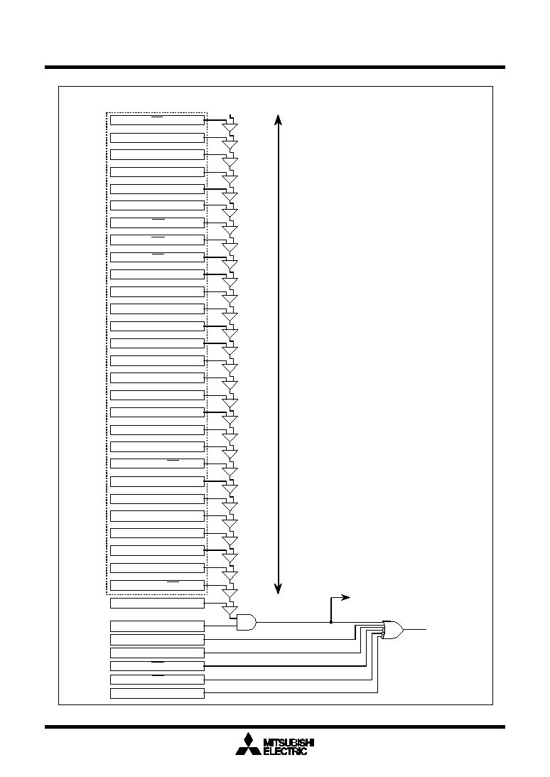
Mitsubishi microcomputers
M16C / 62A Group
SINGLE-CHIP 16-BIT CMOS MICROCOMPUTER
Interrupt
59
Figure 1.11.9. Maskable interrupts priorities (peripheral I/O interrupts)
Timer B2
Timer B0
Timer A3
Timer A1
Timer B1
Timer A4
Timer A2
UART1 reception
UART0 reception
UART2 reception/ACK
A-D conversion
DMA1
Bus collision detection
Timer A0
UART1 transmission
UART0 transmission
UART2 transmission/NACK
Key input interrupt
DMA0
Processor interrupt priority level (IPL)
Interrupt enable flag (I flag)
INT1
INT2
INT0
Watchdog timer
Reset
DBC
NMI
Interrupt
request
accepted
Level 0 (initial value)
Priority level of each interrupt
High
Low
Priority of peripheral I/O interrupts
(if priority levels are same)
Timer B4
INT3
Timer B3
Timer B5
Serial I/O4/INT5
Serial I/O3/INT4
Address match
Interrupt request level judgment output
to clock generating circuit (Fig.1.10.3)

Mitsubishi microcomputers
M16C / 62A Group
SINGLE-CHIP 16-BIT CMOS MICROCOMPUTER
______
INT Interrupt
60
______
INT Interrupt
________
________
INT0 to INT5 are triggered by the edges of external inputs. The edge polarity is selected using the polarity
select bit.
________
Of interrupt control registers, 0048
16
is used both as serial I/O4 and external interrupt INT5 input control
________
register, and 0049
16
is used both as serial I/O3 and as external interrupt INT4 input control register. Use the
interrupt request cause select bits - bits 6 and 7 of the interrupt request cause select register (035F
16
) - to
specify which interrupt request cause to select. After having set an interrupt request cause, be sure to clear
the corresponding interrupt request bit before enabling an interrupt.
Either of the interrupt control registers - 0048
16
, 0049
16
- has the polarity-switching bit. Be sure to set this bit
to "0" to select an serial I/O as the interrupt request cause.
As for external interrupt input, an interrupt can be generated both at the rising edge and at the falling edge
by setting "1" in the INTi interrupt polarity switching bit of the interrupt request cause select register
(035F
16
). To select both edges, set the polarity switching bit of the corresponding interrupt control register
to `falling edge' ("0").
Figure 1.11.10 shows the Interrupt request cause select register.
Figure 1.11.10. Interrupt request cause select register
Interrupt request cause select register
Bit name
Function
Bit symbol
W
R
Symbol
Address
When reset
IFSR
035F
16
00
16
IFSR0
b7
b6
b5
b4
b3
b2
b1
b0
INT0 interrupt polarity
switching bit
0 : SIO3
1 : INT4
0 : SIO4
1 : INT5
0 : One edge
1 : Two edges
0 : One edge
1 : Two edges
0 : One edge
1 : Two edges
0 : One edge
1 : Two edges
0 : One edge
1 : Two edges
INT1 interrupt polarity
switching bit
INT2 interrupt polarity
switching bit
INT3 interrupt polarity
switching bit
INT4 interrupt polarity
switching bit
INT5 interrupt polarity
switching bit
0 : One edge
1 : Two edges
Interrupt request cause
select bit
Interrupt request cause
select bit
IFSR1
IFSR2
IFSR3
IFSR4
IFSR5
IFSR6
IFSR7

Mitsubishi microcomputers
M16C / 62A Group
SINGLE-CHIP 16-BIT CMOS MICROCOMPUTER
________
NMI Interrupt
61
Interrupt control circuit
Key input interrupt control register
(address 004D
16
)
Key input interrupt
request
P10
7
/KI
3
P10
6
/KI
2
P10
5
/KI
1
P10
4
/KI
0
Port P10
4
-P10
7
pull-up
select bit
Port P10
7
direction
register
Pull-up
transistor
Port P10
7
direction register
Port P10
6
direction
register
Port P10
5
direction
register
Port P10
4
direction
register
Pull-up
transistor
Pull-up
transistor
Pull-up
transistor
Figure 1.11.11. Block diagram of key input interrupt
______
NMI Interrupt
______
______
______
An NMI interrupt is generated when the input to the P8
5
/NMI pin changes from "H" to "L". The NMI interrupt
is a non-maskable external interrupt. The pin level can be checked in the port P8
5
register (bit 5 at address
03F0
16
).
This pin cannot be used as a normal port input.
Key Input Interrupt
If the direction register of any of P10
4
to P10
7
is set for input and a falling edge is input to that port, a key
input interrupt is generated. A key input interrupt can also be used as a key-on wakeup function for cancel-
ling the wait mode or stop mode. However, if you intend to use the key input interrupt, do not use P10
4
to
P10
7
as A-D input ports. Figure 1.11.11 shows the block diagram of the key input interrupt. Note that if an
"L" level is input to any pin that has not been disabled for input, inputs to the other pins are not detected as
an interrupt.

Mitsubishi microcomputers
M16C / 62A Group
SINGLE-CHIP 16-BIT CMOS MICROCOMPUTER
Address Match Interrupt
62
Address Match Interrupt
An address match interrupt is generated when the address match interrupt address register contents match
the program counter value. Two address match interrupts can be set, each of which can be enabled and
disabled by an address match interrupt enable bit. Address match interrupts are not affected by the inter-
rupt enable flag (I flag) and processor interrupt priority level (IPL). For an address match interrupt, the value
of the program counter (PC) that is saved to the stack area varies depending on the instruction being
executed. Note that when using the external data bus in width of 8 bits, the address match interrupt cannot
be used for external area.
Figure 1.11.12 shows the address match interrupt-related registers.
Bit name
Bit symbol
Symbol
Address When
reset
AIER
0009
16
XXXXXX00
2
Address match interrupt enable register
Function
W
R
Address match interrupt 0
enable bit
0 : Interrupt disabled
1 : Interrupt enabled
AIER0
Address match interrupt 1
enable bit
AIER1
Symbol
Address
When reset
RMAD0
0012
16
to 0010
16
X00000
16
RMAD1
0016
16
to 0014
16
X00000
16
Nothing is assigned.
In an attempt to write to these bits, write "0". The value, if read, turns out to
be indeterminated.
b7
b6
b5
b4
b3
b2
b1
b0
W
R
Address setting register for address match interrupt
Function
Values that can be set
Address match interrupt register i (i = 0, 1)
00000
16
to FFFFF
16
Nothing is assigned.
In an attempt to write to these bits, write "0". The value, if read, turns out to
be indeterminated.
0 : Interrupt disabled
1 : Interrupt enabled
b0 b7
b0
b3
(b19)
(b16)
b7
b0
(b15)
(b8)
b7
(b23)
Figure 1.11.12. Address match interrupt-related registers

Mitsubishi microcomputers
M16C / 62A Group
SINGLE-CHIP 16-BIT CMOS MICROCOMPUTER
Precautions for Interrupts
63
Precautions for Interrupts
(1) Reading address 00000
16
∑ When maskable interrupt is occurred, CPU reads the interrupt information (the interrupt number and
interrupt request level) in the interrupt sequence.
The interrupt request bit of the certain interrupt written in address 00000
16
will then be set to "0".
Even if the address 00000
16
is read out by software, "0" is set to the enabled highest priority interrupt
source request bit. Therefore interrupt can be canceled and unexpected interrupt can occur.
Do not read address 00000
16
by software.
(2) Setting the stack pointer
∑ The value of the stack pointer immediately after reset is initialized to 0000
16
. Accepting an interrupt
before setting a value in the stack pointer may become a factor of runaway. Be sure to set a value in
_______
the stack pointer before accepting an interrupt. When using the NMI interrupt, initialize the stack
pointer at the beginning of a program. Concerning the first instruction immediately after reset, generat-
_______
ing any interrupts including the NMI interrupt is prohibited.
_______
(3) The NMI interrupt
_______
_______
∑The NMI interrupt can not be disabled. Be sure to connect NMI pin to Vcc via a pull-up resistor if
unused. Be sure to work on it.
_______
∑ The NMI pin also serves as P8
5
, which is exclusively input. Reading the contents of the P8 register
allows reading the pin value. Use the reading of this pin only for establishing the pin level at the time
_______
when the NMI interrupt is input.
_______
∑ Do not reset the CPU with the input to the NMI pin being in the "L" state.
_______
∑ Do not attempt to go into stop mode with the input to the NMI pin being in the "L" state. With the input to
_______
the NMI being in the "L" state, the CM10 is fixed to "0", so attempting to go into stop mode is turned
down.
_______
∑ Do not attempt to go into wait mode with the input to the NMI pin being in the "L" state. With the input to
_______
the NMI pin being in the "L" state, the CPU stops but the oscillation does not stop, so no power is saved.
In this instance, the CPU is returned to the normal state by a later interrupt.
_______
∑ Signals input to the NMI pin require an "L" level of 1 clock or more, from the operation clock of the CPU.
(4) External interrupt
________
∑ Either an "L" level or an "H" level of at least 250 ns width is necessary for the signal input to pins INT
0
________
through INT
5
regardless of the CPU operation clock.
________
________
∑ When the polarity of the INT
0
to INT
5
pins is changed, the interrupt request bit is sometimes set to "1".
After changing the polarity, set the interrupt request bit to "0". Figure 1.11.13 shows the procedure for
______
changing the INT interrupt generate factor.

Mitsubishi microcomputers
M16C / 62A Group
SINGLE-CHIP 16-BIT CMOS MICROCOMPUTER
Precautions for Interrupts
64
______
Figure 1.11.13. Switching condition of INT interrupt request
Set the interrupt priority level to level 0
(Disable INT
i
interrupt)
Set the polarity select bit
Clear the interrupt request bit to "0"
Set the interrupt priority level to level 1 to 7
(Enable the accepting of INTi interrupt request)
Clear the interrupt enable flag to "0"
(Disable interrupt)
Set the interrupt enable flag to "1"
(Enable interrupt)
Note: Execute the setting above individually. Don't execute two or
more settings at once(by one instruction).
Example 1:
INT_SWITCH1:
FCLR
I
; Disable interrupts.
AND.B
#00h, 0055h
; Clear TA0IC int. priority level and int. request bit.
NOP
; Four NOP instructions are required when using HOLD function.
NOP
FSET
I
; Enable interrupts.
Example 2:
INT_SWITCH2:
FCLR
I
; Disable interrupts.
AND.B
#00h, 0055h
; Clear TA0IC int. priority level and int. request bit.
MOV.W MEM, R0
; Dummy read.
FSET
I
; Enable interrupts.
Example 3:
INT_SWITCH3:
PUSHC FLG
; Push Flag register onto stack
FCLR
I
; Disable interrupts.
AND.B
#00h, 0055h
; Clear TA0IC int. priority level and int. request bit.
POPC
FLG
; Enable interrupts.
The reason why two NOP instructions (four when using the HOLD function) or dummy read are inserted
before FSET I in Examples 1 and 2 is to prevent the interrupt enable flag I from being set before the
interrupt control register is rewritten due to effects of the instruction queue.
(5) Rewrite the interrupt control register
∑ To rewrite the interrupt control register, do so at a point that does not generate the interrupt request for
that register. If there is possibility of the interrupt request occur, rewrite the interrupt control register after
the interrupt is disabled. The program examples are described as follow:
∑ When a instruction to rewrite the interrupt control register is executed but the interrupt is disabled, the
interrupt request bit is not set sometimes even if the interrupt request for that register has been gener-
ated. This will depend on the instruction. If this creates problems, use the below instructions to change
the register.
Instructions : AND, OR, BCLR, BSET

Mitsubishi microcomputers
M16C / 62A Group
SINGLE-CHIP 16-BIT CMOS MICROCOMPUTER
Watchdog Timer
65
Watchdog Timer
The watchdog timer has the function of detecting when the program is out of control. Therefore, we recom-
mend using the watchdog timer to improve reliability of a system.The watchdog timer is a 15-bit counter
which down-counts the clock derived by dividing the BCLK using the prescaler. A watchdog timer interrupt
is generated when an underflow occurs in the watchdog timer. When X
IN
is selected for the BCLK
,
bit 7 of
the watchdog timer control register (address 000F
16
) selects the prescaler division ratio (by 16 or by 128).
When X
CIN
is selected as the BCLK, the prescaler is set for division by 2 regardless of bit 7 of the watchdog
timer control register (address 000F
16
). Thus the watchdog timer's period can be calculated as given
below. The watchdog timer's period is, however, subject to an error due to the prescaler.
BCLK
Write to the watchdog timer
start register
(address 000E
16
)
RESET
Watchdog timer
interrupt request
Watchdog timer
Set to
"7FFF
16
"
1/128
1/16
"CM07 = 0"
"WDC7 = 1"
"CM07 = 0"
"WDC7 = 0"
"CM07 = 1"
HOLD
1/2
Prescaler
For example, suppose that BCLK runs at 16 MHz and that 16 has been chosen for the dividing ratio of the
prescaler, then the watchdog timer's period becomes approximately 32.8 ms.
The watchdog timer is initialized by writing to the watchdog timer start register (address 000E
16
) and when
a watchdog timer interrupt request is generated. The prescaler is initialized only when the microcomputer is
reset. After a reset is cancelled, the watchdog timer and prescaler are both stopped. The count is started by
writing to the watchdog timer start register (address 000E
16
). In stop mode, wait mode and hold state, the
watchdog timer and prescaler are stopped. Counting is resumed from the held value when the modes or
state are released.
Figure 1.12.1 shows the block diagram of the watchdog timer. Figure 1.12.2 shows the watchdog timer-
related registers.
With X
IN
chosen for BCLK
Watchdog timer period =
prescaler dividing ratio (16 or 128) X watchdog timer count (32768)
BCLK
Figure 1.12.1. Block diagram of watchdog timer
With X
CIN
chosen for BCLK
Watchdog timer period =
prescaler dividing ratio (2) X watchdog timer count (32768)
BCLK

Mitsubishi microcomputers
M16C / 62A Group
SINGLE-CHIP 16-BIT CMOS MICROCOMPUTER
Watchdog Timer
66
Watchdog timer control register
Symbol
Address
When reset
WDC
000F
16
000XXXXX
2
Function
Bit symbol
W
R
b7
b6
b5
b4
b3
b2
b1
b0
High-order bit of watchdog timer
WDC7
Bit name
Prescaler select bit
0 : Divided by 16
1 : Divided by 128
Watchdog timer start register
Symbol
Address
When reset
WDTS
000E
16
Indeterminate
W
R
b7
b0
Function
The watchdog timer is initialized and starts counting after a write instruction to
this register. The watchdog timer value is always initialized to "7FFF
16
"
regardless of whatever value is written.
Reserved bit
Reserved bit
Must always be set to "0"
Must always be set to "0"
0
0
Figure 1.12.2. Watchdog timer control and start registers

Mitsubishi microcomputers
M16C / 62A Group
SINGLE-CHIP 16-BIT CMOS MICROCOMPUTER
DMAC
67
DMAC
This microcomputer has two DMAC (direct memory access controller) channels that allow data to be sent to
memory without using the CPU. DMAC shares the same data bus with the CPU. The DMAC is given a
higher right of using the bus than the CPU, which leads to working the cycle stealing method. On this
account, the operation from the occurrence of DMA transfer request signal to the completion of 1-word (16-
bit) or 1-byte (8-bit) data transfer can be performed at high speed. Figure 1.13.1 shows the block diagram
of the DMAC. Table 1.13.1 shows the DMAC specifications. Figures 1.13.2 to 1.13.4 show the registers
used by the DMAC.
Figure 1.13.1. Block diagram of DMAC
Data bus low-order bits
DMA latch high-order bits
DMA latch low-order bits
DMA0 source pointer SAR0(20)
DMA0 destination pointer DAR0 (20)
DMA0 forward address pointer (20) (Note)
Data bus high-order bits
Address bus
DMA1 destination pointer DAR1 (20)
DMA1 source pointer SAR1 (20)
DMA1 forward address pointer (20) (Note)
DMA0 transfer counter reload register TCR0 (16)
DMA0 transfer counter TCR0 (16)
DMA1 transfer counter reload register TCR1 (16)
DMA1 transfer counter TCR1 (16)
(addresses 0029
16
, 0028
16
)
(addresses 0039
16
, 0038
16
)
(addresses 0022
16
to 0020
16
)
(addresses 0026
16
to 0024
16
)
(addresses 0032
16
to 0030
16
)
(addresses 0036
16
to 0034
16
)
Note: Pointer is incremented by a DMA request.
Either a write signal to the software DMA request bit or an interrupt request signal is used as a DMA transfer
request signal. But the DMA transfer is affected neither by the interrupt enable flag (I flag) nor by the
interrupt priority level. The DMA transfer doesn't affect any interrupts either.
If the DMAC is active (the DMA enable bit is set to 1), data transfer starts every time a DMA transfer request
signal occurs. If the cycle of the occurrences of DMA transfer request signals is higher than the DMA
transfer cycle, there can be instances in which the number of transfer requests doesn't agree with the
number of transfers. For details, see the description of the DMA request bit.

Mitsubishi microcomputers
M16C / 62A Group
SINGLE-CHIP 16-BIT CMOS MICROCOMPUTER
DMAC
68
Item
Specification
No. of channels
2 (cycle steal method)
Transfer memory space
∑ From any address in the 1M bytes space to a fixed address
∑ From a fixed address to any address in the 1M bytes space
∑ From a fixed address to a fixed address
(Note that DMA-related registers [0020
16
to 003F
16
] cannot be accessed)
Maximum No. of bytes transferred
128K bytes (with 16-bit transfers) or 64K bytes (with 8-bit transfers)
DMA request factors (Note)
________
________
Falling edge of INT0 or INT1 or both edge
Timer A0 to timer A4 interrupt requests
Timer B0 to timer B5 interrupt requests
UART0 transfer and reception interrupt requests
UART1 transfer and reception interrupt requests
UART2 transfer and reception interrupt requests
Serial I/O3, 4 interrpt requests
A-D conversion interrupt requests
Software triggers
Channel priority
DMA0 takes precedence if DMA0 and DMA1 requests are generated simultaneously
Transfer unit
8 bits or 16 bits
Transfer address direction
forward/fixed (forward direction cannot be specified for both source and
destination simultaneously)
Transfer mode
∑ Single transfer mode
After the transfer counter underflows, the DMA enable bit turns to
"0", and the DMAC turns inactive
∑ Repeat transfer mode
After the transfer counter underflows, the value of the transfer counter
reload register is reloaded to the transfer counter.
The DMAC remains active unless a "0" is written to the DMA enable bit.
DMA interrupt request generation timing When an underflow occurs in the transfer counter
Active
When the DMA enable bit is set to "1", the DMAC is active.
When the DMAC is active, data transfer starts every time a DMA
transfer request signal occurs.
Inactive
∑ When the DMA enable bit is set to "0", the DMAC is inactive.
∑ After the transfer counter underflows in single transfer mode
At the time of starting data transfer immediately after turning the DMAC active, the
value of one of source pointer and destination pointer - the one specified for the
forward direction - is reloaded to the forward direction address pointer, and the value
of the transfer counter reload register is reloaded to the transfer counter.
Writing to register
Registers specified for forward direction transfer are always write enabled.
Registers specified for fixed address transfer are write-enabled when
the DMA enable bit is "0".
Reading the register
Can be read at any time.
However, when the DMA enable bit is "1", reading the register set up as the
forward register is the same as reading the value of the forward address pointer.
Table 1.13.1. DMAC specifications
Note: DMA transfer is not effective to any interrupt. DMA transfer is affected neither by the interrupt enable
flag (I flag) nor by the interrupt priority level.
Reload timing for forward ad-
dress pointer and transfer
counter

Mitsubishi microcomputers
M16C / 62A Group
SINGLE-CHIP 16-BIT CMOS MICROCOMPUTER
DMAC
69
DMA0 request cause select register
Symbol
Address
When reset
DM0SL
03B8
16
00
16
Function
Bit symbol
b7
b6
b5
b4
b3
b2
b1
b0
DMA request cause
select bit
DSEL0
R
W
DSEL1
DSEL2
DSEL3
Nothing is assigned.
In an attempt to write to these bits, write "0". The value, if read, turns out to be "0".
Software DMA
request bit
If software trigger is selected, a
DMA request is generated by
setting this bit to "1" (When read,
the value of this bit is always "0")
DSR
b3 b2 b1 b0
0 0 0 0 : Falling edge of INT0 pin
0 0 0 1 : Software trigger
0 0 1 0 : Timer A0
0 0 1 1 : Timer A1
0 1 0 0 : Timer A2
0 1 0 1 : Timer A3
0 1 1 0 : Timer A4 (DMS=0)
/two edges of INT0 pin (DMS=1)
0 1 1 1 : Timer B0 (DMS=0)
Timer B3 (DMS=1)
1 0 0 0 : Timer B1 (DMS=0)
Timer B4 (DMS=1)
1 0 0 1 : Timer B2 (DMS=0)
Timer B5 (DMS=1)
1 0 1 0 : UART0 transmit
1 0 1 1 : UART0 receive
1 1 0 0 : UART2 transmit
1 1 0 1 : UART2 receive
1 1 1 0 : A-D conversion
1 1 1 1 : UART1 transmit
Bit name
DMA request cause
expansion select bit
DMS
0 : Normal
1 : Expanded cause
Figure 1.13.2. DMAC register (1)
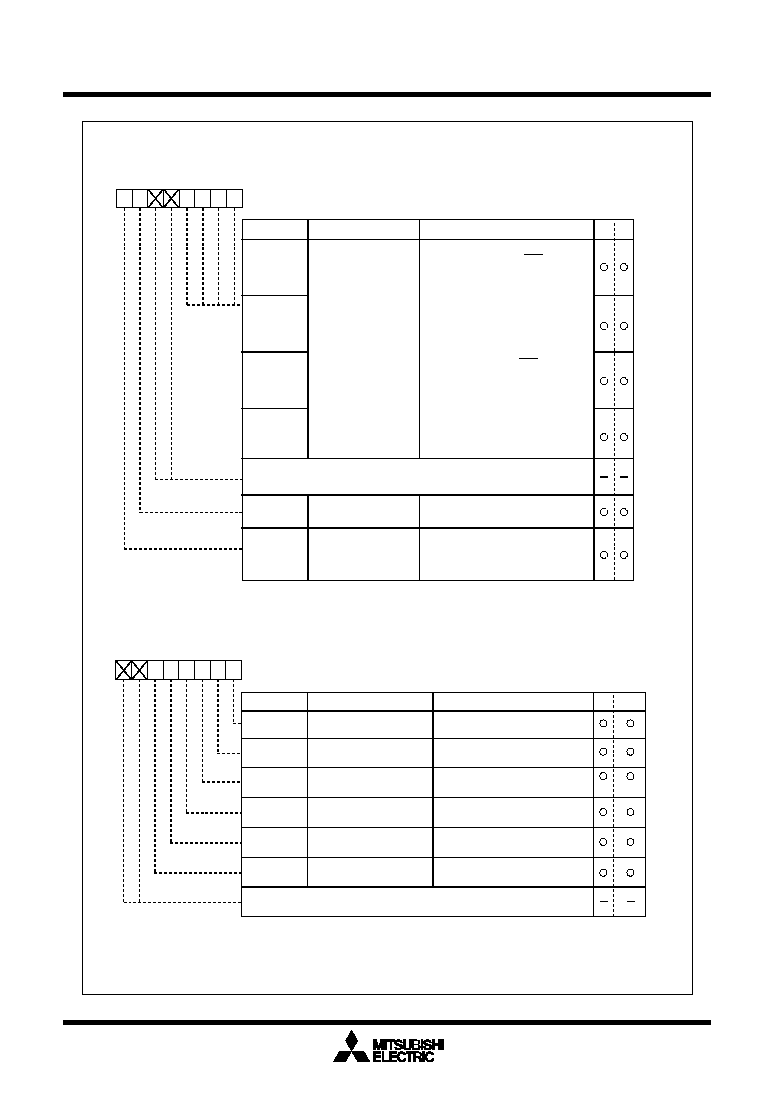
Mitsubishi microcomputers
M16C / 62A Group
SINGLE-CHIP 16-BIT CMOS MICROCOMPUTER
DMAC
70
DMAi control register
Symbol
Address
When reset
DMiCON(i=0,1)
002C
16
, 003C
16
00000X00
2
Bit name
Function
Bit symbol
Transfer unit bit select bit
b7
b6
b5
b4
b3
b2
b1
b0
0 : 16 bits
1 : 8 bits
DMBIT
R
W
DMASL
DMAS
DMAE
Repeat transfer mode
select bit
0 : Single transfer
1 : Repeat transfer
DMA request bit (Note 1)
0 : DMA not requested
1 : DMA requested
0 : Disabled
1 : Enabled
0 : Fixed
1 : Forward
DMA enable bit
Source address direction
select bit (Note 3)
Destination address
direction select bit (Note 3)
0 : Fixed
1 : Forward
DSD
DAD
Nothing is assigned.
In an attempt to write to these bits, write "0". The value, if read, turns out to be "0".
Note 1: DMA request can be cleared by resetting the bit.
Note 2: This bit can only be set to "0".
Note 3: Source address direction select bit and destination address direction select bit
cannot be set to "1" simultaneously.
(Note 2)
DMA1 request cause select register
Symbol
Address
When reset
DM1SL
03BA
16
00
16
Function
Bit symbol
b7
b6
b5
b4
b3
b2
b1
b0
DMA request cause
select bit
DSEL0
R
W
DSEL1
DSEL2
DSEL3
Nothing is assigned.
In an attempt to write to these bits, write "0". The value, if read, turns out to be "0".
Software DMA
request bit
If software trigger is selected, a
DMA request is generated by
setting this bit to "1" (When read,
the value of this bit is always "0")
DSR
b3 b2 b1 b0
0 0 0 0 : Falling edge of INT1 pin
0 0 0 1 : Software trigger
0 0 1 0 : Timer A0
0 0 1 1 : Timer A1
0 1 0 0 : Timer A2
0 1 0 1 : Timer A3(DMS=0)
/serial I/O3 (DMS=1)
0 1 1 0 : Timer A4 (DMS=0)
/serial I/O4 (DMS=1)
0 1 1 1 : Timer B0 (DMS=0)
/two edges of INT1 (DMS=1)
1 0 0 0 : Timer B1
1 0 0 1 : Timer B2
1 0 1 0 : UART0 transmit
1 0 1 1 : UART0 receive
1 1 0 0 : UART2 transmit
1 1 0 1 : UART2 receive
1 1 1 0 : A-D conversion
1 1 1 1 : UART1 receive
Bit name
DMA request cause
expansion select bit
DMS
0 : Normal
1 : Expanded cause
Figure 1.13.3. DMAC register (2)

Mitsubishi microcomputers
M16C / 62A Group
SINGLE-CHIP 16-BIT CMOS MICROCOMPUTER
DMAC
71
b7
b0
b7
b0
(b8)
(b15)
Function
R W
∑ Transfer counter
Set a value one less than the transfer count
Symbol
Address
When reset
TCR0
0029
16
, 0028
16
Indeterminate
TCR1
0039
16
, 0038
16
Indeterminate
DMAi transfer counter (i = 0, 1)
Transfer count
specification
0000
16
to FFFF
16
b7
(b23)
b3
b0
b7
b0
b7
b0
(b8)
(b16)(b15)
(b19)
Function
R W
∑ Source pointer
Stores the source address
Symbol
Address
When reset
SAR0
0022
16
to 0020
16
Indeterminate
SAR1
0032
16
to 0030
16
Indeterminate
DMAi source pointer (i = 0, 1)
Transfer address
specification
00000
16
to FFFFF
16
Nothing is assigned.
In an attempt to write to these bits, write "0". The value, if read, turns out to be "0".
Symbol
Address
When reset
DAR0
0026
16
to 0024
16
Indeterminate
DAR1
0036
16
to 0034
16
Indeterminate
b3
b0
b7
b0
b7
b0
(b8)
(b15)
(b16)
(b19)
Function
R W
∑ Destination pointer
Stores the destination address
DMAi destination pointer (i = 0, 1)
Transfer address
specification
00000
16
to FFFFF
16
b7
(b23)
Nothing is assigned.
In an attempt to write to these bits, write "0". The value, if read, turns out to be "0".
Figure 1.13.4. DMAC register (3)

Mitsubishi microcomputers
M16C / 62A Group
SINGLE-CHIP 16-BIT CMOS MICROCOMPUTER
DMAC
72
(1) Transfer cycle
The transfer cycle consists of the bus cycle in which data is read from memory or from the SFR area
(source read) and the bus cycle in which the data is written to memory or to the SFR area (destination
write). The number of read and write bus cycles depends on the source and destination addresses. In
memory expansion mode and microprocessor mode, the number of read and write bus cycles also de-
pends on the level of the BYTE pin. Also, the bus cycle itself is longer when software waits are inserted.
(a) Effect of source and destination addresses
When 16-bit data is transferred on a 16-bit data bus, and the source and destination both start at odd
addresses, there are one more source read cycle and destination write cycle than when the source
and destination both start at even addresses.
(b) Effect of BYTE pin level
When transferring 16-bit data over an 8-bit data bus (BYTE pin = "H") in memory expansion mode and
microprocessor mode, the 16 bits of data are sent in two 8-bit blocks. Therefore, two bus cycles are
required for reading the data and two are required for writing the data. Also, in contrast to when the
CPU accesses internal memory, when the DMAC accesses internal memory (internal ROM, internal
RAM, and SFR), these areas are accessed using the data size selected by the BYTE pin.
(c) Effect of software wait
When the SFR area or a memory area with a software wait is accessed, the number of cycles is
increased for the wait by 1 bus cycle. The length of the cycle is determined by BCLK.
Figure 1.13.5 shows the example of the transfer cycles for a source read. For convenience, the destina-
tion write cycle is shown as one cycle and the source read cycles for the different conditions are shown.
In reality, the destination write cycle is subject to the same conditions as the source read cycle, with the
transfer cycle changing accordingly. When calculating the transfer cycle, remember to apply the respec-
tive conditions to both the destination write cycle and the source read cycle. For example (2) in Figure
1.13.5, if data is being transferred in 16-bit units on an 8-bit bus, two bus cycles are required for both the
source read cycle and the destination write cycle.

Mitsubishi microcomputers
M16C / 62A Group
SINGLE-CHIP 16-BIT CMOS MICROCOMPUTER
DMAC
73
BCLK
Address
bus
RD signal
WR signal
Data
bus
CPU use
CPU use
CPU use
CPU use
Source
Source
Destination
Destination
Dummy
cycle
Dummy
cycle
(1) 8-bit transfers
16-bit transfers and the source address is even.
BCLK
Address
bus
RD signal
WR signal
Data
bus
CPU use
CPU use
CPU use
CPU use
Source
Source
Destination
Destination
Dummy
cycle
Dummy
cycle
(3) One wait is inserted into the source read under the conditions in (1)
BCLK
Address
bus
RD signal
WR signal
Data
bus
CPU use
CPU use
CPU use
CPU use
Source
Source
Destination
Destination
Dummy
cycle
Dummy
cycle
Source + 1
Source + 1
(2) 16-bit transfers and the source address is odd
Transferring 16-bit data on an 8-bit data bus (In this case, there are also two destination cycles).
BCLK
Address
bus
RD signal
WR signal
Data
bus
CPU use
CPU use
CPU use
CPU use
Source
Source
Destination
Destination
Dummy
cycle
Dummy
cycle
Source + 1
Source + 1
(4) One wait is inserted into the source read under the conditions in (2)
(When 16-bit data is transferred on an 8-bit data bus, there are two destination cycles).
Note: The same timing changes occur with the respective conditions at the destination as at the source.
Figure 1.13.5. Example of the transfer cycles for a source read
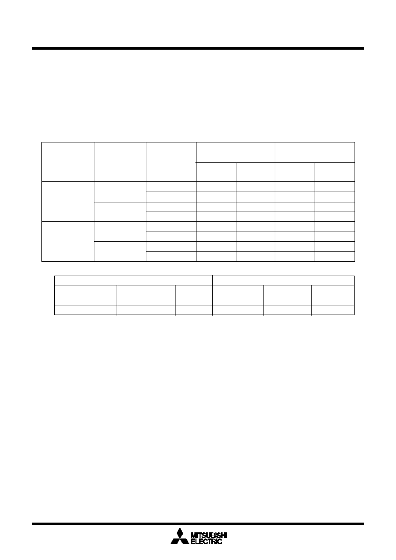
Mitsubishi microcomputers
M16C / 62A Group
SINGLE-CHIP 16-BIT CMOS MICROCOMPUTER
DMAC
74
Single-chip mode
Memory expansion mode
Transfer unit
Bus width
Access address
Microprocessor mode
No. of read
No. of write
No. of read No. of write
cycles
cycles
cycles
cycles
16-bit
Even
1
1
1
1
8-bit transfers
(BYTE= "L")
Odd
1
1
1
1
(DMBIT= "1")
8-bit
Even
--
--
1
1
(BYTE = "H")
Odd
--
--
1
1
16-bit
Even
1
1
1
1
16-bit transfers
(BYTE = "L")
Odd
2
2
2
2
(DMBIT= "0")
8-bit
Even
--
--
2
2
(BYTE = "H")
Odd
--
--
2
2
Table 1.13.2. No. of DMAC transfer cycles
Internal memory
External memory
Internal ROM/RAM
Internal ROM/RAM
SFR area
Separate bus
Separate bus
Multiplex
No wait
With wait
No wait
With wait
bus
1
2
2
1
2
3
Coefficient j, k
(2) DMAC transfer cycles
Any combination of even or odd transfer read and write addresses is possible. Table 1.13.2 shows the
number of DMAC transfer cycles.
The number of DMAC transfer cycles can be calculated as follows:
No. of transfer cycles per transfer unit = No. of read cycles x j + No. of write cycles x k

Mitsubishi microcomputers
M16C / 62A Group
SINGLE-CHIP 16-BIT CMOS MICROCOMPUTER
DMAC
75
DMA enable bit
Setting the DMA enable bit to "1" makes the DMAC active. The DMAC carries out the following operations
at the time data transfer starts immediately after DMAC is turned active.
(1) Reloads the value of one of the source pointer and the destination pointer - the one specified for the
forward direction - to the forward direction address pointer.
(2) Reloads the value of the transfer counter reload register to the transfer counter.
Thus overwriting "1" to the DMA enable bit with the DMAC being active carries out the operations given
above, so the DMAC operates again from the initial state at the instant "1" is overwritten to the DMA
enable bit.
DMA request bit
The DMAC can generate a DMA transfer request signal triggered by a factor chosen in advance out of
DMA request factors for each channel.
DMA request factors include the following.
* Factors effected by using the interrupt request signals from the built-in peripheral functions and software
DMA factors (internal factors) effected by a program.
* External factors effected by utilizing the input from external interrupt signals.
For the selection of DMA request factors, see the descriptions of the DMAi factor selection register.
The DMA request bit turns to "1" if the DMA transfer request signal occurs regardless of the DMAC's state
(regardless of whether the DMA enable bit is set to "1" or "0"). It turns to "0" immediately before data
transfer starts.
In addition, it can be set to "0" by use of a program, but cannot be set to "1".
There can be instances in which a change in DMA request factor selection bit causes the DMA request bit
to turn to "1". So be sure to set the DMA request bit to "0" after the DMA request factor selection bit is
changed.
The DMA request bit turns to "1" if a DMA transfer request signal occurs, and turns to "0" immediately
before data transfer starts. If the DMAC is active, data transfer starts immediately, so the value of the
DMA request bit, if read by use of a program, turns out to be "0" in most cases. To examine whether the
DMAC is active, read the DMA enable bit.
Here follows the timing of changes in the DMA request bit.
(1) Internal factors
Except the DMA request factors triggered by software, the timing for the DMA request bit to turn to "1" due
to an internal factor is the same as the timing for the interrupt request bit of the interrupt control register to
turn to "1" due to several factors.
Turning the DMA request bit to "0" due to an internal factor is timed to be effected immediately before the
transfer starts.
(2) External factors
_______
An external factor is a factor caused to occur by the leading edge of input from the INTi pin (i depends on
which DMAC channel is used).
_______
Selecting the INTi pins as external factors using the DMA request factor selection bit causes input from
these pins to become the DMA transfer request signals.
The timing for the DMA request bit to turn to "1" when an external factor is selected synchronizes with the
signal's edge applicable to the function specified by the DMA request factor selection bit (synchronizes
_______
with the trailing edge of the input signal to each INTi pin, for example).
With an external factor selected, the DMA request bit is timed to turn to "0" immediately before data
transfer starts similarly to the state in which an internal factor is selected.

Mitsubishi microcomputers
M16C / 62A Group
SINGLE-CHIP 16-BIT CMOS MICROCOMPUTER
DMAC
76
(3) The priorities of channels and DMA transfer timing
If a DMA transfer request signal falls on a single sampling cycle (a sampling cycle means one period from
the leading edge to the trailing edge of BCLK), the DMA request bits of applicable channels concurrently
turn to "1". If the channels are active at that moment, DMA0 is given a high priority to start data transfer.
When DMA0 finishes data transfer, it gives the bus right to the CPU. When the CPU finishes single bus
access, then DMA1 starts data transfer and gives the bus right to the CPU.
An example in which DMA transfer is carried out in minimum cycles at the time when DMA transfer
request signals due to external factors concurrently occur.
Figure 1.13.6 An example of DMA transfer effected by external factors.
BCLK
DMA0
DMA1
DMA0
request bit
DMA1
request bit
CPU
INT0
INT1
Obtainment
of the bus
right
An example in which DMA transmission is carried out in minimum
cycles at the time when DMA transmission request signals due to
external factors concurrently occur.
Figure 1.13.6. An example of DMA transfer effected by external factors

Mitsubishi microcomputers
M16C / 62A Group
SINGLE-CHIP 16-BIT CMOS MICROCOMPUTER
Timer
77
Timer
There are eleven 16-bit timers. These timers can be classified by function into timers A (five) and timers B
(six). All these timers function independently. Figures 1.14.1 and 1.14.2 show the block diagram of timers.
∑ Timer mode
∑ One-shot timer mode
∑ PWM mode
∑ Timer mode
∑ One-shot timer mode
∑ PWM mode
∑ Timer mode
∑ One-shot timer mode
∑ PWM mode
∑ Timer mode
∑ One-shot timer mode
∑ PWM mode
∑ Timer mode
∑ One-shot timer mode
∑ PWM mode
∑ Event counter mode
∑ Event counter mode
∑ Event counter mode
∑ Event counter mode
∑ Event counter mode
TA0
IN
TA1
IN
TA2
IN
TA3
IN
TA4
IN
Timer A0
Timer A1
Timer A2
Timer A3
Timer A4
f
1
f
8
f
32
f
C32
Timer A0 interrupt
Timer A1 interrupt
Timer A2 interrupt
Timer A3 interrupt
Timer A4 interrupt
Noise
filter
Noise
filter
Noise
filter
Noise
filter
Noise
filter
1/32
f
C32
1/8
1/4
f
1
f
8
f
32
X
IN
X
CIN
Clock prescaler reset flag (bit 7
at address 0381
16
) set to "1"
Reset
Clock prescaler
Timer B2 overflow
Note 1: The TA0
IN
pin (P7
1
) is shared with RxD
2
and the TB5
IN
pin, so be careful.
Figure 1.14.1. Timer A block diagram

Mitsubishi microcomputers
M16C / 62A Group
SINGLE-CHIP 16-BIT CMOS MICROCOMPUTER
Timer
78
Figure 1.14.2. Timer B block diagram
∑ Event counter mode
∑ Event counter mode
∑ Event counter mode
∑ Timer mode
∑ Pulse width measuring mode
∑ Timer mode
∑ Pulse width measuring mode
∑ Timer mode
∑ Pulse width measuring mode
TB0
IN
TB1
IN
TB2
IN
Timer B0
Timer B1
Timer B2
f
1
f
8
f
32
f
C32
Timer B0 interrupt
Noise
filter
Noise
filter
Noise
filter
1/32
f
C32
1/8
1/4
f
1
f
8
f
32
X
IN
X
CIN
Clock prescaler reset flag (bit 7
at address 0381
16
) set to "1"
Reset
Clock prescaler
Timer A
∑ Event counter mode
∑ Event counter mode
∑ Event counter mode
∑ Timer mode
∑ Pulse width measuring mode
∑ Timer mode
∑ Pulse width measuring mode
∑ Timer mode
∑ Pulse width measuring mode
TB3
IN
TB4
IN
TB5
IN
Timer B3
Timer B4
Timer B5
Timer B3 interrupt
Noise
filter
Noise
filter
Noise
filter
Timer B1 interrupt
Timer B2 interrupt
Timer B4 interrupt
Timer B5 interrupt
Note 1: The TB5
IN
pin (P7
1
) is shared with RxD
2
and the TA0
IN
pin, so be careful.

Mitsubishi microcomputers
M16C / 62A Group
SINGLE-CHIP 16-BIT CMOS MICROCOMPUTER
Timer A
79
Timer A
Figure 1.14.3 shows the block diagram of timer A. Figures 1.14.4 to 1.14.6 show the timer A-related
registers.
Except in event counter mode, timers A0 through A4 all have the same function. Use the timer Ai mode
register (i = 0 to 4) bits 0 and 1 to choose the desired mode.
Timer A has the four operation modes listed as follows:
∑ Timer mode: The timer counts an internal count source.
∑ Event counter mode: The timer counts pulses from an external source or a timer over flow.
∑ One-shot timer mode: The timer stops counting when the count reaches "0000
16
".
∑ Pulse width modulation (PWM) mode: The timer outputs pulses of a given width.
Figure 1.14.4. Timer A-related registers (1)
Count start flag
(Address 0380
16
)
Up count/down count
TAi
Addresses
TAj
TAk
Timer A0
0387
16
0386
16
Timer A4
Timer A1
Timer A1
0389
16
0388
16
Timer A0
Timer A2
Timer A2
038B
16
038A
16
Timer A1
Timer A3
Timer A3
038D
16
038C
16
Timer A2
Timer A4
Timer A4 038F
16
038E
16
Timer A3
Timer A0
Always down count except
in event counter mode
Reload register (16)
Counter (16)
Low-order
8 bits
High-order
8 bits
Clock source
selection
∑ Timer
(gate function)
∑ Timer
∑ One shot
∑ PWM
f
1
f
8
f
32
External
trigger
TAi
IN
(i = 0 to 4)
TB2 overflow
∑ Event counter
f
C32
Clock selection
TAj overflow
(j = i ≠ 1. Note, however, that j = 4 when i = 0)
Pulse output
Toggle flip-flop
TAi
OUT
(i = 0 to 4)
Data bus low-order bits
Data bus high-order bits
Up/down flag
Down count
(Address 0384
16
)
TAk overflow
(k = i + 1. Note, however, that k = 0 when i = 4)
Polarity
selection
Timer Ai mode register
Symbol
Address
When reset
TAiMR(i=0 to 4)
0396
16
to 039A
16
00
16
Bit name
Function
Bit symbol
W
R
b7
b6
b5
b4
b3
b2
b1
b0
0 0 : Timer mode
0 1 : Event counter mode
1 0 : One-shot timer mode
1 1 : Pulse width modulation
(PWM) mode
b1 b0
TCK1
MR3
MR2
MR1
TMOD1
MR0
TMOD0
TCK0
Function varies with each operation mode
Count source select bit
(Function varies with each operation mode)
Operation mode select bit
Figure 1.14.3. Block diagram of timer A

Mitsubishi microcomputers
M16C / 62A Group
SINGLE-CHIP 16-BIT CMOS MICROCOMPUTER
Timer A
80
Figure 1.14.5. Timer A-related registers (2)
Timer A4 up/down flag
Timer A3 up/down flag
Timer A2 up/down flag
Timer A1 up/down flag
Timer A0 up/down flag
Timer A2 two-phase pulse
signal processing select bit
Timer A3 two-phase pulse
signal processing select bit
Timer A4 two-phase pulse
signal processing select bit
Symbol
Address
When reset
UDF
0384
16
00
16
TA4P
TA3P
TA2P
Up/down flag (Note 1)
Bit name
Function
Bit symbol
W
R
b7
b6
b5
b4
b3
b2
b1
b0
TA4UD
TA3UD
TA2UD
TA1UD
TA0UD
0 : Down count
1 : Up count
This specification becomes valid
when the up/down flag content is
selected for up/down switching
cause
0 : two-phase pulse signal
processing disabled
1 : two-phase pulse signal
processing enabled (Note 2)
When not using the two-phase
pulse signal processing function,
set the select bit to "0"
Symbol
Address
When reset
TABSR
0380
16
00
16
Count start flag
Bit name
Function
Bit symbol
W
R
b7
b6
b5
b4
b3
b2
b1
b0
Timer B2 count start flag
Timer B1 count start flag
Timer B0 count start flag
Timer A4 count start flag
Timer A3 count start flag
Timer A2 count start flag
Timer A1 count start flag
Timer A0 count start flag
0 : Stops counting
1 : Starts counting
TB2S
TB1S
TB0S
TA4S
TA3S
TA2S
TA1S
TA0S
Symbol
Address
When reset
TA0
0387
16
,0386
16
Indeterminate
TA1
0389
16
,0388
16
Indeterminate
TA2
038B
16
,038A
16
Indeterminate
TA3
038D
16
,038C
16
Indeterminate
TA4
038F
16
,038E
16
Indeterminate
b7
b0 b7
b0
(b15)
(b8)
Timer Ai register (Note 1)
W
R
∑ Timer mode
0000
16
to FFFF
16
Counts an internal count source
Function
Values that can be set
∑ Event counter mode
0000
16
to FFFF
16
Counts pulses from an external source or timer overflow
∑ One-shot timer mode
0000
16
to FFFF
16
Counts a one shot width
(Note 2,4)
∑ Pulse width modulation mode (16-bit PWM)
Functions as a 16-bit pulse width modulator
∑ Pulse width modulation mode (8-bit PWM)
Timer low-order address functions as an 8-bit
prescaler and high-order address functions as an 8-bit
pulse width modulator
0000
16
to FFFE
16
(Note 3,4)
Note 1: Read and write data in 16-bit units.
Note 2: When the timer Ai register is set to "0000
16
", the counter does not
operate and the timer Ai interrupt request is not generated. When
the pulse is set to output, the pulse does not output from the TAi
OUT
pin.
Note 3: When the timer Ai register is set to "0000
16
", the pulse width
modulator does not operate and the output level of the TAi
OUT
pin
remains "L" level, therefore the timer Ai interrupt request is not
generated. This also occurs in the 8-bit pulse width modulator mode
when the significant 8 high-order bits in the timer Ai register are set
to "00
16
".
Note 4: Use MOV instruction to write to this register.
00
16
to FE
16
(High-order address)
00
16
to FF
16
(Low-order address)
(Note 3,4)
Note 1: Use MOV instruction to write to this register.
Note 2: Set the TAi
IN
and TAi
OUT
pins correspondent port direction registers to "0".

Mitsubishi microcomputers
M16C / 62A Group
SINGLE-CHIP 16-BIT CMOS MICROCOMPUTER
Timer A
81
Symbol
Address
When reset
CPSRF
0381
16
0XXXXXXX
2
Clock prescaler reset flag
Bit name
Function
Bit symbol
b7
b6
b5
b4
b3
b2
b1
b0
Clock prescaler reset flag
0 : No effect
1 : Prescaler is reset
(When read, the value is "0")
CPSR
W
R
Nothing is assigned.
In an attempt to write to these bits, write "0". The value, if read, turns out to be
indeterminate.
TA1TGL
Symbol
Address
When reset
TRGSR
0383
16
00
16
Timer A1 event/trigger
select bit
0 0 :
Input on TA1
IN
is selected (Note)
0 1 : TB2 overflow is selected
1 0 : TA0 overflow is selected
1 1 : TA2 overflow is selected
Trigger select register
Bit name
Function
Bit symbol
b7
b6
b5
b4
b3
b2
b1
b0
0 0 :
Input on TA2
IN
is selected (Note)
0 1 : TB2 overflow is selected
1 0 : TA1 overflow is selected
1 1 : TA3 overflow is selected
0 0 :
Input on TA3
IN
is selected (Note)
0 1 : TB2 overflow is selected
1 0 : TA2 overflow is selected
1 1 : TA4 overflow is selected
0 0 :
Input on TA4
IN
is selected (Note)
0 1 : TB2 overflow is selected
1 0 : TA3 overflow is selected
1 1 : TA0 overflow is selected
Timer A2 event/trigger
select bit
Timer A3 event/trigger
select bit
Timer A4 event/trigger
select bit
W
R
TA1TGH
TA2TGL
TA2TGH
TA3TGL
TA3TGH
TA4TGL
TA4TGH
b1 b0
b3 b2
b5 b4
b7 b6
Note: Set the corresponding port direction register to "0".
TA1OS
TA2OS
TA0OS
One-shot start flag
Symbol
Address
When reset
ONSF
0382
16
00X00000
2
Timer A0 one-shot start flag
Timer A1 one-shot start flag
Timer A2 one-shot start flag
Timer A3 one-shot start flag
Timer A4 one-shot start flag
TA3OS
TA4OS
Bit name
Function
Bit symbol
b7
b6
b5
b4
b3
b2
b1
b0
Nothing is assigned.
In an attempt to write to this bit, write "0". The value, if read, turns out to be indeterminate.
TA0TGL
TA0TGH
0 0 :
Input on TA0
IN
is selected (Note)
0 1 : TB2 overflow is selected
1 0 : TA4 overflow is selected
1 1 : TA1 overflow is selected
Timer A0 event/trigger
select bit
b7 b6
Note: Set the corresponding port direction register to "0".
W
R
1 : Timer start
When read, the value is "0"
Figure 1.14.6. Timer A-related registers (3)

Mitsubishi microcomputers
M16C / 62A Group
SINGLE-CHIP 16-BIT CMOS MICROCOMPUTER
Timer A
82
Item
Specification
Count source
f
1
, f
8
, f
32
, f
C32
Count operation
∑ Down count
∑ When the timer underflows, it reloads the reload register contents before continuing counting
Divide ratio
1/(n+1)
n : Set value
Count start condition
Count start flag is set (= 1)
Count stop condition
Count start flag is reset (= 0)
Interrupt request generation timing
When the timer underflows
TAi
IN
pin function
Programmable I/O port or gate input
TAi
OUT
pin function
Programmable I/O port or pulse output
Read from timer
Count value can be read out by reading timer Ai register
Write to timer
∑ When counting stopped
When a value is written to timer Ai register, it is written to both reload register and counter
∑ When counting in progress
When a value is written to timer Ai register, it is written to only reload register
(Transferred to counter at next reload time)
Select function
∑ Gate function
Counting can be started and stopped by the TAi
IN
pin's input signal
∑ Pulse output function
Each time the timer underflows, the TAi
OUT
pin's polarity is reversed
(1) Timer mode
In this mode, the timer counts an internally generated count source. (See Table 1.14.1.) Figure 1.14.7
shows the timer Ai mode register in timer mode.
Table 1.14.1. Specifications of timer mode
Note 1: The settings of the corresponding port register and port direction register
are invalid.
Note 2: The bit can be "0" or "1".
Note 3: Set the corresponding port direction register to "0".
Timer Ai mode register
Symbol
Address
When reset
TAiMR(i=0 to 4)
0396
16
to 039A
16
00
16
Bit name
Function
Bit symbol
W
R
b7
b6
b5
b4
b3
b2
b1
b0
Operation mode
select bit
0 0 : Timer mode
b1 b0
TMOD1
TMOD0
MR0
Pulse output function
select bit
0 : Pulse is not output
(TA
iOUT
pin is a normal port pin)
1 : Pulse is output (Note 1)
(TA
iOUT
pin is a pulse output pin)
Gate function select bit
0 X
(Note 2)
: Gate function not available
(TAi
IN
pin is a normal port pin)
1 0 : Timer counts only when TA
iIN
pin is
held "L" (Note 3)
1 1 : Timer counts only when TA
iIN
pin is
held "H" (Note 3)
b4 b3
MR2
MR1
MR3
0 (Must always be "0" in timer mode)
0 0 : f
1
0 1 : f
8
1 0 : f
32
1 1 : f
C32
b7 b6
TCK1
TCK0
Count source select bit
0 0
0
Figure 1.14.7. Timer Ai mode register in timer mode

Mitsubishi microcomputers
M16C / 62A Group
SINGLE-CHIP 16-BIT CMOS MICROCOMPUTER
Timer A
83
Item
Specification
Count source
∑ External signals input to TAi
IN
pin (effective edge can be selected by software)
∑ TB2 overflow, TAj overflow
Count operation
∑ Up count or down count can be selected by external signal or software
∑ When the timer overflows or underflows, it reloads the reload register con
tents before continuing counting (Note)
Divide ratio
1/ (FFFF
16
- n + 1) for up count
1/ (n + 1) for down count
n : Set value
Count start condition
Count start flag is set (= 1)
Count stop condition
Count start flag is reset (= 0)
Interrupt request generation timing The timer overflows or underflows
TAi
IN
pin function
Programmable I/O port or count source input
TAi
OUT
pin function
Programmable I/O port, pulse output, or up/down count select input
Read from timer
Count value can be read out by reading timer Ai register
Write to timer
∑ When counting stopped
When a value is written to timer Ai register, it is written to both reload register and counter
∑ When counting in progress
When a value is written to timer Ai register, it is written to only reload register
(Transferred to counter at next reload time)
Select function
∑ Free-run count function
Even when the timer overflows or underflows, the reload register content is not reloaded to it
∑ Pulse output function
Each time the timer overflows or underflows, the TAi
OUT
pin's polarity is reversed
Note: This does not apply when the free-run function is selected.
(2) Event counter mode
In this mode, the timer counts an external signal or an internal timer's overflow. Timers A0 and A1 can
count a single-phase external signal. Timers A2, A3, and A4 can count a single-phase and a two-phase
external signal. Table 1.14.2 lists timer specifications when counting a single-phase external signal.
Figure 1.14.8 shows the timer Ai mode register in event counter mode.
Table 1.14.3 lists timer specifications when counting a two-phase external signal. Figure 1.14.9 shows
the timer Ai mode register in event counter mode.
Table 1.14.2. Timer specifications in event counter mode (when not processing two-phase pulse signal)
Figure 1.14.8. Timer Ai mode register in event counter mode
Note 1: In event counter mode, the count source is selected by the event / trigger select bit
(addresses 0382
16
and 0383
16
).
Note 2: The settings of the corresponding port register and port direction register are invalid.
Note 3: Valid only when counting an external signal.
Note 4: When an "L" signal is input to the TAi
OUT
pin, the downcount is activated. When "H",
the upcount is activated. Set the corresponding port direction register to "0".
Symbol
Address
When reset
TAiMR(i = 0 to 4) 0396
16
to 039A
16
00
16
W
R
b7
b6
b5
b4
b3
b2
b1
b0
Operation mode select bit
0 1 : Event counter mode
(Note 1)
b1 b0
TMOD0
MR0
Pulse output function
select bit
0 : Pulse is not output
(TA
iOUT
pin is a normal port pin)
1 : Pulse is output (Note 2)
(TA
iOUT
pin is a pulse output pin)
Count polarity
select bit (Note 3)
MR2
MR1
MR3
0 (Must always be "0" in event counter mode)
TCK0
Count operation type
select bit
0 1
0
0 : Counts external signal's falling edge
1 : Counts external signal's rising edge
Up/down switching
cause select bit
0 : Up/down flag's content
1 : TA
iOUT
pin's input signal (Note 4)
0 : Reload type
1 : Free-run type
Bit symbol
Bit name
Function
R W
TCK1
Invalid when not using two-phase pulse signal processing
Can be "0" or "1"
TMOD1
Timer Ai mode register
(When not using two-phase pulse signal processing)

Mitsubishi microcomputers
M16C / 62A Group
SINGLE-CHIP 16-BIT CMOS MICROCOMPUTER
Timer A
84
Item
Specification
Count source
∑ Two-phase pulse signals input to TAi
IN
or TAi
OUT
pin
Count operation
∑ Up count or down count can be selected by two-phase pulse signal
∑ When the timer overflows or underflows, the reload register content is
reloaded and the timer starts over again (Note 1)
Divide ratio
1/ (FFFF
16
-
n + 1) for up count
1/ (n + 1) for down count
n : Set value
Count start condition
Count start flag is set (= 1)
Count stop condition
Count start flag is reset (= 0)
Interrupt request generation timing
Timer overflows or underflows
TAi
IN
pin function
Two-phase pulse input (Set the TAi
IN
pin correspondent port direction register to "0".)
TAi
OUT
pin function
Two-phase pulse input (Set the TAi
OUT
pin correspondent port direction register to "0".)
Read from timer
Count value can be read out by reading timer A2, A3, or A4 register
Write to timer
∑ When counting stopped
When a value is written to timer A2, A3, or A4 register, it is written to both
reload register and counter
∑ When counting in progress
When a value is written to timer A2, A3, or A4 register, it is written to only
reload register. (Transferred to counter at next reload time.)
Select function (Note 2)
∑ Normal processing operation (timer A2 and timer A3)
The timer counts up rising edges or counts down falling edges on the TAi
IN
pin when input signal on the TAi
OUT
pin is "H".
∑ Multiply-by-4 processing operation (timer A3 and timer A4)
If the phase relationship is such that the TAi
IN
pin goes "H" when the input
signal on the TAi
OUT
pin is "H", the timer counts up rising and falling edges
on the TAi
OUT
and TAi
IN
pins. If the phase relationship is such that the
TAi
IN
pin goes "L" when the input signal on the TAi
OUT
pin is "H", the timer
counts down rising and falling edges on the TAi
OUT
and TAi
IN
pins.
Note 1: This does not apply when the free-run function is selected.
Note 2: Timer A3 alone can be selected. Timer A2 is fixed to normal processing operation, and timer A4
is fixed to multiply-by-4 processing operation.
Table 1.14.3. Timer specifications in event counter mode (when processing two-phase pulse signal with timers A2, A3, and A4)
TAi
OUT
Up
count
Up
count
Up
count
Down
count
Down
count
Down
count
TAi
IN
(i=2,3)
TAi
OUT
TAi
IN
(i=3,4)
Count up all edges
Count up all edges
Count down all edges
Count down all edges

Mitsubishi microcomputers
M16C / 62A Group
SINGLE-CHIP 16-BIT CMOS MICROCOMPUTER
Timer A
85
Note 1: This bit is valid for timer A3 mode register. Timer A2 is fixed to normal processing
operation, and timer A4 is fixed to multiply-by-4 processing operation.
Note 2: When performing two-phase pulse signal processing, make sure the two-phase pulse
signal processing operation select bit (address 0384
16
) is set to "1". Also, always be
sure to set the event/trigger select bit (addresses 0382
16
and 0383
16
) to "00".
Timer Ai mode register
(When using two-phase pulse signal processing)
Symbol
Address
When reset
TAiMR(i = 2 to 4) 0398
16
to 039A
16
00
16
b6
b5
b4
b3
b2
b1
b0
Operation mode select bit
0 1 : Event counter mode
b1 b0
TMOD1
TMOD0
MR0
0 (Must always be "0" when using two-phase pulse signal
processing)
0 (Must always be "0" when using two-phase pulse signal
processing)
MR2
MR1
MR3
0 (Must always be "0" when using two-phase pulse signal
processing)
TCK1
TCK0
0 1
0
1 (Must always be "1" when using two-phase pulse signal
processing)
Bit name
Function
W
R
Count operation type
select bit
Two-phase pulse
processing operation
select bit (Note 1)(Note 2)
0 : Reload type
1 : Free-run type
0 : Normal processing operation
1 : Multiply-by-4 processing operation
0
0
1
Figure 1.14.9. Timer Ai mode register in event counter mode
Mitsubishi microcomputers
M16C / 62A Group
SINGLE-CHIP 16-BIT CMOS MICROCOMPUTER
Timer A
86
Item
Specification
Count source
f
1
, f
8
, f
32
, f
C32
Count operation
∑ The timer counts down
∑ When the count reaches 0000
16
, the timer stops counting after reloading a new count
∑ If a trigger occurs when counting, the timer reloads a new count and restarts counting
Divide ratio
1/n n : Set value
Count start condition
∑ An external trigger is input
∑ The timer overflows
∑ The one-shot start flag is set (= 1)
Count stop condition
∑ A new count is reloaded after the count has reached 0000
16
∑ The count start flag is reset (= 0)
Interrupt request generation timing
The count reaches 0000
16
TAi
IN
pin function
Programmable I/O port or trigger input
TAi
OUT
pin function
Programmable I/O port or pulse output
Read from timer
When timer Ai register is read, it indicates an indeterminate value
Write to timer
∑ When counting stopped
When a value is written to timer Ai register, it is written to both reload
register and counter
∑ When counting in progress
When a value is written to timer Ai register, it is written to only reload register
(Transferred to counter at next reload time)
Table 1.14.4. Timer specifications in one-shot timer mode
Figure 1.14.10. Timer Ai mode register in one-shot timer mode
(3) One-shot timer mode
In this mode, the timer operates only once. (See Table 1.14.4.) When a trigger occurs, the timer starts up
and continues operating for a given period. Figure 1.14.10 shows the timer Ai mode register in one-shot
timer mode.
Bit name
Timer Ai mode register
Symbol
Address
When reset
TAiMR(i = 0 to 4) 0396
16
to 039A
16
00
16
Function
Bit symbol
b7
b6
b5
b4
b3
b2
b1
b0
Operation mode select bit
1 0 : One-shot timer mode
b1 b0
TMOD1
TMOD0
MR0
Pulse output function
select bit
0 : Pulse is not output
(TA
iOUT
pin is a normal port pin)
1 : Pulse is output (Note 1)
(TAi
OUT
pin is a pulse output pin)
MR2
MR1
MR3
0 (Must always be "0" in one-shot timer mode)
0 0 : f
1
0 1 : f
8
1 0 : f
32
1 1 : f
C32
b7 b6
TCK1
TCK0
Count source select bit
1 0
0
0 : One-shot start flag is valid
1 : Selected by event/trigger select
bits
Trigger select bit
External trigger select
bit (Note 2)
0 : Falling edge of TAi
IN
pin's input signal (Note 3)
1 : Rising edge of TAi
IN
pin's input signal (Note 3)
Note 1: The settings of the corresponding port register and port direction register are invalid.
Note 2: Valid only when the TAi
IN
pin is selected by the event/trigger select bit
(addresses 0382
16
and 0383
16
). If timer overflow is selected, this bit can be "1" or "0".
Note 3: Set the corresponding port direction register to "0".
W
R

Mitsubishi microcomputers
M16C / 62A Group
SINGLE-CHIP 16-BIT CMOS MICROCOMPUTER
Timer A
87
(4) Pulse width modulation (PWM) mode
In this mode, the timer outputs pulses of a given width in succession. (See Table 1.14.5.) In this mode, the
counter functions as either a 16-bit pulse width modulator or an 8-bit pulse width modulator. Figure
1.14.11 shows the timer Ai mode register in pulse width modulation mode. Figure 1.14.12 shows the
example of how a 16-bit pulse width modulator operates. Figure 1.14.13 shows the example of how an 8-
bit pulse width modulator operates.
Figure 1.14.11. Timer Ai mode register in pulse width modulation mode
Table 1.14.5. Timer specifications in pulse width modulation mode
Bit name
Timer Ai mode register
Symbol
Address
When reset
TAiMR(i=0 to 4)
0396
16
to 039A
16
00
16
Function
Bit symbol
b7
b6
b5
b4
b3
b2
b1
b0
Operation mode
select bit
1 1 : PWM mode
b1 b0
TMOD1
TMOD0
MR0
MR2
MR1
MR3
0 0 : f
1
0 1 : f
8
1 0 : f
32
1 1 : f
C32
b7 b6
TCK1
TCK0
Count source select bit
W
R
1
1
1
1 (Must always be "1" in PWM mode)
16/8-bit PWM mode
select bit
0: Functions as a 16-bit pulse width modulator
1: Functions as an 8-bit pulse width modulator
Trigger select bit
External trigger select
bit (Note 1)
0: Falling edge of TAi
IN
pin's input signal (Note 2)
1: Rising edge of TAi
IN
pin's input signal (Note 2)
0: Count start flag is valid
1: Selected by event/trigger select bits
Note 1: Valid only when the TA
iIN
pin is selected by the event/trigger select bit
(addresses 0382
16
and 0383
16
). If timer overflow is selected, this bit can be "1" or "0".
Note 2: Set the corresponding port direction register to "0".
Item
Specification
Count source
f
1
, f
8
, f
32
, f
C32
Count operation
∑ The timer counts down (operating as an 8-bit or a 16-bit pulse width modulator)
∑ The timer reloads a new count at a rising edge of PWM pulse and continues counting
∑ The timer is not affected by a trigger that occurs when counting
16-bit PWM
∑ High level width
n / fi
n : Set value
∑ Cycle time
(2
16
-1) / fi fixed
8-bit PWM
∑ High level width n (m+1) / fi
n : values set to timer Ai register's high-order address
∑ Cycle time
(2
8
-1) (m+1) / fi
m : values set to timer Ai register's low-order address
Count start condition
∑ External trigger is input
∑ The timer overflows
∑ The count start flag is set (= 1)
Count stop condition
∑ The count start flag is reset (= 0)
Interrupt request generation timing
PWM pulse goes "L"
TAi
IN
pin function
Programmable I/O port or trigger input
TAi
OUT
pin function
Pulse output
Read from timer
When timer Ai register is read, it indicates an indeterminate value
Write to timer
∑ When counting stopped
When a value is written to timer Ai register, it is written to both reload
register and counter
∑ When counting in progress
When a value is written to timer Ai register, it is written to only reload register
(Transferred to counter at next reload time)

Mitsubishi microcomputers
M16C / 62A Group
SINGLE-CHIP 16-BIT CMOS MICROCOMPUTER
Timer A
88
1 / f
i
X
(2 ≠ 1)
16
Count source
TA
iIN
pin
input signal
PWM pulse output
from TA
iOUT
pin
Condition : Reload register = 0003
16
, when external trigger
(rising edge of TA
iIN
pin input signal) is selected
Trigger is not generated by this signal
"H"
"H"
"L"
"L"
Timer Ai interrupt
request bit
"1"
"0"
Cleared to "0" when interrupt request is accepted, or cleared by software
f
i
: Frequency of count source
(f
1
, f
8
, f
32
, f
C32
)
Note: n = 0000
16
to FFFE
16
.
1 / f
i
X
n
Count source (Note1)
TA
iIN
pin input signal
Underflow signal of
8-bit prescaler (Note2)
PWM pulse output
from TA
iOUT
pin
"H"
"H"
"H"
"L"
"L"
"L"
"1"
"0"
Timer Ai interrupt
request bit
Cleared to "0" when interrupt request is accepted, or cleaerd by software
f
i
: Frequency of count source
(f
1
, f
8
, f
32
, f
C32
)
Note 1: The 8-bit prescaler counts the count source.
Note 2: The 8-bit pulse width modulator counts the 8-bit prescaler's underflow signal.
Note 3: m = 00
16
to FF
16
; n = 00
16
to FE
16
.
Condition : Reload register high-order 8 bits = 02
16
Reload register low-order 8 bits = 02
16
External trigger (falling edge of TA
iIN
pin input signal) is selected
1 / f
i
X (m
+ 1) X (2 ≠ 1)
8
1 / f
i
X (m + 1) X n
1 / f
i
X (m + 1)
Figure 1.14.12. Example of how a 16-bit pulse width modulator operates
Figure 1.14.13. Example of how an 8-bit pulse width modulator operates

Mitsubishi microcomputers
M16C / 62A Group
SINGLE-CHIP 16-BIT CMOS MICROCOMPUTER
Timer B
89
Timer B
Figure 1.14.14 shows the block diagram of timer B. Figures 1.14.15 and 1.14.16 show the timer B-related
registers.
Use the timer Bi mode register (i = 0 to 5) bits 0 and 1 to choose the desired mode.
Timer B has three operation modes listed as follows:
∑ Timer mode: The timer counts an internal count source.
∑ Event counter mode: The timer counts pulses from an external source or a timer overflow.
∑ Pulse period/pulse width measuring mode: The timer measures an external signal's pulse period or
pulse width.
Figure 1.14.14. Block diagram of timer B
Timer Bi mode register
Symbol
Address
When reset
TBiMR(i = 0 to 5) 039B
16
to 039D
16
00XX0000
2
035B
16
to 035D
16
00XX0000
2
Bit name
Function
Bit symbol
W
R
b7
b6
b5
b4
b3
b2
b1
b0
0 0 : Timer mode
0 1 : Event counter mode
1 0 : Pulse period/pulse width
measurement mode
1 1 : Must not be set.
b1 b0
TCK1
MR3
MR2
MR1
TMOD1
MR0
TMOD0
TCK0
Function varies with each operation mode
Count source select bit
(Function varies with each operation mode)
Operation mode select bit
(Note 1)
(Note 2)
Note 1: Timer B0, timer B3.
Note 2: Timer B1, timer B2, timer B4, timer B5.
Clock source selection
(address 0380
16
)
∑ Event counter
∑ Timer
∑ Pulse period/pulse width measurement
Reload register (16)
Low-order 8 bits
High-order 8 bits
Data bus low-order bits
Data bus high-order bits
f
1
f
8
f
32
TBj overflow
(j = i ≠ 1. Note, however,
j = 2 when i = 0,
j = 5 when i = 3)
Can be selected in only
event counter mode
Count start flag
f
C32
Polarity switching
and edge pulse
TBi
IN
(i = 0 to 5)
Counter reset circuit
Counter (16)
TBi Address
TBj
Timer B0 0391
16
0390
16
Timer B2
Timer B1 0393
16
0392
16
Timer B0
Timer B2 0395
16
0394
16
Timer B1
Timer B3 0351
16
0350
16
Timer B5
Timer B4 0353
16
0352
16
Timer B3
Timer B5 0355
16
0354
16
Timer B4
Figure 1.14.15. Timer B-related registers (1)
Mitsubishi microcomputers
M16C / 62A Group
SINGLE-CHIP 16-BIT CMOS MICROCOMPUTER
Timer B
90
Symbol
Address
When reset
TABSR
0380
16
00
16
Count start flag
Bit name
Bit symbol
W
R
b7
b6
b5
b4
b3
b2
b1
b0
Timer B2 count start flag
Timer B1 count start flag
Timer B0 count start flag
Timer A4 count start flag
Timer A3 count start flag
Timer A2 count start flag
Timer A1 count start flag
Timer A0 count start flag
0 : Stops counting
1 : Starts counting
TB2S
TB1S
TB0S
TA4S
TA3S
TA2S
TA1S
TA0S
Function
Symbol
Address
When reset
CPSRF
0381
16
0XXXXXXX
2
Clock prescaler reset flag
Bit name
Function
Bit symbol
W
R
b7
b6
b5
b4
b3
b2
b1
b0
Clock prescaler reset flag
0 : No effect
1 : Prescaler is reset
(When read, the value is "0")
CPSR
Symbol
Address
When reset
TB0
0391
16
, 0390
16
Indeterminate
TB1
0393
16
, 0392
16
Indeterminate
TB2
0395
16
, 0394
16
Indeterminate
TB3
0351
16
, 0350
16
Indeterminate
TB4
0353
16
, 0352
16
Indeterminate
TB5
0355
16
, 0354
16
Indeterminate
b7
b0 b7
b0
(b15)
(b8)
Timer Bi register (Note)
W
R
∑ Pulse period / pulse width measurement mode
Measures a pulse period or width
∑ Timer mode
0000
16
to FFFF
16
Counts the timer's period
Function
Values that can be set
∑ Event counter mode
0000
16
to FFFF
16
Counts external pulses input or a timer overflow
Note: Read and write data in 16-bit units.
Symbol
Address
When reset
TBSR
0340
16
000XXXXX
2
Timer B3, 4, 5 count start flag
Bit name
Bit symbol
W
R
b7
b6
b5
b4
b3
b2
b1
b0
Timer B5 count start flag
Timer B4 count start flag
Timer B3 count start flag
0 : Stops counting
1 : Starts counting
TB5S
TB4S
TB3S
Nothing is assigned.
In an attempt to write to these bits, write "0". The value, if read, turns
out to be indeterminate.
Function
Nothing is assigned.
In an attempt to write to these bits, write "0". The value, if read, turns
out to be indeterminate.
Figure 1.14.16. Timer B-related registers (2)

Mitsubishi microcomputers
M16C / 62A Group
SINGLE-CHIP 16-BIT CMOS MICROCOMPUTER
Timer B
91
Item
Specification
Count source
f
1
, f
8
, f
32
, f
C32
Count operation
∑ Counts down
∑ When the timer underflows, it reloads the reload register contents before
continuing counting
Divide ratio
1/(n+1)
n : Set value
Count start condition
Count start flag is set (= 1)
Count stop condition
Count start flag is reset (= 0)
Interrupt request generation timing
The timer underflows
TBi
IN
pin function
Programmable I/O port
Read from timer
Count value is read out by reading timer Bi register
Write to timer
∑ When counting stopped
When a value is written to timer Bi register, it is written to both reload register and counter
∑ When counting in progress
When a value is written to timer Bi register, it is written to only reload register
(Transferred to counter at next reload time)
(1) Timer mode
In this mode, the timer counts an internally generated count source. (See Table 1.14.6.) Figure 1.14.17
shows the timer Bi mode register in timer mode.
Table 1.14.6. Timer specifications in timer mode
Note 1: Timer B0, timer B3.
Note 2: Timer B1, timer B2, timer B4, timer B5.
Timer Bi mode register
Symbol
Address
When reset
TBiMR(i=0 to 5)
039B
16
to 039D
16
00XX0000
2
035B
16
to 035D
16
00XX0000
2
Bit name
Function
Bit symbol
W
R
b7
b6
b5
b4
b3
b2
b1
b0
Operation mode select bit
0 0 : Timer mode
b1 b0
TMOD1
TMOD0
MR0
Invalid in timer mode
Can be "0" or "1"
MR2
MR1
MR3
0 0 : f
1
0 1 : f
8
1 0 : f
32
1 1 : f
C32
TCK1
TCK0
Count source select bit
0
Invalid in timer mode.
In an attempt to write to this bit, write "0". The value, if read in
timer mode, turns out to be indeterminate.
0
0 (Fixed to "0" in timer mode ; i = 0, 3)
Nothing is assiigned (i = 1, 2, 4, 5).
In an attempt to write to this bit, write "0". The value, if read, turns out
to be indeterminate.
(Note 1)
(Note 2)
b7 b6
Figure 1.14.17. Timer Bi mode register in timer mode

Mitsubishi microcomputers
M16C / 62A Group
SINGLE-CHIP 16-BIT CMOS MICROCOMPUTER
Timer B
92
Item
Specification
Count source
∑ External signals input to TBi
IN
pin
∑ Effective edge of count source can be a rising edge, a falling edge, or falling
and rising edges as selected by software
Count operation
∑ Counts down
∑ When the timer underflows, it reloads the reload register contents before
continuing counting
Divide ratio
1/(n+1)
n : Set value
Count start condition
Count start flag is set (= 1)
Count stop condition
Count start flag is reset (= 0)
Interrupt request generation timing The timer underflows
TBi
IN
pin function
Count source input
Read from timer
Count value can be read out by reading timer Bi register
Write to timer
∑ When counting stopped
When a value is written to timer Bi register, it is written to both reload register and counter
∑ When counting in progress
When a value is written to timer Bi register, it is written to only reload register
(Transferred to counter at next reload time)
(2) Event counter mode
In this mode, the timer counts an external signal or an internal timer's overflow. (See Table 1.14.7.)
Figure 1.14.18 shows the timer Bi mode register in event counter mode.
Table 1.14.7. Timer specifications in event counter mode
Figure 1.14.18. Timer Bi mode register in event counter mode
Timer Bi mode register
Symbol
Address
When reset
TBiMR(i=0 to 5)
039B
16
to 039D
16
00XX0000
2
035B
16
to 035D
16
00XX0000
2
Bit name
Function
Bit symbol
W
R
b7
b6
b5
b4
b3
b2
b1
b0
Operation mode select bit
0 1 : Event counter mode
b1 b0
TMOD1
TMOD0
MR0
Count polarity select
bit
(Note 1)
MR2
MR1
MR3
Invalid in event counter mode.
In an attempt to write to this bit, write "0". The value, if read in
event counter mode, turns out to be indeterminate.
TCK1
TCK0
0 1
0 0 : Counts external signal's
falling edges
0 1 : Counts external signal's
rising edges
1 0 : Counts external signal's
falling and rising edges
1 1 : Must not be set.
b3 b2
Nothing is assigned (i = 1, 2, 4, 5).
In an attempt to write to this bit, write "0". The value, if read,
turns out to be indeterminate.
Note 1: Valid only when input from the TBi
IN
pin is selected as the event clock.
If timer's overflow is selected, this bit can be "0" or "1".
Note 2: Timer B0, timer B3.
Note 3: Timer B1, timer B2, timer B4, timer B5.
Note 4: Set the corresponding port direction register to "0".
Invalid in event counter mode.
Can be "0" or "1".
Event clock select
0 : Input from TBi
IN
pin (Note 4)
1 : TBj overflow
(j = i ≠ 1; however, j = 2 when i = 0,
j = 5 when i = 3)
0 (Fixed to "0" in event counter mode; i = 0, 3)
(Note 2)
(Note 3)

Mitsubishi microcomputers
M16C / 62A Group
SINGLE-CHIP 16-BIT CMOS MICROCOMPUTER
Timer B
93
Item
Specification
Count source
f
1
, f
8
, f
32
, f
C32
Count operation
∑ Up count
∑ Counter value "0000
16
" is transferred to reload register at measurement
pulse's effective edge and the timer continues counting
Count start condition
Count start flag is set (= 1)
Count stop condition
Count start flag is reset (= 0)
Interrupt request generation timing ∑ When measurement pulse's effective edge is input
(Note 1)
∑ When an overflow occurs. (Simultaneously, the timer Bi overflow flag
changes to "1". The timer Bi overflow flag changes to "0" when the count
start flag is "1" and a value is written to the timer Bi mode register.)
TBi
IN
pin function
Measurement pulse input
Read from timer
When timer Bi register is read, it indicates the reload register's content
(measurement result)
(Note 2)
Write to timer
Cannot be written to
(3) Pulse period/pulse width measurement mode
In this mode, the timer measures the pulse period or pulse width of an external signal. (See Table 1.14.8.)
Figure 1.14.19 shows the timer Bi mode register in pulse period/pulse width measurement mode. Figure
1.14.20 shows the operation timing when measuring a pulse period. Figure 1.14.21 shows the operation
timing when measuring a pulse width.
Table 1.14.8. Timer specifications in pulse period/pulse width measurement mode
Figure 1.14.19. Timer Bi mode register in pulse period/pulse width measurement mode
Note 1: An interrupt request is not generated when the first effective edge is input after the timer has started counting.
Note 2: The value read out from the timer Bi register is indeterminate until the second effective edge is input
after the timer has started counting.
Timer Bi mode register
Symbol
Address
When reset
TBiMR(i=0 to 5)
039B
16
to 039D
16
00XX0000
2
035B
16
to 035D
16
00XX0000
2
Bit name
Bit symbol
W
R
b7
b6
b5
b4
b3
b2
b1
b0
Operation mode
select bit
1 0 : Pulse period / pulse width
measurement mode
b1 b0
TMOD1
TMOD0
MR0
Measurement mode
select bit
MR2
MR1
MR3
TCK1
TCK0
0
1
0 0 : Pulse period measurement (Interval between
measurement pulse's falling edge to falling edge)
0 1 : Pulse period measurement (Interval between
measurement pulse's rising edge to rising edge)
1 0 : Pulse width measurement (Interval between
measurement pulse's falling edge to rising edge,
and between rising edge to falling edge)
1 1 : Must not be set.
Function
b3 b2
Nothing is assigned (i = 1, 2, 4, 5).
In an attempt to write to this bit, write "0". The value, if read, turns out to be
indeterminate.
Count source
select bit
Timer Bi overflow
flag ( Note 1)
0 : Timer did not overflow
1 : Timer has overflowed
0 0 : f
1
0 1 : f
8
1 0 : f
32
1 1 : f
C32
b7 b6
Note 1: It is indeterminate when reset. The timer Bi overflow flag changes to "0" when the count start flag is "1"
and a value is written to the timer Bi mode register. This flag cannot be set to "1" by software.
Note 2: Timer B0, timer B3.
Note 3: Timer B1, timer B2, timer B4, timer B5.
0 (Fixed to "0" in pulse period/pulse width measurement mode; i = 0, 3)
(Note 2)
(Note 3)

Mitsubishi microcomputers
M16C / 62A Group
SINGLE-CHIP 16-BIT CMOS MICROCOMPUTER
Timer B
94
Figure 1.14.21. Operation timing when measuring a pulse width
Measurement pulse
"H"
Count source
Count start flag
Timer Bi interrupt
request bit
Timing at which counter
reaches "0000
16
"
"1"
"1"
Transfer
(measured value)
Transfer
(measured value)
"L"
"0"
"0"
Timer Bi overflow flag
"1"
"0"
Note 1: Counter is initialized at completion of measurement.
Note 2: Timer has overflowed.
(Note 1)
(Note 1)
(Note 1)
Transfer
(measured
value)
(Note 1)
Cleared to "0" when interrupt request is accepted, or cleared by software.
(Note 2)
Transfer
(indeterminate
value)
Reload register counter
transfer timing
Figure 1.14.20. Operation timing when measuring a pulse period
Count source
Measurement pulse
Count start flag
Timer Bi interrupt
request bit
Timing at which counter
reaches "0000
16
"
"H"
"1"
Transfer
(indeterminate value)
"L"
"0"
"0"
Timer Bi overflow flag
"1"
"0"
Note 1: Counter is initialized at completion of measurement.
Note 2: Timer has overflowed.
(Note 1)
(Note 1)
When measuring measurement pulse time interval from falling edge to falling edge
(Note 2)
Cleared to "0" when interrupt request is accepted, or cleared by software.
Transfer
(measured value)
"1"
Reload register counter
transfer timing

Mitsubishi microcomputers
M16C / 62A Group
SINGLE-CHIP 16-BIT CMOS MICROCOMPUTER
Timers' functions for three-phase motor control
95
Timers' functions for three-phase motor control
Use of more than one built-in timer A and timer B provides the means of outputting three-phase motor
driving waveforms.
Figures 1.15.1 to 1.15.3 show registers related to timers for three-phase motor control.
Three-phase PWM control register 0
Symbol
Address
When reset
INVC0
0348
16
00
16
b7
b6
b5
b4 b3
b2
b1
b0
Effective interrupt output
polarity select bit
INV00
Bit symbol
Bit name
Description
R
W
INV01
Effective interrupt output
specification bit
(Note 4)
INV02
Mode select bit
(Note 2)
INV04
Positive and negative
phases concurrent L
output disable function
enable bit
INV07
Software trigger bit
INV06
Modulation mode select
bit (Note 3)
INV05
Positive and negative
phases concurrent L
output detect flag
INV03
Output control
bit
0: A timer B2 interrupt occurs when the timer
A1 reload control signal is "1".
1: A timer B2 interrupt occurs when the timer
A1 reload control signal is "0".
Effective only in three-phase mode 1
0: Not specified.
1: Selected by the effective interrupt output
polarity selection bit.
Effective only in three-phase mode 1
0: Normal mode
1: Three-phase PWM output mode
0: Output disabled
1: Output enabled
0: Feature disabled
1: Feature enabled
0: Not detected yet
1: Already detected
0: Triangular wave modulation mode
1: Sawtooth wave modulation mode
1: Trigger generated
The value, when read, is "0".
(Note 1)
T
hree-phase PWM control register 1
Symbol
Address When
reset
INVC1
0349
16
00
16
Bit name
Description
Bit symbol
W
R
INV10
INV11
INV12
Timer Ai start trigger
signal select bit
Timer A1-1, A2-1, A4-1
control bit
Short circuit timer count
source select bit
0: Timer B2 overflow signal
1: Timer B2 overflow signal,
signal for writing to timer B2
0: Three-phase mode 0
1: Three-phase mode 1
0 : Must not be set.
1 : f
1
/2 (Note)
b7 b6
b5
b4
b3
b2
b1 b0
Noting is assigned.
In an attempt to write to these bits, write "0". The value, if read, turns out to be "0".
Noting is assigned.
In an attempt to write to this bit, write "0". The value, if read, turns out to be "0".
Reserved bit
Always set to "0"
0
Note : To use three-phase PWM output mode, write "1" to INV12.
Note 1:
Note 2:
Note 3:
Note 4:
No value other than "0" can be written.
Selecting three-phase PWM output mode causes P8
0
, P8
1
, and P7
2
through P7
5
to output U, U, V, V, W, and W, and works the
timer for setting short circuit prevention time, the U, V, W phase output control circuits, and the circuit for setting timer B2 interrupt
frequency.
In triangular wave modulation mode:
The short circuit prevention timer starts in synchronization with the falling edge of timer Ai output.
The data transfer from the three-phase buffer register to the three-phase output shift register is made only once in synchronization
with the transfer trigger signal after writing to the three-phase output buffer register.
In sawtooth wave modulation mode:
The short circuit prevention timer starts in synchronization with the falling edge of timer A output and with the transfer trigger signal.
The data transfer from the three-phase output buffer register to the three-phase output shift register is made with respect to every
transfer trigger.
To write "1" to bit 1 (INV01) of the three-phase PWM control register 0, set in advance the content of the timer B2 interrupt
occurrences frequency set counter.
Figure 1.15.1. Registers related to timers for three-phase motor control

Mitsubishi microcomputers
M16C / 62A Group
SINGLE-CHIP 16-BIT CMOS MICROCOMPUTER
Timers' functions for three-phase motor control
96
Three-phase output buffer register 0
Symbol
Address
When reset
IDB0
034A
16
00
16
Bit name
Function
Bit Symbol
W
R
b7
b6 b5
b4
b3
b2
b1
b0
Nothing is assigned.
In an attempt to write to these bits, write "0". The value, if read, turns out to be "0".
DU0
DUB0
DV0
DW0
DVB0
DWB0
U phase output buffer 0
Setting in U phase output buffer 0
V phase output buffer 0
W phase output buffer 0
U phase output buffer 0
V phase output buffer 0
W phase output buffer 0
Setting in V phase output buffer 0
Setting in W phase output buffer 0
Setting in W phase output buffer 0
Setting in V phase output buffer 0
Setting in U phase output buffer 0
Three-phase output buffer register 1
Symbol
Address
When reset
IDB1
034B
16
00
16
Bit name
Function
Bit Symbol
W
R
b7
b6 b5
b4
b3
b2
b1
b0
Nothing is assigned.
In an attempt to write to these bits, write "0". The value, if read, turns out to be "0".
DU1
DUB1
DV1
DW1
DVB1
DWB1
U phase output buffer 1
Setting in U phase output buffer 1
V phase output buffer 1
W phase output buffer 1
U phase output buffer 1
V phase output buffer 1
W phase output buffer 1
Setting in V phase output buffer 1
Setting in W phase output buffer 1
Setting in W phase output buffer 1
Setting in V phase output buffer 1
Setting in U phase output buffer 1
Dead time timer (Note)
Symbol
Address
When reset
DTT
034C
16
Indeterminate
Function
Values that can be set
W
R
b7
b0
Set dead time timer
1 to 255
Timer B2 interrupt occurrences frequency set counter (Note 1, 2, 3)
Symbol
Address
When reset
ICTB2
034D
16
Indeterminate
Function
Values that can be set
W
R
b3
b0
Set occurrence frequency of timer B2
interrupt request
1 to 15
Note: When executing read instruction of this register, the contents of three-phase shift
register is read out.
Note: When executing read instruction of this register, the contents of three-phase shift
register is read out.
Note 1: In setting 1 to bit 1 (INV01) - the effective interrupt output specification bit - of three-
phase PWM control register 0, do not change the B2 interrupt occurrences frequency
set counter to deal with the timer function for three-phase motor control.
Note 2: Do not write at the timing of an overflow occurrence in timer B2.
Note 3: Use MOV instruction to write to this register.
(Note)
(Note)
(Note)
(Note)
(Note)
(Note)
(Note)
(Note)
(Note)
(Note)
(Note)
(Note)
Note: Use MOV instruction to write to this register.
Figure 1.15.2. Registers related to timers for three-phase motor control

Mitsubishi microcomputers
M16C / 62A Group
SINGLE-CHIP 16-BIT CMOS MICROCOMPUTER
Timers' functions for three-phase motor control
97
Figure 1.15.3. Registers related to timers for three-phase motor control
Symbol
Address
When reset
TA11
0343
16
,0342
16
Indeterminate
TA21
0345
16
,0344
16
Indeterminate
TA41
0347
16
,0346
16
Indeterminate
b7
b0 b7
b0
(b15)
(b8)
W
R
Counts an internal count source
0000
16
to FFFF
16
Function
Values that can be set
Timer Ai-1 register (Note)
Note: Read and write data in 16-bit units.
Symbol
Address
When reset
TA1
0389
16
,0388
16
Indeterminate
TA2
038B
16
,038A
16
Indeterminate
TA4
038F
16
,038E
16
Indeterminate
TB2
0395
16
,0394
16
Indeterminate
b7
b0
b7
b0
(b15)
(b8)
W
R
∑ Timer mode
0000
16
to FFFF
16
Counts an internal count source
Function
Values that can be set
∑ One-shot timer mode
0000
16
to FFFF
16
Counts a one shot width
(Note 2, 3)
Timer Ai register (Note 1)
TA1TGL
Symbol
Address
When reset
TRGSR
0383
16
00
16
Timer A1 event/trigger
select bit
0 0 :
Input on TA1
IN
is selected (Note)
0 1 : TB2 overflow is selected
1 0 : TA0 overflow is selected
1 1 : TA2 overflow is selected
Trigger select register
Bit name
Function
Bit symbol
b0
0 0 :
Input on TA2
IN
is selected (Note)
0 1 : TB2 overflow is selected
1 0 : TA1 overflow is selected
1 1 : TA3 overflow is selected
0 0 :
Input on TA3
IN
is selected (Note)
0 1 : TB2 overflow is selected
1 0 : TA2 overflow is selected
1 1 : TA4 overflow is selected
0 0 :
Input on TA4
IN
is selected (Note)
0 1 : TB2 overflow is selected
1 0 : TA3 overflow is selected
1 1 : TA0 overflow is selected
Timer A2 event/trigger
select bit
Timer A3 event/trigger
select bit
Timer A4 event/trigger
select bit
W
R
TA1TGH
TA2TGL
TA2TGH
TA3TGL
TA3TGH
TA4TGL
TA4TGH
b1 b0
b3 b2
b5 b4
b7 b6
Note: Set the corresponding port direction register to "0".
b7
b6
b5
b4 b3
b2
b1
Symbol
Address
When reset
TABSR
0380
16
00
16
Count start flag
Bit name
Function
Bit symbol
W
R
b7 b6
b5
b4
b3
b2
b1 b0
Timer B2 count start flag
Timer B1 count start flag
Timer B0 count start flag
Timer A4 count start flag
Timer A3 count start flag
Timer A2 count start flag
Timer A1 count start flag
Timer A0 count start flag
0 : Stops counting
1 : Starts counting
TB2S
TB1S
TB0S
TA4S
TA3S
TA2S
TA1S
TA0S
Note 1: Read and write data in 16-bit units.
Note 2: When the timer Ai register is set to "0000
16
", the counter does not operate
and a timer Ai interrupt does not occur.
Note 3: Use MOV instruction to write to this register.

Mitsubishi microcomputers
M16C / 62A Group
SINGLE-CHIP 16-BIT CMOS MICROCOMPUTER
Timers' functions for three-phase motor control
98
Bit name
Timer Ai mode register
Symbol
Address
When reset
TA1MR
0397
16
00
16
TA2MR
0398
16
00
16
TA3MR
039A
16
00
16
Function
Bit symbol
b7
b6
b5
b4
b3
b2 b1
b0
Operation mode
select bit
1 0 : One-shot timer mode
b1 b0
TMOD1
TMOD0
MR0
Pulse output function
select bit
0 (Must always be "0" in three-phase PWM
output mode)
MR2
MR1
MR3
0 (Must always be "0" in one-shot timer mode)
0 0 : f
1
0 1 : f
8
1 0 : f
32
1 1 : f
C32
b7 b6
TCK1
TCK0
Count source select bit
1 0
0
1 : Selected by event/trigger select
register
Trigger select bit
External trigger select
bit
W
R
Timer B2 mode register
Symbol
Address
When reset
TB2MR
039D
16
00XX0000
2
Bit name
Function
Bit symbol
W
R
b7
b6
b5 b4
b3
b2
b1
b0
Operation mode select bit
0 0 : Timer mode
b1 b0
TMOD1
TMOD0
MR0
Invalid in timer mode
Can be "0" or "1"
MR2
MR1
MR3
0 0 : f
1
0 1 : f
8
1 0 : f
32
1 1 : f
C32
TCK1
TCK0
Count source select bit
0
Invalid in timer mode.
In an attempt to write to this bit, write "0". When read in timer mode,
its content is indeterminate.
0
0 (Fixed to "0" in timer mode)
b7 b6
1
0
Invalid in three-phase PWM output mode
0
Figure 1.15.4. Timer mode registers in three-phase PWM output mode
Three-phase motor driving waveform output mode (three-phase PWM output mode)
Setting "1" in the mode select bit (bit 2 at 0348
16
) shown in Figure 1.15.1 - causes three-phase PWM
output mode that uses four timers A1, A2, A4, and B2 to be selected. As shown in Figure 1.15.4, set
timers A1, A2, and A4 in one-shot timer mode, set the trigger in timer B2, and set timer B2 in timer mode
using the respective timer mode registers.

Mitsubishi microcomputers
M16C / 62A Group
SINGLE-CHIP 16-BIT CMOS MICROCOMPUTER
Timers' functions for three-phase motor control
99
Figure 1.15.5 shows the block diagram for three-phase PWM output mode. In three-phase PWM output
___
mode, the positive-phase waveforms (U phase, V phase, and W phase) and negative waveforms (U
___
___
phase, V phase, and W phase), six waveforms in total, are output from P8
0
, P8
1
, P7
2
, P7
3
, P7
4
, and P7
5
___
as active on the "L" level. Of the timers used in this mode, timer A4 controls the U phase and U phase,
___
___
timer A1 controls the V phase and V phase, and timer A2 controls the W phase and W phase respectively;
timer B2 controls the periods of one-shot pulse output from timers A4, A1, and A2.
In outputting a waveform, dead time can be set so as to cause the "L" level of the positive waveform
___
output (U phase, V phase, and W phase) not to lap over the "L" level of the negative waveform output (U
___
___
phase, V phase, and W phase).
To set short circuit time, use three 8-bit timers sharing the reload register for setting dead time. A value
from 1 through 255 can be set as the count of the timer for setting dead time. The timer for setting dead
time works as a one-shot timer. If a value is written to the dead time timer (034C
16
), the value is written to
the reload register shared by the three timers for setting dead time.
Any of the timers for setting dead time takes the value of the reload register into its counter, if a start
trigger comes from its corresponding timer, and performs a down count in line with the clock source
selected by the dead time timer count source select bit (bit 2 at 0349
16
). The timer can receive another
trigger again before the workings due to the previous trigger are completed. In this instance, the timer
performs a down count from the reload register's content after its transfer, provoked by the trigger, to the
timer for setting dead time.
Since the timer for setting dead time works as a one-shot timer, it starts outputting pulses if a trigger
comes; it stops outputting pulses as soon as its content becomes 00
16
, and waits for the next trigger to
come.
___
___
The positive waveforms (U phase, V phase, and W phase) and the negative waveforms (U phase, V
___
phase, and W phase) in three-phase PWM output mode are output from respective ports by means of
setting "1" in the output control bit (bit 3 at 0348
16
). Setting "0" in this bit causes the ports to be the state
of set by port direction register. This bit can be set to "0" not only by use of the applicable instruction, but
_______
by entering a falling edge in the NMI terminal or by resetting. Also, if "1" is set in the positive and negative
phases concurrent L output disable function enable bit (bit 4 at 0348
16
) causes one of the pairs of U
___
___
___
phase and U phase, V phase and V phase, and W phase and W phase concurrently go to "L", as a result,
the port becomes the state of set by port direction register.

Mitsubishi microcomputers
M16C / 62A Group
SINGLE-CHIP 16-BIT CMOS MICROCOMPUTER
Timers' functions for three-phase motor control
100
Timer B2
(Timer mode)
Overflow
Interrupt occurrence
frequency set counter
Interrupt request bit
U(P8
0
)
U(P8
1
)
V(P7
2
)
V(P7
3
)
W(P7
4
)
W(P7
5
)
NMI
RESET
R
D
D
T
Q
D
T
Q
D
T
Q
D
T
Q
For short circuit
prevention
D
T
Q
D
T
Q
Q
INV03
INV05
Diagram for switching to P8
0
, P8
1
, and to P7
2
- P7
5
is not shown.
INV04
Timer A4 counter
(One-shot timer mode)
(One-shot timer mode)
(One-shot timer mode)
Trigger
Timer A4
Reload
Timer A4-1
Timer A1 counter
Trigger
Timer A1
Reload
Timer A1-1
Timer A2 counter
Trigger
Timer A2
Reload
Timer A2-1
INV0
7
T
Q
INV11
Dead time timer setting (8)
INV00
1
0
INV01
INV11
DU0
DU1
T
DQ
T
DQ
DUB0
DUB1
T
DQ
T
DQ
U phase output control circuit
U phase output signal
U phase output signal
V phase output
control circuit
To be set to "0" when timer A4 stops
T
Q
INV11
To be set to "0" when timer A1 stops
T
Q
INV11
To be set to "0" when timer A2 stops
W phase output
control circuit
V phase output signal
W phase output signal
V phase output signal
W phase output signal
Signal to be
written to B2
Trigger signal for
timer Ai start
Trigger signal
for transfer
INV10
Circuit for interrupt occurrence
frequency set counter
Bit 0 at 034B
16
Bit 0 at 034A
16
Three-phase output
shift register
(U phase)
Control signal for timer A4 reload
f
1
INV12
1
1/2
n = 1 to 15
Reload register
n = 1 to 255
Dead time timer setting (8)
n = 1 to 255
Dead time timer setting (8)
n = 1 to 255
n = 1 to 255
Trigger
INV06
Trigger
Trigger
Trigger
Trigger
Trigger
INV06
INV06
(Note)
Note: To use three-phase output mode, write "1" to INV
12
.
Figure 1.15.5. Block diagram for three-phase PWM output mode

Mitsubishi microcomputers
M16C / 62A Group
SINGLE-CHIP 16-BIT CMOS MICROCOMPUTER
Timers' functions for three-phase motor control
101
Triangular wave modulation
To generate a PWM waveform of triangular wave modulation, set "0" in the modulation mode select bit
(bit 6 at 0348
16
). Also, set "1" in the timers A4-1, A1-1, A2-1 control bit (bit 1 at 0349
16
). In this mode, each
of timers A4, A1, and A2 has two timer registers, and alternately reloads the timer register's content to the
counter every time timer B2 counter's content becomes 0000
16
. If "0" is set to the effective interrupt
output specification bit (bit 1 at 0348
16
), the frequency of interrupt requests that occur every time the timer
B2 counter's value becomes 0000
16
can be set by use of the timer B2 counter (034D
16
) for setting the
frequency of interrupt occurrences. The frequency of occurrences is given by (setting; setting
0).
Setting "1" in the effective interrupt output specification bit (bit 1 at 0348
16
) provides the means to choose
which value of the timer A1 reload control signal to use, "0" or "1", to cause timer B2's interrupt request to
occur. To make this selection, use the effective interrupt output polarity selection bit (bit 0 at 0348
16
).
An example of U phase waveform is shown in Figure 1.15.6, and the description of waveform output
workings is given below. Set "1" in DU0 (bit 0 at 034A
16
). And set "0" in DUB0 (bit 1 at 034A
16
). In
addition, set "0" in DU1 (bit 0 at 034B
16
) and set "1" in DUB1 (bit 1 at 034B
16
). Also, set "0" in the effective
interrupt output specification bit (bit 1 at 0348
16
) to set a value in the timer B2 interrupt occurrence
frequency set counter. By this setting, a timer B2 interrupt occurs when the timer B2 counter's content
becomes 0000
16
as many as (setting) times. Furthermore, set "1" in the effective interrupt output specifi-
cation bit (bit 1 at 0348
16
), set "0" in the effective interrupt output polarity select bit (bit 0 at 0348
16
) and set
"1" in the interrupt occurrence frequency set counter (034D
16
). These settings cause a timer B2 interrupt
to occur every other interval when the U phase output goes to "H".
When the timer B2 counter's content becomes 0000
16
, timer A4 starts outputting one-shot pulses. In this
instance, the content of DU1 (bit 0 at 034B
16
) and that of DU0 (bit 0 at 034A
16
) are set in the three-phase
output shift register (U phase), the content of DUB1 (bit 1 at 034B
16
) and that of DUB0 (bit 1 at 034A
16
)
___
are set in the three-phase output shift register (U phase). After triangular wave modulation mode is se-
lected, however, no setting is made in the shift register even though the timer B2 counter's content
becomes 0000
16
.
___
The value of DU0 and that of DUB0 are output to the U terminal (P8
0
) and to the U terminal (P8
1
)
respectively. When the timer A4 counter counts the value written to timer A4 (038F
16
, 038E
16
) and when
timer A4 finishes outputting one-shot pulses, the three-phase shift register's content is shifted one posi-
___
tion, and the value of DU1 and that of DUB1 are output to the U phase output signal and to U phase output
signal respectively. At this time, one-shot pulses are output from the timer for setting dead time used for
___
setting the time over which the "L" level of the U phase waveform does not lap over the "L" level of the U
phase waveform, which has the opposite phase of the former. The U phase waveform output that started
from the "H" level keeps its level until the timer for setting dead time finishes outputting one-shot pulses
even though the three-phase output shift register's content changes from "1" to "0" by the effect of the
one-shot pulses. When the timer for setting dead time finishes outputting one-shot pulses, "0" already
shifted in the three-phase shift register goes effective, and the U phase waveform changes to the "L"
level. When the timer B2 counter's content becomes 0000
16
, the timer A4 counter starts counting the
value written to timer A4-1 (0347
16
, 0346
16
), and starts outputting one-shot pulses. When timer A4 fin-
ishes outputting one-shot pulses, the three-phase shift register's content is shifted one position, but if the
three-phase output shift register's content changes from "0" to "1" as a result of the shift, the output level
changes from "L" to "H" without waiting for the timer for setting dead time to finish outputting one-shot
pulses. A U phase waveform is generated by these workings repeatedly. With the exception that the
__
__
three-phase output shift register on the U phase side is used, the workings in generating a U phase
waveform, which has the opposite phase of the U phase waveform, are the same as in generating a U

Mitsubishi microcomputers
M16C / 62A Group
SINGLE-CHIP 16-BIT CMOS MICROCOMPUTER
Timers' functions for three-phase motor control
102
Timer A4 output
Trigger signal for
timer Ai start
(timer B2 overflow
signal)
Timer B2
U phase
Dead time
A carrier wave of triangular waveform
Carrier wave
Signal wave
Timer B2 interrupt occurs
Rewriting timer A4 and timer A4-1.
Possible to set the number of overflows to generate an
interrupt by use of the interrupt occurrences frequency
set circuit
U phase
output signal
m
n
n
m
p
o
Note: Set to triangular wave modulation mode and to three-phase mode 1.
m
The three-phase
shift register
shifts in
synchronization
with the falling
edge of the timer
A4 output.
U phase
U phase
output signal
Control signal for
timer A4 reload
Figure 1.15.6. Timing chart of operation (1)
phase waveform. In this way, a waveform can be picked up from the applicable terminal in a manner in
__
which the "L" level of the U phase waveform doesn't lap over that of the U phase waveform, which has the
opposite phase of the U phase waveform. The width of the "L" level too can be adjusted by varying the
___
___
values of timer B2, timer A4, and timer A4-1. In dealing with the V and W phases, and V and W phases,
the latter are of opposite phase of the former, have the corresponding timers work similarly to dealing with
___
the U and U phases to generate an intended waveform.

Mitsubishi microcomputers
M16C / 62A Group
SINGLE-CHIP 16-BIT CMOS MICROCOMPUTER
Timers' functions for three-phase motor control
103
Figure 1.15.7. Timing chart of operation (2)
Timer A4 output
Trigger signal for
timer Ai start
(timer B2 overflow
signal)
Timer B2
U phase
Dead time
Carrier wave
Signal wave
Rewriting timer A4 every timer B2 interrupt occurs.
U phase
output signal
m
n
n
m
p
o
Note: Set to triangular wave modulation mode and to three-phase mode 0.
m
U phase
U phase
output signal
Timer B2 interrupt occurs.
Rewriting three-phase buffer register.
Assigning certain values to DU0 (bit 0 at 034A
16
) and DUB0 (bit 1 at 034A
16
), and to DU1 (bit 0 at 034B
16
)
and DUB1 (bit 1 at 034B
16
) allows the user to output the waveforms as shown in Figure 1.15.7, that is, to
___
___
output the U phase alone, to fix U phase to "H", to fix the U phase to "H," or to output the U phase alone.

Mitsubishi microcomputers
M16C / 62A Group
SINGLE-CHIP 16-BIT CMOS MICROCOMPUTER
Timers' functions for three-phase motor control
104
Sawtooth modulation
To generate a PWM waveform of sawtooth wave modulation, set "1" in the modulation mode select bit (bit
6 at 0348
16
). Also, set "0" in the timers A4-1, A1-1, and A2-1 control bit (bit 1 at 0349
16
). In this mode, the
timer registers of timers A4, A1, and A2 comprise conventional timers A4, A1, and A2 alone, and reload
the corresponding timer register's content to the counter every time the timer B2 counter's content be-
comes 0000
16
. The effective interrupt output specification bit (bit 1 at 0348
16
) and the effective interrupt
output polarity select bit (bit 0 at 0348
16
) go nullified.
An example of U phase waveform is shown in Figure 1.15.8, and the description of waveform output
workings is given below. Set "1" in DU0 (bit 0 at 034A
16
), and set "0" in DUB0 (bit 1 at 034A
16
). In addition,
set "0" in DU1 (bit 0 at 034A
16
) and set "1" in DUB1 (bit 1 at 034A
16
).
When the timber B2 counter's content becomes 0000
16
, timer B2 generates an interrupt, and timer A4
starts outputting one-shot pulses at the same time. In this instance, the contents of the three-phase buffer
registers DU1 and DU0 are set in the three-phase output shift register (U phase), and the contents of
___
DUB1 and DUB0 are set in the three-phase output shift register (U phase). After this, the three-phase
buffer register's content is set in the three-phase shift register every time the timer B2 counter's content
becomes 0000
16
.
___
The value of DU0 and that of DUB0 are output to the U terminal (P8
0
) and to the U terminal (P8
1
)
respectively. When the timer A4 counter counts the value written to timer A4 (038F
16
, 038E
16
) and when
timer A4 finishes outputting one-shot pulses, the three-phase output shift register's content is shifted one
___
position, and the value of DU1 and that of DUB1 are output to the U phase output signal and to the U
output signal respectively. At this time, one-shot pulses are output from the timer for setting dead time
used for setting the time over which the "L" level of the U phase waveform doesn't lap over the "L" level of
___
the U phase waveform, which has the opposite phase of the former. The U phase waveform output that
started from the "H" level keeps its level until the timer for setting dead time finishes outputting one-shot
pulses even though the three-phase output shift register's content changes from "1" to "0 "by the effect of
the one-shot pulses. When the timer for setting dead time finishes outputting one-shot pulses, 0 already
shifted in the three-phase shift register goes effective, and the U phase waveform changes to the "L"
level. When the timer B2 counter's content becomes 0000
16
, the contents of the three-phase buffer
registers DU1 and DU0 are set in the three-phase output shift register (U phase), and the contents of
___
DUB1 and DUB0 are set in the three-phase output shift register (U phase) again.
A U phase waveform is generated by these workings repeatedly. With the exception that the three-phase
___
___
output shift register on the U phase side is used, the workings in generating a U phase waveform, which
has the opposite phase of the U phase waveform, are the same as in generating a U phase waveform. In
this way, a waveform can be picked up from the applicable terminal in a manner in which the "L" level of
___
the U phase waveform doesn't lap over that of the U phase waveform, which has the opposite phase of
the U phase waveform. The width of the "L" level too can be adjusted by varying the values of timer B2
___
___
and timer A4. In dealing with the V and W phases, and V and W phases, the latter are of opposite phase
___
of the former, have the corresponding timers work similarly to dealing with the U and U phases to gener-
ate an intended waveform.
___
Setting "1" both in DUB0 and in DUB1 provides a means to output the U phase alone and to fix the U
phase output to "H" as shown in Figure 1.15.9.

Mitsubishi microcomputers
M16C / 62A Group
SINGLE-CHIP 16-BIT CMOS MICROCOMPUTER
Timers' functions for three-phase motor control
105
Timer B2
Timer A4 output
U phase
U phase
Dead time
Carrier wave
Signal wave
A carrier wave of sawtooth waveform
m
n
o
p
Note: Set to sawtooth modulation mode and to three-phase mode 0.
Interrupt occurs.
Rewriting the value of timer A4.
U phase output
signal
U phase
output signal
The three-phase
shift register
shifts in
synchronization
with the falling
edge of timer A4.
Data transfer is made from the three-
phase buffer register to the three-
phase shift register in step with the
timing of the timer B overflow.
Trigger signal for
timer Ai start
(timer B2 overflow
signal)
Figure 1.15.8. Timing chart of operation (3)
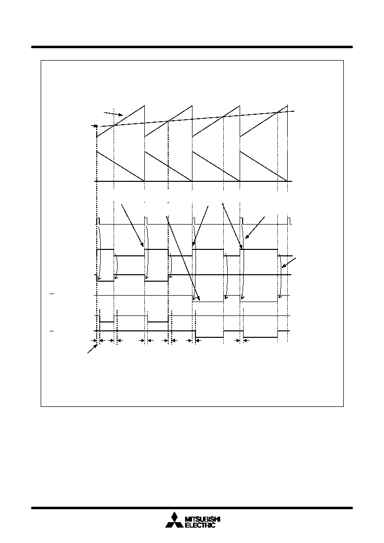
Mitsubishi microcomputers
M16C / 62A Group
SINGLE-CHIP 16-BIT CMOS MICROCOMPUTER
Timers' functions for three-phase motor control
106
Timer B2
Timer A4 output
U phase
U phase
Dead time
Carrier wave
Signal wave
A carrier wave of sawtooth waveform
m
n
p
Note: Set to sawtooth modulation mode and to three-phase mode 0.
U phase
output signal
U phase
output signal
The three-phase
shift register shifts
in synchronization
with the falling
edge of timer A4.
Trigger signal for
timer Ai start
(timer B2 overflow
signal)
Interrupt occurs.
Rewriting the value of timer A4.
Rewriting three-phase
output buffer register
Data transfer is made from the three-
phase buffer register to the three-
phase shift register in step with the
timing of the timer B overflow.
Interrupt occurs.
Rewriting the value of timer A4.
o
Figure 1.15.9. Timing chart of operation (4)
Mitsubishi microcomputers
M16C / 62A Group
SINGLE-CHIP 16-BIT CMOS MICROCOMPUTER
Serial I/O
107
Serial I/O
Serial I/O is configured as five channels: UART0, UART1, UART2, S I/O3 and S I/O4.
UART0 to 2
UART0, UART1 and UART2 each have an exclusive timer to generate a transfer clock, so they operate
independently of each other.
Figure 1.16.1 shows the block diagram of UART0, UART1 and UART2. Figures 1.16.2 and 1.16.3 show
the block diagram of the transmit/receive unit.
UARTi (i = 0 to 2) has two operation modes: a clock synchronous serial I/O mode and a clock asynchronous
serial I/O mode (UART mode). The contents of the serial I/O mode select bits (bits 0 to 2 at addresses
03A0
16
, 03A8
16
and 0378
16
) determine whether UARTi is used as a clock synchronous serial I/O or as a
UART. Although a few functions are different, UART0, UART1 and UART2 have almost the same functions.
UART2, in particular, is used for the SIM interface with some extra settings added in clock-asynchronous
serial I/O mode (Note). It also has the bus collision detection function that generates an interrupt request if
the TxD pin and the RxD pin are different in level.
Table 1.16.1 shows the comparison of functions of UART0 through UART2, and Figures 1.16.4 to 1.16.9
show the registers related to UARTi.
Note: SIM : Subscriber Identity Module
Note 1: Only when clock synchronous serial I/O mode.
Note 2: Only when clock synchronous serial I/O mode and 8-bit UART mode.
Note 3: Only when UART mode.
Note 4: Using for SIM interface.
UART0
UART1
UART2
Function
CLK polarity selection
Continuous receive mode selection
LSB first / MSB first selection
Impossible
Transfer clock output from multiple
pins selection
Impossible
Impossible
Serial data logic switch
Impossible
Sleep mode selection
Impossible
Impossible
TxD, RxD I/O polarity switch
Impossible
Possible
CMOS output
TxD, RxD port output format
CMOS output
N-channel open-drain
output
Impossible
Parity error signal output
Impossible
Impossible
Bus collision detection
Impossible
Possible
Possible
(Note 1)
Possible
(Note 1)
Possible
(Note 1)
Possible
(Note 3)
Possible
(Note 1)
Possible
(Note 1)
Possible
(Note 1)
Possible
(Note 1)
Possible
(Note 3)
Possible
(Note 1)
Possible
(Note 2)
Possible
(Note 1)
Possible
(Note 4)
Possible
(Note 4)
Table 1.16.1. Comparison of functions of UART0 through UART2
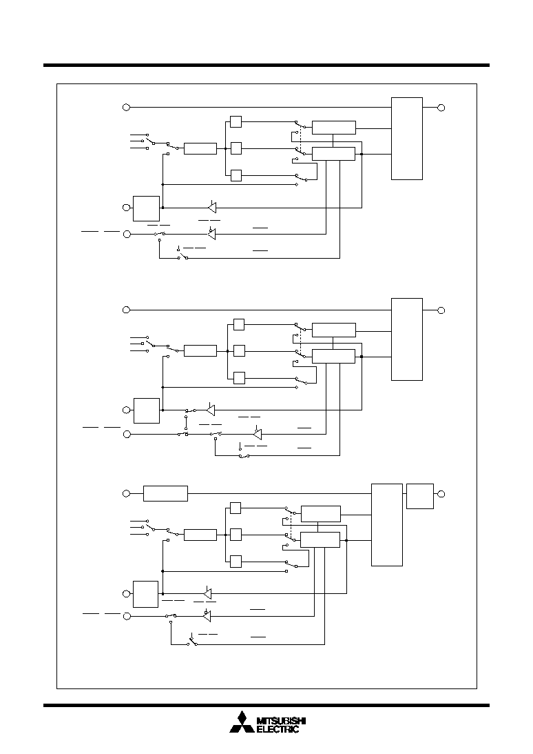
Mitsubishi microcomputers
M16C / 62A Group
SINGLE-CHIP 16-BIT CMOS MICROCOMPUTER
Serial I/O
108
Figure 1.16.1. Block diagram of UARTi (i = 0 to 2)
n0 : Values set to UART0 bit rate generator (U0BRG)
n1 : Values set to UART1 bit rate generator (U1BRG)
n2 : Values set to UART2 bit rate generator (U2BRG)
RxD
2
Reception
control circuit
Transmission
control circuit
1 / (n
2
+1)
1/16
1/16
1/2
Bit rate generator
(address 0379
16
)
Clock synchronous type
(when internal clock is selected)
UART reception
Clock synchronous type
UART transmission
Clock synchronous type
Clock synchronous type
(when internal clock is selected)
Clock synchronous type
(when external clock is
selected)
Receive
clock
Transmit
clock
CLK
2
CTS
2
/ RTS
2
f
1
f
8
f
32
Vcc
RTS
2
CTS
2
TxD
2
(UART2)
RxD polarity
reversing circuit
TxD
polarity
reversing
circuit
RxD
0
1 / (n
0
+1)
1/2
Bit rate generator
(address 03A1
16
)
Clock synchronous type
(when internal clock is selected)
UART reception
Clock synchronous type
UART transmission
Clock synchronous type
Clock synchronous type
(when internal clock is selected)
Clock synchronous type
(when external clock is
selected)
Receive
clock
Transmit
clock
CLK
0
Clock source selection
CTS
0
/ RTS
0
f
1
f
8
f
32
Reception
control circuit
Transmission
control circuit
Internal
External
Vcc
RTS
0
CTS
0
TxD
0
Transmit/
receive
unit
RxD
1
1 / (n
1
+1)
1/16
1/16
1/2
Bit rate generator
(address 03A9
16
)
Clock synchronous type
(when internal clock is selected)
UART reception
Clock synchronous type
UART transmission
Clock synchronous type
Clock synchronous type
(when internal clock is selected)
Clock synchronous type
(when external clock is
selected)
Receive
clock
Transmit
clock
CLK
1
Clock source selection
f
1
f
8
f
32
Reception
control circuit
Transmission
control circuit
Internal
External
RTS
1
CTS
1
TxD
1
(UART1)
(UART0)
CLK
polarity
reversing
circuit
CLK
polarity
reversing
circuit
CTS/RTS disabled
Clock output pin
select switch
CTS
1
/ RTS
1
/
CLKS
1
CTS/RTS disabled
CTS/RTS selected
CTS/RTS disabled
V
CC
CTS/RTS disabled
CTS/RTS selected
CTS/RTS disabled
CTS/RTS disabled
CTS/RTS
selected
CLK
polarity
reversing
circuit
Internal
External
Clock source selection
Transmit/
receive
unit
Transmit/
receive
unit
1/16
1/16
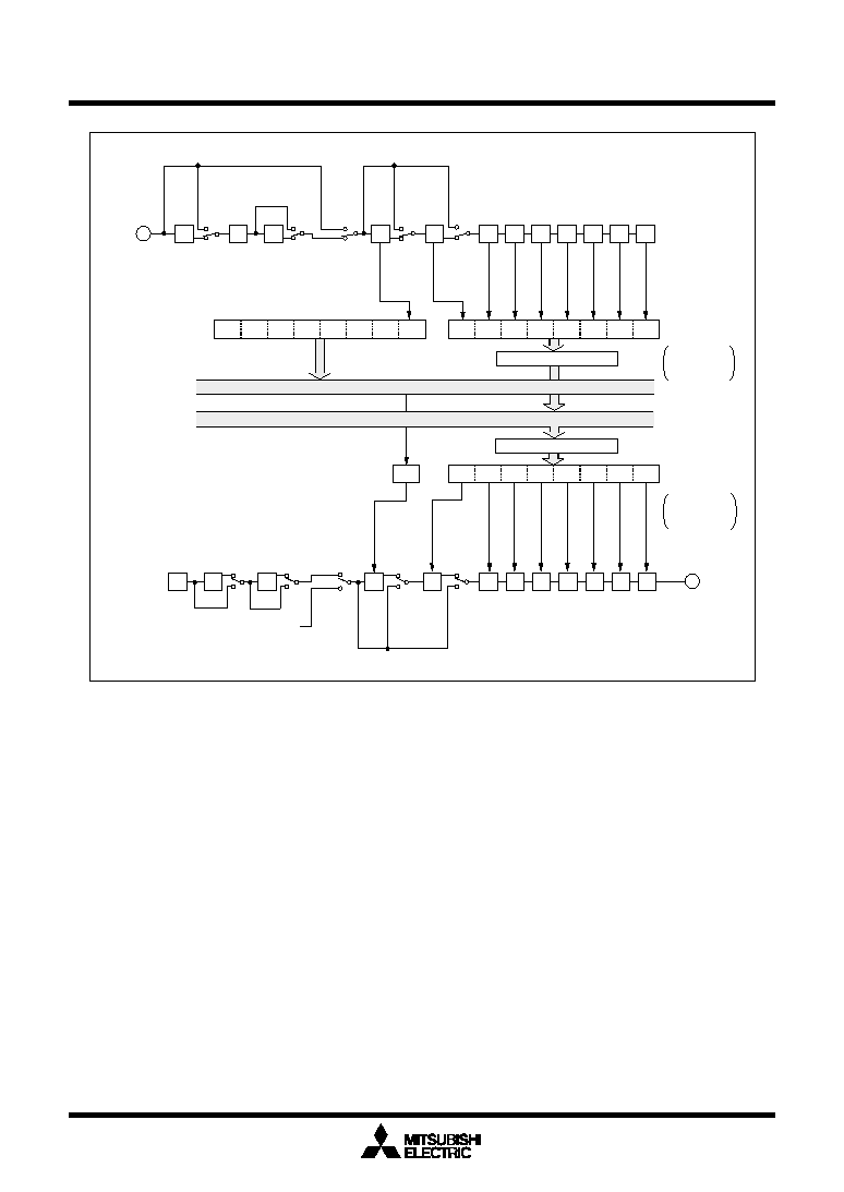
Mitsubishi microcomputers
M16C / 62A Group
SINGLE-CHIP 16-BIT CMOS MICROCOMPUTER
Serial I/O
109
Figure 1.16.2. Block diagram of UARTi (i = 0, 1) transmit/receive unit
SP
SP
PAR
2SP
1SP
UART
UART (7 bits)
UART (8 bits)
UART (7 bits)
UART (9 bits)
Clock
synchronous
type
Clock synchronous
type
TxDi
UARTi transmit register
PAR
enabled
PAR
disabled
D
8
D
7
D
6
D
5
D
4
D
3
D
2
D
1
D
0
SP: Stop bit
PAR: Parity bit
UARTi transmit
buffer register
MSB/LSB conversion circuit
UART (8 bits)
UART (9 bits)
Clock synchronous
type
UARTi receive
buffer register
UARTi receive register
2SP
1SP
PAR
enabled
PAR
disabled
UART
UART (7 bits)
UART (9 bits)
Clock
synchronous
type
Clock
synchronous type
UART (7 bits)
UART (8 bits)
RxDi
Clock
synchronous type
UART (8 bits)
UART (9 bits)
Address 03A6
16
Address 03A7
16
Address 03AE
16
Address 03AF
16
Address 03A2
16
Address 03A3
16
Address 03AA
16
Address 03AB
16
Data bus low-order bits
MSB/LSB conversion circuit
D
7
D
6
D
5
D
4
D
3
D
2
D
1
D
0
D
8
0
0
0
0
0
0
0
SP
SP
PAR
"0"
Data bus high-order bits
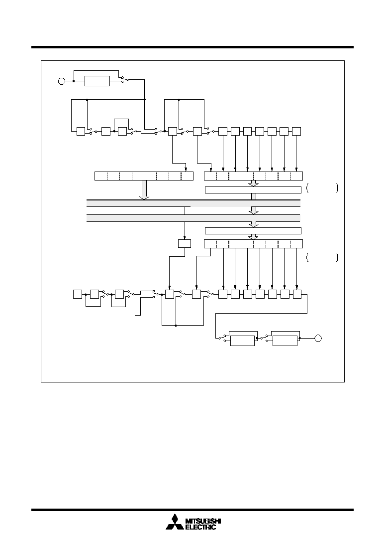
Mitsubishi microcomputers
M16C / 62A Group
SINGLE-CHIP 16-BIT CMOS MICROCOMPUTER
Serial I/O
110
SP
SP
PAR
2SP
1SP
UART
UART
(7 bits)
UART
(8 bits)
UART(7 bits)
UART
(9 bits)
Clock
synchronous
type
Clock
synchronous type
Data bus low-order bits
TxD2
UART2 transmit register
PAR
disabled
PAR
enabled
D
8
D
7
D
6
D
5
D
4
D
3
D
2
D
1
D
0
UART2 transmit
buffer register
UART
(8 bits)
UART
(9 bits)
Clock
synchronous type
UART2 receive
buffer register
UART2 receive register
2SP
1SP
UART
(7 bits)
UART
(8 bits)
UART(7 bits)
UART
(9 bits)
Clock
synchronous type
Clock
synchronous type
RxD2
UART
(8 bits)
UART
(9 bits)
Address 037E
16
Address 037F
16
Address 037A
16
Address 037B
16
Data bus high-order bits
D
7
D
6
D
5
D
4
D
3
D
2
D
1
D
0
D
8
0
0
0
0
0
0
0
SP
SP
PAR
"0"
Reverse
No reverse
Error signal
output circuit
RxD data
reverse circuit
Error signal output
enable
Error signal output
disable
Reverse
No reverse
Logic reverse circuit + MSB/LSB conversion circuit
Logic reverse circuit + MSB/LSB conversion circuit
PAR
enabled
PAR
disabled
UART
Clock
synchronous
type
TxD data
reverse circuit
SP: Stop bit
PAR: Parity bit
Figure 1.16.3. Block diagram of UART2 transmit/receive unit

Mitsubishi microcomputers
M16C / 62A Group
SINGLE-CHIP 16-BIT CMOS MICROCOMPUTER
Serial I/O
111
Figure 1.16.4. Serial I/O-related registers (1)
b7
UARTi bit rate generator (Note 1, 2)
b0
Symbol
Address
When reset
U0BRG
03A1
16
Indeterminate
U1BRG
03A9
16
Indeterminate
U2BRG
0379
16
Indeterminate
Function
Assuming that set value = n, BRGi divides the count source by
n + 1
00
16
to FF
16
Values that can be set
W
R
b7
b0
(b15)
(b8)
b7
b0
UARTi transmit buffer register (Note)
Function
Transmit data
Nothing is assigned.
In an attempt to write to these bits, write "0". The value, if read, turns out to be indeterminate.
Symbol
Address
When reset
U0TB
03A3
16
, 03A2
16
Indeterminate
U1TB
03AB
16
, 03AA
16
Indeterminate
U2TB
037B
16
, 037A
16
Indeterminate
W
R
(b15)
Symbol
Address
When reset
U0RB
03A7
16
, 03A6
16
Indeterminate
U1RB
03AF
16
, 03AE
16
Indeterminate
U2RB
037F
16
, 037E
16
Indeterminate
b7
b0
(b8)
b7
b0
UARTi receive buffer register
Function
(During UART mode)
Function
(During clock synchronous
serial I/O mode)
Bit name
Bit
symbol
0 : No framing error
1 : Framing error found
0 : No parity error
1 : Parity error found
0 : No error
1 : Error found
Note 1: Bits 15 through 12 are set to "0" when the serial I/O mode select bit (bits 2 to 0 at addresses 03A0
16
,
03A8
16
and 0378
16
) are set to "000
2
" or the receive enable bit is set to "0".
(Bit 15 is set to "0" when bits 14 to 12 all are set to "0".) Bits 14 and 13 are also set to "0" when the
lower byte of the UARTi receive buffer register (addresses 03A6
16
, 03AE
16
and 037E
16
) is read out.
Note 2: Arbitration lost detecting flag is allocated to U2RB and noting but "0" may be written. Nothing is
assigned in bit 11 of U0RB and U1RB. When write, set "0". The value, if read, turns out to be "0".
Invalid
Invalid
Invalid
OER
FER
PER
SUM
Overrun error flag (Note 1)
Framing error flag (Note 1)
Parity error flag (Note 1)
Error sum flag (Note 1)
0 : No overrun error
1 : Overrun error found
0 : No overrun error
1 : Overrun error found
Nothing is assigned.
In an attempt to write to these bits, write "0". The value, if read, turns out to be "0".
Receive data
W
R
Receive data
ABT
Arbitration lost detecting
flag (Note 2)
Invalid
0 : Not detected
1 : Detected
Note 1: Write a value to this register while transmit/receive halts.
Note 2: Use MOV instruction to write to this register.
Note: Use MOV instruction to write to this register.
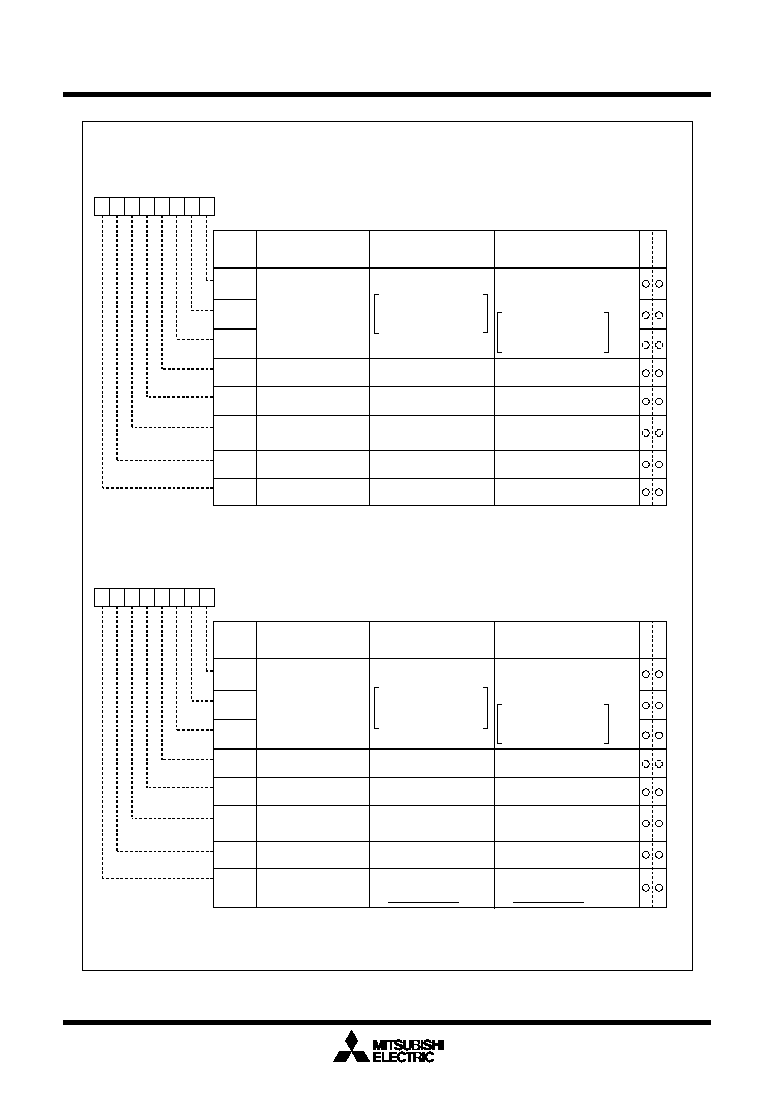
Mitsubishi microcomputers
M16C / 62A Group
SINGLE-CHIP 16-BIT CMOS MICROCOMPUTER
Serial I/O
112
UARTi transmit/receive mode register
Symbol
Address
When reset
UiMR(i=0,1)
03A0
16
, 03A8
16
00
16
b7
b6
b5
b4
b3
b2
b1
b0
Bit name
Bit
symbol
W
R
Must be fixed to 001
0 0 0 : Serial I/O invalid
0 1 0 : Must not be set.
0 1 1 : Must not be set.
1 1 1 : Must not be set.
b2 b1 b0
CKDIR
SMD1
SMD0
Serial I/O mode select bit
SMD2
Internal/external clock
select bit
STPS
PRY
PRYE
SLEP
Parity enable bit
0 : Internal clock
1 : External clock (Note)
Stop bit length select bit
Odd/even parity select bit
Sleep select bit
0 : One stop bit
1 : Two stop bits
0 : Parity disabled
1 : Parity enabled
0 : Sleep mode deselected
1 : Sleep mode selected
1 0 0 : Transfer data 7 bits long
1 0 1 : Transfer data 8 bits long
1 1 0 : Transfer data 9 bits long
0 0 0 : Serial I/O invalid
0 1 0 : Must not be set.
0 1 1 : Must not be set.
1 1 1 : Must not be set.
b2 b1 b0
0 : Internal clock
1 : External clock (Note)
Invalid
Valid when bit 6 = "1"
0 : Odd parity
1 : Even parity
Invalid
Invalid
Must always be "0"
Function
(During UART mode)
Function
(During clock synchronous
serial I/O mode)
UART2 transmit/receive mode register
Symbol
Address
When reset
U2MR
0378
16
00
16
b7
b6
b5
b4
b3
b2
b1
b0
Bit name
Bit
symbol
W
R
Must be fixed to 001
0 0 0 : Serial I/O invalid
0 1 0 : (Note 1)
0 1 1 : Must not be set.
1 1 1 : Must not be set.
b2 b1 b0
CKDIR
SMD1
SMD0
Serial I/O mode select bit
SMD2
Internal/external clock
select bit
STPS
PRY
PRYE
IOPOL
Parity enable bit
0 : Internal clock
1 : External clock (Note 2)
Stop bit length select bit
Odd/even parity select bit
TxD, RxD I/O polarity
reverse bit
0 : One stop bit
1 : Two stop bits
0 : Parity disabled
1 : Parity enabled
0 : No reverse
1 : Reverse
Usually set to "0"
1 0 0 : Transfer data 7 bits long
1 0 1 : Transfer data 8 bits long
1 1 0 : Transfer data 9 bits long
0 0 0 : Serial I/O invalid
0 1 0 : Must not be set.
0 1 1 : Must not be set.
1 1 1 : Must not be set.
b2 b1 b0
Invalid
Valid when bit 6 = "1"
0 : Odd parity
1 : Even parity
Invalid
Invalid
0 : No reverse
1 : Reverse
Usually set to "0"
Function
(During UART mode)
Function
(During clock synchronous
serial I/O mode)
Note 1: Bit 2 to bit 0 are set to "010
2
" when I
2
C mode is used.
Note 2: Set the corresponding port direction register to "0".
Must always be fixed to "0"
Note : Set the corresponding port direction register to "0".
Figure 1.16.5. Serial I/O-related registers (2)

Mitsubishi microcomputers
M16C / 62A Group
SINGLE-CHIP 16-BIT CMOS MICROCOMPUTER
Serial I/O
113
UARTi transmit/receive control register 0
Symbol
Address
When reset
UiC0(i=0,1)
03A4
16
, 03AC
16
08
16
b7
b6
b5
b4
b3
b2
b1
b0
Function
(During UART mode)
W
R
Function
(During clock synchronous
serial I/O mode)
TXEPT
CLK1
CLK0
CRS
CRD
NCH
CKPOL
BRG count source
select bit
Transmit register empty
flag
0 : Transmit data is output at
falling edge of transfer clock
and receive data is input at
rising edge
1 : Transmit data is output at
rising edge of transfer clock
and receive data is input at
falling edge
CLK polarity select bit
CTS/RTS function
select bit
CTS/RTS disable bit
Data output select bit
0 0 : f
1
is selected
0 1 : f
8
is selected
1 0 : f
32
is selected
1 1 : Must not be set.
b1 b0
0 : LSB first
1 : MSB first
0 : Data present in transmit
register (during transmission)
1 : No data present in transmit
register (transmission
completed)
0 : CTS/RTS function enabled
1 : CTS/RTS function disabled
(P6
0
and P6
4
function as
programmable I/O port)
0 : T
X
Di pin is CMOS output
1 : T
X
Di pin is N-channel
open-drain output
UFORM Transfer format select bit
0 0 : f
1
is selected
0 1 : f
8
is selected
1 0 : f
32
is selected
1 1 : Must not be set.
b1 b0
Valid when bit 4 = "0"
0 : CTS function is selected (Note 1)
1 : RTS function is selected (Note 2)
Valid when bit 4 = "0"
0 : CTS function is selected (Note 1)
1 : RTS function is selected (Note 2)
0 : Data present in transmit register
(during transmission)
1 : No data present in transmit
register (transmission completed)
0: T
X
Di pin is CMOS output
1: T
X
Di pin is N-channel
open-drain output
Must always be "0"
Bit name
Bit
symbol
Must always be "0"
Note 1: Set the corresponding port direction register to "0".
Note 2: The settings of the corresponding port register and port direction register are invalid.
0 : CTS/RTS function enabled
1 : CTS/RTS function disabled
(P6
0
and P6
4
function as
programmable I/O port)
UART2 transmit/receive control register 0
Symbol
Address
When reset
U2C0
037C
16
08
16
b7
b6
b5
b4
b3
b2
b1
b0
Function
(During UART mode)
W
R
Function
(During clock synchronous
serial I/O mode)
TXEPT
CLK1
CLK0
CRS
CRD
CKPOL
BRG count source
select bit
Transmit register empty
flag
0 : Transmit data is output at
falling edge of transfer clock
and receive data is input at
rising edge
1 : Transmit data is output at
rising edge of transfer clock
and receive data is input at
falling edge
CLK polarity select bit
CTS/RTS function
select bit
CTS/RTS disable bit
0 0 : f
1
is selected
0 1 : f
8
is selected
1 0 : f
32
is selected
1 1 : Must not be set.
b1 b0
0 : LSB first
1 : MSB first
0 : Data present in transmit
register (during transmission)
1 : No data present in transmit
register (transmission
completed)
0 : CTS/RTS function enabled
1 : CTS/RTS function disabled
(P7
3
functions
programmable I/O port)
0 : TXDi pin is CMOS output
1 : TXDi pin is N-channel
open-drain output
UFORM Transfer format select bit
(Note 3)
0 0 : f
1
is selected
0 1 : f
8
is selected
1 0 : f
32
is selected
1 1 : Must not be set.
b1 b0
Valid when bit 4 = "0"
0 : CTS function is selected (Note 1)
1 : RTS function is selected (Note 2)
Valid when bit 4 = "0"
0 : CTS function is selected (Note 1)
1 : RTS function is selected (Note 2)
0 : Data present in transmit register
(during transmission)
1 : No data present in transmit
register (transmission completed)
0: TXDi pin is CMOS output
1: TXDi pin is N-channel
open-drain output
Must always be "0"
Bit name
Bit
symbol
Note 1: Set the corresponding port direction register to "0".
Note 2: The settings of the corresponding port register and port direction register are invalid.
Note 3: Only clock synchronous serial I/O mode and 8-bit UART mode are valid.
0 : CTS/RTS function enabled
1 : CTS/RTS function disabled
(P7
3
functions programmable
I/O port)
Nothing is assigned.
In an attempt to write to this bit, write "0". The value, if read, turns out to be "0".
0 : LSB first
1 : MSB first
Figure 1.16.6. Serial I/O-related registers (3)

Mitsubishi microcomputers
M16C / 62A Group
SINGLE-CHIP 16-BIT CMOS MICROCOMPUTER
Serial I/O
114
Figure 1.16.7. Serial I/O-related registers (4)
UARTi transmit/receive control register 1
Symbol
Address
When reset
UiC1(i=0,1)
03A5
16
,
03AD
16
02
16
b7
b6
b5
b4
b3
b2
b1
b0
Bit name
Bit
symbol
W
R
Function
(During UART mode)
Function
(During clock synchronous
serial I/O mode)
TE
TI
RE
RI
Transmit enable bit
Receive enable bit
Receive complete flag
Transmit buffer
empty flag
0 : Transmission disabled
1 : Transmission enabled
0 : Data present in
transmit buffer register
1 : No data present in
transmit buffer register
0 : Reception disabled
1 : Reception enabled
0 : Transmission disabled
1 : Transmission enabled
0 : Data present in
transmit buffer register
1 : No data present in
transmit buffer register
0 : Reception disabled
1 : Reception enabled
0 : No data present in
receive buffer register
1 : Data present in
receive buffer register
0 : No data present in
receive buffer register
1 : Data present in
receive buffer register
Nothing is assigned.
In an attempt to write to these bits, write "0". The value, if read, turns out to be "0".
UART2 transmit/receive control register 1
Symbol
Address
When reset
U2C1
037D
16
02
16
b7
b6
b5
b4
b3
b2
b1
b0
Bit name
Bit
symbol
W
R
Function
(During UART mode)
Function
(During clock synchronous
serial I/O mode)
TE
TI
RE
RI
Transmit enable bit
Receive enable bit
Receive complete flag
Transmit buffer
empty flag
0 : Transmission disabled
1 : Transmission enabled
0 : Data present in
transmit buffer register
1 : No data present in
transmit buffer register
0 : Reception disabled
1 : Reception enabled
0 : Transmission disabled
1 : Transmission enabled
0 : Data present in
transmit buffer register
1 : No data present in
transmit buffer register
0 : Reception disabled
1 : Reception enabled
0 : No data present in
receive buffer register
1 : Data present in
receive buffer register
0 : No data present in
receive buffer register
1 : Data present in
receive buffer register
U2IRS
UART2 transmit interrupt
cause select bit
0 : Transmit buffer empty
(TI = 1)
1 : Transmit is completed
(TXEPT = 1)
0 : Transmit buffer empty
(TI = 1)
1 : Transmit is completed
(TXEPT = 1)
U2RRM UART2 continuous
receive mode enable bit
0 : Continuous receive
mode disabled
1 : Continuous receive
mode enabled
Must always be "0"
Data logic select bit
0 : No reverse
1 : Reverse
0 : No reverse
1 : Reverse
U2LCH
U2ERE Error signal output
enable bit
Must be fixed to "0"
0 : Output disabled
1 : Output enabled

Mitsubishi microcomputers
M16C / 62A Group
SINGLE-CHIP 16-BIT CMOS MICROCOMPUTER
Serial I/O
115
Note: When using multiple pins to output the transfer clock, the following requirements must be met:
∑ UART1 internal/external clock select bit (bit 3 at address 03A8
16
) = "0".
UART transmit/receive control register 2
Symbol
Address
When reset
UCON
03B0
16
X0000000
2
b7
b6
b5
b4
b3
b2
b1
b0
Bit
name
Bit
symbol
W
R
Function
(During UART mode)
Function
(During clock synchronous
serial I/O mode)
CLKMD0
CLKMD1
Reserved bit
UART0 transmit
interrupt cause select bit
UART0 continuous
receive mode enable bit
0 : Continuous receive
mode disabled
1 : Continuous receive
mode enable
UART1 continuous
receive mode enable bit
CLK/CLKS select bit 0
UART1 transmit
interrupt cause select bit
0 :
Transmit buffer empty (Tl = 1)
1 : Transmission completed
(TXEPT = 1)
0 :
Transmit buffer empty (Tl = 1)
1 : Transmission completed
(TXEPT = 1)
0 : Normal mode
(CLK output is CLK1 only)
1 : Transfer clock output
from multiple pins
function selected
0 : Continuous receive
mode disabled
1 : Continuous receive
mode enabled
Nothing is assigned.
In an attempt to write to this bit, write "0". The value, if read, turns out to be indeterminate.
0 : Transmit buffer empty (Tl = 1)
1 : Transmission completed
(TXEPT = 1)
0 : Transmit buffer empty (Tl = 1)
1 : Transmission completed
(TXEPT = 1)
Must always be "0"
U0IRS
U1IRS
U0RRM
U1RRM
Invalid
CLK/CLKS select
bit 1 (Note)
Valid when bit 5 = "1"
0 : Clock output to CLK1
1 : Clock output to CLKS1
UART2 special mode register
Symbol
Address
When reset
U2SMR
0377
16
00
16
b7 b6
b5
b4
b3
b2
b1 b0
Bit
name
Bit
symbol
W
R
Function
(During UART mode)
Function
(During clock synchronous
serial I/O mode)
ABSCS
ACSE
SSS
I
2
C mode select bit
Bus busy flag
0 : STOP condition detected
1 : START condition detected
SCLL sync output
enable bit
Bus collision detect
sampling
clock select bit
Arbitration lost detecting
flag control bit
0 : Normal mode
1 : I
2
C mode
0 : Update per bit
1 : Update per byte
IICM
ABC
BBS
LSYN
0 : Ordinary
1 : Falling edge of R
X
D
2
0 : Disabled
1 : Enabled
Transmit start condition
select bit
Must always be "0"
0 : Rising edge of transfer
clock
1 : Underflow signal of timer A0
Auto clear function
select bit of transmit
enable bit
0 : No auto clear function
1 : Auto clear at occurrence of
bus collision
Must always be "0"
Must always be "0"
Must always be "0"
Must always be "0"
Must always be "0"
Must always be "0"
Note 1: Nothing but "0" may be written.
Note 2: When not in I
2
C mode, do not set this bit by writing a "1". During normal mode, fix it to "0". When this
bit = "0", UART2 special mode register 3 (U2SMR3 at address 0375
16
) bits 7 to 5 (DL2 to DL0 = SDA
digital delay setup bits) are initialized to "000", with the analog delay circuit selected. Also, when SDDS
= "0", the U2SMR3 register cannot be read or written to.
Note 3: When analog delay is selected, only the analog delay value is effective; when digital delay is selected,
only the digital delay value is effective.
(Note1)
SDDS
SDA digital delay select
bit (Note 2, Note 3)
Must always be "0"
0 : Analog delay output
is selected
1 : Digital delay output
is selected
(must always be "0" when
not using I C mode)
2
Must always be set to
"0"
0
Must always be "0"
Must always be "0"
Figure 1.16.8. Serial I/O-related registers (5)

Mitsubishi microcomputers
M16C / 62A Group
SINGLE-CHIP 16-BIT CMOS MICROCOMPUTER
Serial I/O
116
Figure 1.16.9. Serial I/O-related registers (6)
UART2 special mode register 2 (I C bus exclusive use register)
Symbol
Address
When reset
U2SMR2
0376
16
00
16
b7
b6 b5
b4
b3
b2
b1
b0
Bit name
Bit
symbol
W
R
Function
(I2C bus exclusive use)
STAC
SWC2
SDHI
I C mode select bit 2
SCL wait output bit
0 : Disabled
1 : Enabled
SDA output stop bit
UART2 initialization bit
Clock-synchronous bit
Refer to Table 1.16.11
0 : Disabled
1 : Enabled
IICM2
CSC
SWC
ALS
0 : Disabled
1 : Enabled
SDA output disable bit
SCL wait output bit 2
0: Enabled
1: Disabled (high impedance)
0 : Disabled
1 : Enabled
0: UART2 clock
1: 0 output
2
SHTC
Start/stop condition
control bit
Set this bit to "1" in I
2
C mode
(refer to Table 1.16.12)
2
UART2 special mode register 3 (I C bus exclusive use register)
Symbol
Address
When reset
U2SMR3
0375
16
Indeterminate
(However, when SDDS = "1", the initial value is "00
16
")
b7
b6 b5
b4
b3
b2
b1
b0
Bit name
Bit
symbol
W
R
Function
(I C bus exclusive use register)
DL2
SDA digital delay setup
bit
(Note 1, Note 2, Note 3,
Note 4)
DL0
DL1
0 0 0 : Analog delay is selected
0 0 1 : 1 to 2 cycle(s) of 1/f(X
IN
)
0 1 0 : 2 to 3 cycles of 1/f(X
IN
)
0 1 1 : 3 to 4 cycles of 1/f(X
IN
)
1 0 0 : 4 to 5 cycles of 1/f(X
IN
)
1 0 1 : 5 to 6 cycles of 1/f(X
IN
)
1 1 0 : 6 to 7 cycles of 1/f(X
IN
)
1 1 1 : 7 to 8 cycles of 1/f(X
IN
)
2
Nothing is assigned.
In an attempt to write to these bits, write "0". The value, if read, turns out to be
indeterminate. However, when SDDS = "1", the value "0" is read out (Note 1)
2
b7 b6 b5
Note 1: This bit can be read or written to when UART2 special mode register (U2SMR at address 0377
16
) bit
7 (SDDS: SDA digital delay select bit) = "1". When the initial value of UART2 special mode register 3
(U2SMR3) is read after setting SDDS = "1", the value is "00
16
". When writing to UART2 special mode
register 3 (U2SMR3) after setting SDDS = "1", be sure to write 0's to bits 0≠4. When SDDS = "0",
this register cannot be written to; when read, the value is indeterminate.
Note 2: These bits are initialized to "000" when SDDS = "0", with the analog delay circuit selected. After a reset,
these bits are set to "000", with the analog delay circuit selected. However, because these bits can be
read only when SDDS = "1", the value read from these bits when SDDS = "0" is indeterminate.
Note 3: When analog delay is selected, only the analog delay value is effective; when digital delay is selected,
only the digital delay value is effective.
Note 4: The amount of delay varies with the load on SCL and SDA pins. Also, when using an external clock, the
amount of delay increases by about 100 ns, so be sure to take this into account when using the device.
Digital delay
is selected

Mitsubishi microcomputers
M16C / 62A Group
SINGLE-CHIP 16-BIT CMOS MICROCOMPUTER
Clock synchronous serial I/O mode
117
(1) Clock synchronous serial I/O mode
The clock synchronous serial I/O mode uses a transfer clock to transmit and receive data. Tables 1.16.2
and 1.16.3 list the specifications of the clock synchronous serial I/O mode. Figure 1.16.10 shows the
UARTi transmit/receive mode register.
Table 1.16.2. Specifications of clock synchronous serial I/O mode (1)
Item
Specification
Transfer data format
∑ Transfer data length: 8 bits
Transfer clock
∑ When internal clock is selected (bit 3 at addresses 03A0
16
, 03A8
16
, 0378
16
= "0") : fi/ 2(n+1)
(Note 1) fi = f
1
, f
8
, f
32
∑ When external clock is selected (bit 3 at addresses 03A0
16
, 03A8
16
, 0378
16
= "1") : Input from CLKi pin
Transmission/reception control
_______
_______
_______
_______
∑
CTS
function,
RTS
function,
CTS
and
RTS
function invalid: selectable
Transmission start condition
∑ To start transmission, the following requirements must be met:
_
Transmit enable bit (bit 0 at addresses 03A5
16
, 03AD
16
, 037D
16
) = "1"
_
Transmit buffer empty flag (bit 1 at addresses 03A5
16
, 03AD
16
, 037D
16
) = "0"
_______
_______
_
When CTS function selected, CTS input level = "L"
∑ Furthermore, if external clock is selected, the following requirements must also be met:
_
CLKi polarity select bit (bit 6 at addresses 03A4
16
, 03AC
16
, 037C
16
) = "0":
CLKi input level = "H"
_
CLKi polarity select bit (bit 6 at addresses 03A4
16
, 03AC
16
, 037C
16
) = "1":
CLKi input level = "L"
Reception start condition
∑ To start reception, the following requirements must be met:
_
Receive enable bit (bit 2 at addresses 03A5
16
, 03AD
16
, 037D
16
) = "1"
_
Transmit enable bit (bit 0 at addresses 03A5
16
, 03AD
16
, 037D
16
) = "1"
_
Transmit buffer empty flag (bit 1 at addresses 03A5
16
, 03AD
16
, 037D
16
) = "0"
∑ Furthermore, if external clock is selected, the following requirements must
also be met:
_
CLKi polarity select bit (bit 6 at addresses 03A4
16
, 03AC
16
, 037C
16
) = "0":
CLKi input level = "H"
_
CLKi polarity select bit (bit 6 at addresses 03A4
16
, 03AC
16
, 037C
16
) = "1":
CLKi input level = "L"
∑ When transmitting
_
Transmit interrupt cause select bit (bits 0, 1 at address 03B0
16
, bit 4 at
address 037D
16
) = "0": Interrupts requested when data transfer from UARTi
transfer buffer register to UARTi transmit register is completed
_
Transmit interrupt cause select bit (bits 0, 1 at address 03B0
16
, bit 4 at
address 037D
16
) = "1": Interrupts requested when data transmission from
UARTi transfer register is completed
∑ When receiving
_
Interrupts requested when data transfer from UARTi receive register to
UARTi receive buffer register is completed
Error detection
∑ Overrun error (Note 2)
This error occurs when the next data is ready before contents of UARTi
receive buffer register are read out
Interrupt request
generation timing
Note 1: "n" denotes the value 00
16
to FF
16
that is set to the UART bit rate generator.
Note 2: If an overrun error occurs, the UARTi receive buffer will have the next data written in. Note also that
the UARTi receive interrupt request bit does not change.

Mitsubishi microcomputers
M16C / 62A Group
SINGLE-CHIP 16-BIT CMOS MICROCOMPUTER
Clock synchronous serial I/O mode
118
Item
Specification
Select function
∑ CLK polarity selection
Whether transmit data is output/input timing at the rising edge or falling edge
of the transfer clock can be selected
∑ LSB first/MSB first selection
Whether transmission/reception begins with bit 0 or bit 7 can be selected
∑ Continuous receive mode selection
Reception is enabled simultaneously by a read from the receive buffer register
∑ Transfer clock output from multiple pins selection (UART1)
UART1 transfer clock can be chosen by software to be output from one of
the two pins set
∑ Switching serial data logic (UART2)
Whether to reverse data in writing to the transmission buffer register or
reading the reception buffer register can be selected.
∑ TxD, RxD I/O polarity reverse (UART2)
This function is reversing TxD port output and RxD port input. All I/O data
level is reversed.
Table 1.16.3. Specifications of clock synchronous serial I/O mode (2)

Mitsubishi microcomputers
M16C / 62A Group
SINGLE-CHIP 16-BIT CMOS MICROCOMPUTER
Clock synchronous serial I/O mode
119
Figure 1.16.10. UARTi transmit/receive mode register in clock synchronous serial I/O mode
Symbol
Address
When reset
UiMR(i=0,1)
03A0
16
, 03A8
16
00
16
CKDIR
UARTi transmit/receive mode registers
Internal/external clock
select bit
STPS
PRY
PRYE
SLEP
0 : Internal clock
1 : External clock (Note)
Bit name
Function
Bit symbol
W
R
b7
b6
b5
b4
b3
b2
b1
b0
0 (Must always be "0" in clock synchronous serial I/O mode)
0 1
0
SMD0
SMD1
SMD2
Serial I/O mode select bit
0 0 1 : Clock synchronous serial
I/O mode
b2 b1 b0
0
Invalid in clock synchronous serial I/O mode
Symbol
Address
When reset
U2MR
0378
16
00
16
CKDIR
UART2 transmit/receive mode register
Internal/external clock
select bit
STPS
PRY
PRYE
IOPOL
0 : Internal clock
1 : External clock (Note 2)
Bit name
Function
Bit symbol
W
R
b7
b6
b5
b4
b3
b2
b1
b0
0 1
0
SMD0
SMD1
SMD2
Serial I/O mode select bit
0 0 1 : Clock synchronous serial
I/O mode
b2 b1 b0
0
Invalid in clock synchronous serial I/O mode
TxD, RxD I/O polarity
reverse bit (Note 1)
0 : No reverse
1 : Reverse
Note 1: Usually set to "0".
Note 2: Set the corresponding port direction register to "0".
Note : Set the corresponding port direction register to "0".

Mitsubishi microcomputers
M16C / 62A Group
SINGLE-CHIP 16-BIT CMOS MICROCOMPUTER
Clock synchronous serial I/O mode
120
Table 1.16.4 lists the functions of the input/output pins during clock synchronous serial I/O mode. This
table shows the pin functions when the transfer clock output from multiple pins function is not selected.
Note that for a period from when the UARTi operation mode is selected to when transfer starts, the TxDi
pin outputs an "H". (If the N-channel open-drain is selected, this pin is in floating state.)
Table 1.16.4. Input/output pin functions in clock synchronous serial I/O mode
Pin name
Function
Method of selection
TxDi
(P6
3
, P6
7
, P7
0
)
Serial data output
Serial data input
Transfer clock output
Transfer clock input
Programmable I/O port
(Outputs dummy data when performing reception only)
RxDi
(P6
2
, P6
6
, P7
1
)
CLKi
(P6
1
, P6
5
, P7
2
)
Internal/external clock select bit (bit 3 at address 03A0
16
, 03A8
16
, 0378
16
) = "0"
Internal/external clock select bit (bit 3 at address 03A0
16
, 03A8
16
, 0378
16
) = "1"
Port P6
1
, P6
5
and P7
2
direction register (bits 1 and 5 at address 03EE
16
,
bit 2 at address 03EF
16
) = "0"
Port P6
2
, P6
6
and P7
1
direction register (bits 2 and 6 at address 03EE
16
,
bit 1 at address 03EF
16
)= "0"
(Can be used as an input port when performing transmission only)
CTS/RTS disable bit (bit 4 at address 03A4
16
, 03AC
16
, 037C
16
) ="0"
CTS/RTS function select bit (bit 2 at address 03A4
16
, 03AC
16
, 037C
16
) = "0"
Port P6
0
, P6
4
and P7
3
direction register (bits 0 and 4 at address 03EE
16
,
bit 3 at address 03EF
16
) = "0"
CTS/RTS disable bit (bit 4 at address 03A4
16
, 03AC
16
, 037C
16)
= "0"
CTS/RTS function select bit (bit 2 at address 03A4
16
, 03AC
16
, 037C
16
) = "1"
CTS/RTS disable bit (bit 4 at address 03A4
16
, 03AC
16
, 037C
16
) = "1"
CTS input
RTS output
CTSi/RTSi
(P6
0
, P6
4
, P7
3
)
(when transfer clock output from multiple pins is not selected)

Mitsubishi microcomputers
M16C / 62A Group
SINGLE-CHIP 16-BIT CMOS MICROCOMPUTER
Clock synchronous serial I/O mode
121
Figure 1.16.11. Typical transmit/receive timings in clock synchronous serial I/O mode
∑ Example of transmit timing (when internal clock is selected)
D
0
D
1
D
2
D
3
D
4
D
5
D
6
D
7
D
0
D
1
D
2
D
3
D
4
D
5
D
6
D
7
D
0
D
1
D
2
D
3
D
4
D
5
D
6
D
7
Tc
T
CLK
Stopped pulsing because transfer enable bit = "0"
Data is set in UARTi transmit buffer register
Tc = TCLK = 2(n + 1) / fi
fi: frequency of BRGi count source (f
1
, f
8
, f
32
)
n: value set to BRGi
Transfer clock
Transmit enable
bit (TE)
Transmit buffer
empty flag (Tl)
CLKi
TxDi
Transmit
register empty
flag (TXEPT)
"H"
"L"
"0"
"1"
"0"
"1"
"0"
"1"
CTSi
The above timing applies to the following settings:
∑ Internal clock is selected.
∑ CTS function is selected.
∑ CLK polarity select bit = "0".
∑ Transmit interrupt cause select bit = "0".
Transmit interrupt
request bit (IR)
"0"
"1"
Stopped pulsing because CTS = "H"
Transferred from UARTi transmit buffer register to UARTi transmit register
Shown in ( ) are bit symbols.
Cleared to "0" when interrupt request is accepted, or cleared by software
1 / f
EXT
Dummy data is set in UARTi transmit buffer register
Transmit enable
bit (TE)
Transmit buffer
empty flag (Tl)
CLKi
RxDi
Receive complete
flag (Rl)
RTSi
"H"
"L"
"0"
"1"
"0"
"1"
"0"
"1"
Receive enable
bit (RE)
"0"
"1"
Receive data is taken in
Transferred from UARTi transmit buffer register to UARTi transmit register
Read out from UARTi receive buffer register
The above timing applies to the following settings:
∑ External clock is selected.
∑ RTS function is selected.
∑ CLK polarity select bit = "0".
f
EXT
: frequency of external clock
Transferred from UARTi receive register
to UARTi receive buffer register
Receive interrupt
request bit (IR)
"0"
"1"
D
0
D
1
D
2
D
3
D
4
D
5
D
6
D
7
D
0
D
1
D
2
D
3
D
4
D
5
Shown in ( ) are bit symbols.
Meet the following conditions are met when the CLK
input before data reception = "H"
∑ Transmit enable bit "1"
∑ Receive enable bit "1"
∑ Dummy data write to UARTi transmit buffer register
Cleared to "0" when interrupt request is accepted, or cleared by software
∑ Example of receive timing (when external clock is selected)

Mitsubishi microcomputers
M16C / 62A Group
SINGLE-CHIP 16-BIT CMOS MICROCOMPUTER
Clock synchronous serial I/O mode
122
(a) Polarity select function
As shown in Figure 1.16.12, the CLK polarity select bit (bit 6 at addresses 03A4
16
, 03AC
16
, 037C
16
)
allows selection of the polarity of the transfer clock.
∑ When CLK polarity select bit = "1"
Note 2: The CLKi pin level when not
transferring data is "L".
D
1
D
2
D
3
D
4
D
5
D
6
D
7
D
1
D
2
D
3
D
4
D
5
D
6
D
7
D
0
D
0
T
X
D
i
R
X
D
i
CLK
i
∑ When CLK polarity select bit = "0"
Note 1: The CLKi pin level when not
transferring data is "H".
D
1
D
2
D
3
D
4
D
5
D
6
D
7
D0
D
1
D
2
D
3
D
4
D
5
D
6
D
7
D
0
T
X
D
i
R
X
D
i
CLK
i
Figure 1.16.12. Polarity of transfer clock
(b) LSB first/MSB first select function
As shown in Figure 1.16.13, when the transfer format select bit (bit 7 at addresses 03A4
16
, 03AC
16
,
037C
16
) = "0", the transfer format is "LSB first"; when the bit = "1", the transfer format is "MSB first".
Figure 1.16.13. Transfer format
LSB first
∑ When transfer format select bit = "0"
D0
D
0
D
1
D
2
D
3
D
4
D
5
D
6
D
7
D
1
D
2
D
3
D
4
D
5
D
6
D
7
T
X
D
i
R
X
D
i
CLK
i
∑ When transfer format select bit = "1"
D
6
D
5
D
4
D
3
D
2
D
1
D
0
D
7
D
7
D
6
D
5
D
4
D
3
D
2
D
1
D
0
T
X
D
i
R
X
D
i
CLK
i
MSB first
Note: This applies when the CLK polarity select bit = "0".

Mitsubishi microcomputers
M16C / 62A Group
SINGLE-CHIP 16-BIT CMOS MICROCOMPUTER
Clock synchronous serial I/O mode
123
(c) Transfer clock output from multiple pins function (UART1)
This function allows the setting two transfer clock output pins and choosing one of the two to output a
clock by using the CLK and CLKS select bit (bits 4 and 5 at address 03B0
16
). (See Figure 1.16.14.)
The multiple pins function is valid only when the internal clock is selected for UART1.
Figure 1.16.14. The transfer clock output from the multiple pins function usage
Microcomputer
T
X
D
1
(P6
7
)
CLKS
1
(P6
4
)
CLK
1
(P6
5
)
IN
CLK
IN
CLK
Note: This applies when the internal clock is selected and transmission
is performed only in clock synchronous serial I/O mode.
(d) Continuous receive mode
If the continuous receive mode enable bit (bits 2 and 3 at address 03B0
16
, bit 5 at address 037D
16
) is
set to "1", the unit is placed in continuous receive mode. In this mode, when the receive buffer register
is read out, the unit simultaneously goes to a receive enable state without having to set dummy data to
the transmit buffer register back again.
(e) Serial data logic switch function (UART2)
When the data logic select bit (bit6 at address 037D
16
) = "1", and writing to transmit buffer register or
reading from receive buffer register, data is reversed. Figure 1.16.15 shows the example of serial data
logic switch timing.
Figure 1.16.15. Serial data logic switch timing
D0
D1
D2
D3
D4
D5
D6
D7
D0
D1
D2
D3
D4
D5
D6
D7
Transfer clock
TxD
2
(no reverse)
TxD
2
(reverse)
"H"
"L"
"H"
"L"
"H"
"L"
∑When LSB first

Mitsubishi microcomputers
M16C / 62A Group
SINGLE-CHIP 16-BIT CMOS MICROCOMPUTER
Clock asynchronous serial I/O (UART) mode
124
Item
Specification
Transfer data format
∑ Character bit (transfer data): 7 bits, 8 bits, or 9 bits as selected
∑ Start bit: 1 bit
∑ Parity bit: Odd, even, or nothing as selected
∑ Stop bit: 1 bit or 2 bits as selected
Transfer clock
∑ When internal clock is selected (bit 3 at addresses 03A0
16
, 03A8
16
, 0378
16
= "0") :
fi/16(n+1) (Note 1)
fi = f
1
, f
8
, f
32
∑ When external clock is selected (bit 3 at addresses 03A0
16
, 03A8
16
="1") :
f
EXT
/16(n+1) (Note 1) (Note 2) (Do not set external clock for UART2)
Transmission/reception control
_______
_______
_______
_______
∑
CTS
function,
RTS
function,
CTS
and
RTS
function invalid: selectable
Transmission start condition
∑ To start transmission, the following requirements must be met:
- Transmit enable bit (bit 0 at addresses 03A5
16
, 03AD
16
, 037D
16
) = "1"
- Transmit buffer empty flag (bit 1 at addresses 03A5
16
, 03AD
16
, 037D
16
) = "0"
_______
_______
- When CTS function selected, CTS input level = "L"
Reception start condition
∑ To start reception, the following requirements must be met:
- Receive enable bit (bit 2 at addresses 03A5
16
, 03AD
16
, 037D
16
) = "1"
- Start bit detection
Interrupt request
∑ When transmitting
generation timing
-
T
ransmit interrupt cause select bits (bits 0,1 at address 03B0
16
, bit4 at
address 037D
16
) = "0": Interrupts requested when data transfer from UARTi
transfer buffer register to UARTi transmit register is completed
- Transmit interrupt cause select bits (bits 0, 1 at address 03B0
16
, bit4 at
address 037D
16
) = "1": Interrupts requested when data transmission from
UARTi transfer register is completed
∑
When receiving
- Interrupts requested when data transfer from UARTi receive register to
UARTi receive buffer register is completed
Error detection
∑ Overrun error (Note 3)
This error occurs when the next data is ready before contents of UARTi
receive buffer register are read out
∑ Framing error
This error occurs when the number of stop bits set is not detected
∑ Parity error
This error occurs when if parity is enabled, the number of 1's in parity and
character bits does not match the number of 1's set
∑ Error sum flag
This flag is set (= 1) when any of the overrun, framing, and parity errors is
encountered
(2) Clock asynchronous serial I/O (UART) mode
The UART mode allows transmitting and receiving data after setting the desired transfer rate and transfer
data format. Tables 1.16.5 and 1.16.6 list the specifications of the UART mode. Figure 1.16.16 shows
the UARTi transmit/receive mode register.
Table 1.16.5. Specifications of UART Mode (1)
Note 1: `n' denotes the value 00
16
to FF
16
that is set to the UARTi bit rate generator.
Note 2: f
EXT
is input from the CLKi pin.
Note 3: If an overrun error occurs, the UARTi receive buffer will have the next data written in. Note also that
the UARTi receive interrupt request bit is not set to "1".

Clock asynchronous serial I/O (UART) mode
Mitsubishi microcomputers
M16C / 62A Group
SINGLE-CHIP 16-BIT CMOS MICROCOMPUTER
125
Table 1.16.6. Specifications of UART Mode (2)
Item
Specification
Select function
∑ Sleep mode selection (UART0, UART1)
This mode is used to transfer data to and from one of multiple slave micro-
computers
∑ Serial data logic switch (UART2)
This function is reversing logic value of transferring data. Start bit, parity bit
and stop bit are not reversed.
∑ T
X
D, R
X
D I/O polarity switch (UART2)
This function is reversing T
X
D port output and R
X
D port input. All I/O data
level is reversed.

Mitsubishi microcomputers
M16C / 62A Group
SINGLE-CHIP 16-BIT CMOS MICROCOMPUTER
Clock asynchronous serial I/O (UART) mode
126
Figure 1.16.16. UARTi transmit/receive mode register in UART mode
Symbol
Address
When reset
UiMR(i=0,1)
03A0
16
, 03A8
16
00
16
CKDIR
UARTi transmit / receive mode registers
Internal / external clock
select bit
STPS
PRY
PRYE
SLEP
0 : Internal clock
1 : External clock (Note)
Bit name
Function
Bit symbol
W
R
b7
b6
b5
b4
b3
b2
b1
b0
SMD0
SMD1
SMD2
Serial I/O mode select bit
b2 b1 b0
0 : One stop bit
1 : Two stop bits
0 : Parity disabled
1 : Parity enabled
0 : Sleep mode deselected
1 : Sleep mode selected
1 0 0 : Transfer data 7 bits long
1 0 1 : Transfer data 8 bits long
1 1 0 : Transfer data 9 bits long
Valid when bit 6 = "1"
0 : Odd parity
1 : Even parity
Stop bit length select bit
Odd / even parity
select bit
Parity enable bit
Sleep select bit
Symbol
Address
When reset
U2MR
0378
16
00
16
CKDIR
UART2 transmit / receive mode register
Internal / external clock
select bit
STPS
PRY
PRYE
IOPOL
Must always be fixed to "0"
Bit name
Function
Bit symbol
W
R
b7
b6
b5
b4
b3
b2
b1
b0
SMD0
SMD1
SMD2
Serial I/O mode select bit
b2 b1 b0
0 : One stop bit
1 : Two stop bits
0 : Parity disabled
1 : Parity enabled
0 : No reverse
1 : Reverse
1 0 0 : Transfer data 7 bits long
1 0 1 : Transfer data 8 bits long
1 1 0 : Transfer data 9 bits long
Valid when bit 6 = "1"
0 : Odd parity
1 : Even parity
Stop bit length select bit
Odd / even parity
select bit
Parity enable bit
TxD, RxD I/O polarity
reverse bit (Note)
Note: Usually set to "0".
Note : Set the corresponding port direction register to "0".
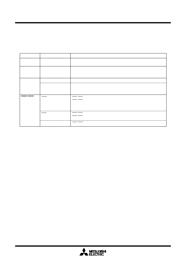
Clock asynchronous serial I/O (UART) mode
Mitsubishi microcomputers
M16C / 62A Group
SINGLE-CHIP 16-BIT CMOS MICROCOMPUTER
127
Table 1.16.7 lists the functions of the input/output pins during UART mode. Note that for a period from
when the UARTi operation mode is selected to when transfer starts, the TxDi pin outputs an "H". (If the N-
channel open-drain is selected, this pin is in floating state.)
Table 1.16.7. Input/output pin functions in UART mode
Pin name
Function
Method of selection
TxDi
(P6
3
, P6
7
, P7
0
)
Serial data output
Serial data input
Programmable I/O port
Transfer clock input
Programmable I/O port
RxDi
(P6
2
, P6
6
, P7
1
)
CLKi
(P6
1
, P6
5
, P7
2
)
Internal/external clock select bit (bit 3 at address 03A0
16
, 03A8
16
, 0378
16
) = "0"
Internal/external clock select bit (bit 3 at address 03A0
16
, 03A8
16
) = "1"
Port P6
1
, P6
5
direction register (bits 1 and 5 at address 03EE
16
) = "0"
(Do not set external clock for UART2)
Port P6
2
, P6
6
and P7
1
direction register (bits 2 and 6 at address 03EE
16
,
bit 1 at address 03EF
16
)= "0"
(Can be used as an input port when performing transmission only)
CTS/RTS disable bit (bit 4 at address 03A4
16
, 03AC
16
, 037C
16
) ="0"
CTS/RTS function select bit (bit 2 at address 03A4
16
, 03AC
16
, 037C
16
) = "0"
Port P6
0
, P6
4
and P7
3
direction register (bits 0 and 4 at address 03EE
16
,
bit 3 at address 03EF
16
) = "0"
CTS/RTS disable bit (bit 4 at address 03A4
16
, 03AC
16
, 037C
16)
= "0"
CTS/RTS function select bit (bit 2 at address 03A4
16
, 03AC
16
, 037C
16
) = "1"
CTS/RTS disable bit (bit 4 at address 03A4
16
, 03AC
16
, 037C
16
) = "1"
CTS input
RTS output
CTSi/RTSi
(P6
0
, P6
4
, P7
3
)

Mitsubishi microcomputers
M16C / 62A Group
SINGLE-CHIP 16-BIT CMOS MICROCOMPUTER
Clock asynchronous serial I/O (UART) mode
128
Transmit enable
bit(TE)
Transmit buffer
empty flag(TI)
Transmit register
empty flag (TXEPT)
Start
bit
Parity
bit
TxDi
CTSi
The above timing applies to the following settings :
∑ Parity is enabled.
∑ One stop bit.
∑ CTS function is selected.
∑ Transmit interrupt cause select bit = "1".
"1"
"0"
"1"
"L"
"H"
"0"
"1"
Tc = 16 (n + 1) / fi or 16 (n + 1) / f
EXT
fi : frequency of BRGi count source (f
1
, f
8
, f
32
)
f
EXT
: frequency of BRGi count source (external clock)
n : value set to BRGi
Transmit interrupt
request bit (IR)
"0"
"1"
Cleared to "0" when interrupt request is accepted, or cleared by software
Transmit enable
bit(TE)
Transmit buffer
empty flag(TI)
TxDi
Transmit register
empty flag (TXEPT)
"0"
"1"
"0"
"1"
"0"
"1"
The above timing applies to the following settings :
∑ Parity is disabled.
∑ Two stop bits.
∑ CTS function is disabled.
∑ Transmit interrupt cause select bit = "0".
Transfer clock
Tc
Tc = 16 (n + 1) / fi or 16 (n + 1) / f
EXT
fi : frequency of BRGi count source (f
1
, f
8
, f
32
)
f
EXT
: frequency of BRGi count source (external clock)
n : value set to BRGi
Transmit interrupt
request bit (IR)
"0"
"1"
Shown in ( ) are bit symbols.
Shown in ( ) are bit symbols.
Tc
Transfer clock
D
0
D
1
D
2
D
3
D
4
D
5
D
6
D
7
ST
P
D
0
D
1
D
2
D
3
D
4
D
5
D
6
D
7
SP
ST
P
SP
D
0
D
1
ST
Stopped pulsing because transmit enable bit = "0"
Stop
bit
Transferred from UARTi transmit buffer register to UARTi transmit register
Start
bit
The transfer clock stops momentarily as CTS is "H" when the stop bit is checked.
The transfer clock starts as the transfer starts immediately CTS changes to "L".
Data is set in UARTi transmit buffer register
D
0
D
1
D
2
D
3
D
4
D
5
D
6
D
7
ST
SP
D
8
D
0
D
1
D
2
D
3
D
4
D
5
D
6
D
7
ST
D
8
D
0
D
1
ST
SPSP
Transferred from UARTi transmit buffer register to UARTi transmit register
Stop
bit
Stop
bit
Data is set in UARTi transmit buffer register.
"0"
SP
Cleared to "0" when interrupt request is accepted, or cleared by software
∑ Example of transmit timing when transfer data is 8 bits long (parity enabled, one stop bit)
∑ Example of transmit timing when transfer data is 9 bits long (parity disabled, two stop bits)
Figure 1.16.17. Typical transmit timings in UART mode(UART0,UART1)

Clock asynchronous serial I/O (UART) mode
Mitsubishi microcomputers
M16C / 62A Group
SINGLE-CHIP 16-BIT CMOS MICROCOMPUTER
129
Figure 1.16.18. Typical transmit timings in UART mode(UART2)
D
0
D
1
D
2
D
3
D
4
D
5
D
6
D
7
ST
P
Start
bit
Parity
bit
Cleared to "0" when interrupt request is accepted, or cleared by software
D
0
D
1
D
2
D
3
D
4
D
5
D
6
D
7
ST
P
Tc
SP
Stop
bit
Data is set in UART2 transmit buffer register
Transferred from UART2 transmit buffer register to UARTi transmit register
SP
Transmit enable
bit(TE)
Transmit buffer
empty flag(TI)
Transmit register
empty flag (TXEPT)
"0"
"1"
"0"
"1"
"0"
"1"
Transmit interrupt
request bit (IR)
"0"
"1"
Transfer clock
TxD
2
The above timing applies to the following settings :
∑ Parity is enabled.
∑ One stop bit.
∑ Transmit interrupt cause select bit = "1".
Tc = 16 (n + 1) / fi
fi : frequency of BRG2 count source (f
1
, f
8
, f
32
)
n : value set to BRG2
Shown in ( ) are bit symbols.
Note
Note: The transmit is started with overflow timing of BRG after having written in a value at the transmit buffer in the above timing.
∑ Example of transmit timing when transfer data is 8 bits long (parity enabled, one stop bit)

Mitsubishi microcomputers
M16C / 62A Group
SINGLE-CHIP 16-BIT CMOS MICROCOMPUTER
Clock asynchronous serial I/O (UART) mode
130
(b) Function for switching serial data logic (UART2)
When the data logic select bit (bit 6 of address 037D
16
) is assigned 1, data is inverted in writing to the
transmission buffer register or reading the reception buffer register. Figure 1.16.20 shows the ex-
ample of timing for switching serial data logic.
Figure 1.16.20. Timing for switching serial data logic
ST : Start bit
P : Even parity
SP : Stop bit
D0
D1
D2
D3
D4
D5
D6
D7
P
SP
ST
SP
ST
D3
D4
D5
D6
D7
P
D0
D1
D2
Transfer clock
TxD
2
(no reverse)
TxD
2
(reverse)
"H"
"L"
"H"
"L"
"H"
"L"
∑ When LSB first, parity enabled, one stop bit
∑ Example of receive timing when transfer data is 8 bits long (parity disabled, one stop bit)
Figure 1.16.19. Typical receive timing in UART mode
(a) Sleep mode (UART0, UART1)
This mode is used to transfer data between specific microcomputers among multiple microcomputers
connected using UARTi. The sleep mode is selected when the sleep select bit (bit 7 at addresses
03A0
16
, 03A8
16
) is set to "1" during reception. In this mode, the unit performs receive operation when
the MSB of the received data = "1" and does not perform receive operation when the MSB = "0".
D
0
Start bit
Sampled "L"
Receive data taken in
BRGi count
source
Receive enable bit
RxDi
Transfer clock
Receive
complete flag
RTSi
Stop bit
"1"
"0"
"0"
"1"
"H"
"L"
The above timing applies to the following settings :
∑Parity is disabled.
∑One stop bit.
∑RTS function is selected.
Receive interrupt
request bit
"0"
"1"
Transferred from UARTi receive register to
UARTi receive buffer register
Reception triggered when transfer clock
is generated by falling edge of start bit
D
7
D
1
Cleared to "0" when interrupt request is accepted, or cleared by software

Clock asynchronous serial I/O (UART) mode
Mitsubishi microcomputers
M16C / 62A Group
SINGLE-CHIP 16-BIT CMOS MICROCOMPUTER
131
(c) TxD, RxD I/O polarity reverse function (UART2)
This function is to reverse T
X
D pin output and R
X
D pin input. The level of any data to be input or output
(including the start bit, stop bit(s), and parity bit) is reversed. Set this function to "0" (not to reverse) for
usual use.
(d) Bus collision detection function (UART2)
This function is to sample the output level of the T
X
D pin and the input level of the R
X
D pin at the rising
edge of the transfer clock; if their values are different, then an interrupt request occurs. Figure 1.16.21
shows the example of detection timing of a bus collision (in UART mode).
Figure 1.16.21. Detection timing of a bus collision (in UART mode)
ST : Start bit
SP : Stop bit
ST
ST
SP
SP
Transfer clock
TxD
2
RxD
2
Bus collision detection
interrupt request signal
"H"
"L"
"H"
"L"
"H"
"L"
"1"
"0"
Bus collision detection
interrupt request bit
"1"
"0"

Mitsubishi microcomputers
M16C / 62A Group
SINGLE-CHIP 16-BIT CMOS MICROCOMPUTER
Clock asynchronous serial I/O (UART) mode
132
Item
Specification
Transfer data format
∑ Transfer data 8-bit UART mode (bit 2 through bit 0 of address 0378
16
= "101
2
")
∑ One stop bit (bit 4 of address 0378
16
= "0")
∑ With the direct format chosen
Set parity to "even" (bit 5 and bit 6 of address 0378
16
= "1" and "1" respectively)
Set data logic to "direct" (bit 6 of address 037D
16
= "0").
Set transfer format to LSB (bit 7 of address 037C
16
= "0").
∑ With the inverse format chosen
Set parity to "odd" (bit 5 and bit 6 of address 0378
16
= "0" and "1" respectively)
Set data logic to "inverse" (bit 6 of address 037D
16
= "1")
Set transfer format to MSB (bit 7 of address 037C
16
= "1")
Transfer clock
∑ With the internal clock chosen (bit 3 of address 0378
16
= "0") : fi / 16 (n + 1) (Note 1) : fi=f
1
, f
8
, f
32
(Do not set external clock)
Transmission / reception control
_______
_______
∑ Disable the CTS and RTS function (bit 4 of address 037C
16
= "1")
Other settings
∑ The sleep mode select function is not available for UART2
∑ Set transmission interrupt factor to "transmission completed" (bit 4 of address 037D
16
= "1")
Transmission start condition ∑ To start transmission, the following requirements must be met:
- Transmit enable bit (bit 0 of address 037D
16
) = "1"
- Transmit buffer empty flag (bit 1 of address 037D
16
) = "0"
Reception start condition
∑ To start reception, the following requirements must be met:
- Reception enable bit (bit 2 of address 037D
16
) = "1"
- Detection of a start bit
∑ When transmitting
When data transmission from the UART2 transmit register is completed
(bit 4 of address 037D
16
= "1")
∑ When receiving
When data transfer from the UART2 receive register to the UART2 receive
buffer register is completed
Error detection
∑ Overrun error (see the specifications of clock-asynchronous serial I/O) (Note 2)
∑ Framing error (see the specifications of clock-asynchronous serial I/O)
∑ Parity error (see the specifications of clock-asynchronous serial I/O)
- On the reception side, an "L" level is output from the T
X
D
2
pin by use of the parity error
signal output function (bit 7 of address 037D
16
= "1") when a parity error is detected
- On the transmission side, a parity error is detected by the level of input to
the R
X
D
2
pin when a transmission interrupt occurs
∑ The error sum flag (see the specifications of clock-asynchronous serial I/O)
(3) Clock-asynchronous serial I/O mode (used for the SIM interface)
The SIM interface is used for connecting the microcomputer with a memory card or the like; adding some
extra settings in UART2 clock-asynchronous serial I/O mode allows the user to effect this function. Table
1.16.8 shows the specifications of clock-asynchronous serial I/O mode (used for the SIM interface).
Interrupt request
generation timing
Note 1: `n' denotes the value 00
16
to FF
16
that is set to the UART2 bit rate generator.
Note 2: If an overrun error occurs, the UART2 receive buffer will have the next data written in. Note also
that the UART2 receive interrupt request bit is not set to "1".
Table 1.16.8. Specifications of clock-asynchronous serial I/O mode (used for the SIM interface)

Clock asynchronous serial I/O (UART) mode
Mitsubishi microcomputers
M16C / 62A Group
SINGLE-CHIP 16-BIT CMOS MICROCOMPUTER
133
Figure 1.16.22. Typical transmit/receive timing in UART mode (used for the SIM interface)
Transmit enable
bit(TE)
Transmit buffer
empty flag(TI)
Transmit register
empty flag (TXEPT)
D
0
D
1
D
2
D
3
D
4
D
5
D
6
D
7
ST
P
Start
bit
Parity
bit
The above timing applies to the following settings :
∑ Parity is enabled.
∑ One stop bit.
∑ Transmit interrupt cause select bit = "1".
"0"
"1"
"0"
"1"
"0"
"1"
Tc = 16 (n + 1) / fi
fi : frequency of BRG2 count source (f
1
, f
8
, f
32
)
n : value set to BRG2
Transmit interrupt
request bit (IR)
"0"
"1"
D
0
D
1
D
2
D
3
D
4
D
5
D
6
D
7
ST
P
Shown in ( ) are bit symbols.
Tc
Transfer clock
SP
Stop
bit
Data is set in UART2 transmit buffer register
SP
An "L" level returns from TxD
2
due to
the occurrence of a parity error.
The level is detected by the
interrupt routine.
The level is
detected by the
interrupt routine.
Receive enable
bit (RE)
Receive complete
flag (RI)
D
0
D
1
D
2
D
3
D
4
D
5
D
6
D
7
ST
P
Start
bit
Parity
bit
RxD
2
The above timing applies to the following settings :
∑ Parity is enabled.
∑ One stop bit.
∑ Transmit interrupt cause select bit = "0".
"0"
"1"
"0"
"1"
Tc = 16 (n + 1) / fi
fi : frequency of BRG2 count source (f
1
, f
8
, f
32
)
n : value set to BRG2
Receive interrupt
request bit (IR)
"0"
"1"
D
0
D
1
D
2
D
3
D
4
D
5
D
6
D
7
ST
P
SP
Shown in ( ) are bit symbols.
Tc
Transfer clock
SP
Stop
bit
An "L" level returns from TxD
2
due to
the occurrence of a parity error.
TxD
2
Read to receive buffer
Read to receive buffer
D
0
D
1
D
2
D
3
D
4
D
5
D
6
D
7
ST
P
Signal conductor level
(Note 2)
D
0
D
1
D
2
D
3
D
4
D
5
D
6
D
7
ST
P
SP
SP
D
0
D
1
D
2
D
3
D
4
D
5
D
6
D
7
ST
P
D
0
D
1
D
2
D
3
D
4
D
5
D
6
D
7
ST
P
SP
SP
TxD
2
RxD
2
Signal conductor level
(Note 2)
Note 2: Equal in waveform because TxD
2
and RxD
2
are connected.
Transferred from UART2 transmit buffer register to UART2 transmit register
Cleared to "0" when interrupt request is accepted, or cleared by software
Cleared to "0" when interrupt request is accepted, or cleared by software
Note 1: The transmit is started with overflow timing of BRG after having written in a value at the transmit buffer in the above timing.
Note 1

Mitsubishi microcomputers
M16C / 62A Group
SINGLE-CHIP 16-BIT CMOS MICROCOMPUTER
Clock asynchronous serial I/O (UART) mode
134
(a) Function for outputting a parity error signal
During reception, with the error signal output enable bit (bit 7 of address 037D
16
) assigned "1", you
can output an "L" level from the T
X
D
2
pin when a parity error is detected. And during transmission,
comparing with the case in which the error signal output enable bit (bit 7 of address 037D
16
) is as-
signed "0", the transmission completion interrupt occurs in the half cycle later of the transfer clock.
Therefore parity error signals can be detected by a transmission completion interrupt program. Figure
1.16.23 shows the output timing of the parity error signal.
Figure 1.16.23. Output timing of the parity error signal
ST : Start bit
P : Even Parity
SP : Stop bit
D0
D1
D2
D3
D4
D5
D6
D7
P
SP
ST
Hi-Z
Transfer
clock
RxD
2
TxD
2
Receive
complete flag
"H"
"L"
"H"
"L"
"H"
"L"
"1"
∑ LSB first
"0"
(b) Direct format/inverse format
Connecting the SIM card allows you to switch between direct format and inverse format. If you choose
the direct format, D
0
data is output from TxD
2
. If you choose the inverse format, D
7
data is inverted
and output from TxD
2
.
Figure 1.16.24 shows the SIM interface format.
Figure 1.16.24. SIM interface format
P : Even parity
D0
D1
D2
D3
D4
D5
D6
D7
P
Transfer
clcck
TxD
2
(direct)
TxD
2
(inverse)
D7
D6
D5
D4
D3
D2
D1
D0
P

Clock asynchronous serial I/O (UART) mode
Mitsubishi microcomputers
M16C / 62A Group
SINGLE-CHIP 16-BIT CMOS MICROCOMPUTER
135
Figure 1.16.25 shows the example of connecting the SIM interface. Connect T
X
D
2
and R
X
D
2
and apply
pull-up.
Figure 1.16.25. Connecting the SIM interface
Microcomputer
SIM card
TxD
2
RxD
2
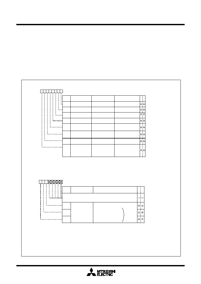
Mitsubishi microcomputers
M16C / 62A Group
SINGLE-CHIP 16-BIT CMOS MICROCOMPUTER
UART2 Special Mode Register
136
UART2 Special Mode Register
The UART2 special mode register (address 0377
16
) is used to control UART2 in various ways.
Figure 1.16.26 shows the UART2 special mode register.
Bit 0 of the UART2 special mode register (0377
16
) is used as the I
2
C mode select bit.
Setting "1" in the I
2
C mode select bit (bit 0) goes the circuit to achieve the I
2
C bus (simplified I
2
C bus)
interface effective.
Table 1.16.9 shows the relation between the I
2
C mode select bit and respective control workings.
Since this function uses clock-synchronous serial I/O mode, set this bit to "0" in UART mode.
Figure 1.16.26. UART2 special mode register
UART2 special mode register
Symbol
Address
When reset
U2SMR
0377
16
00
16
b7
b6
b5
b4 b3
b2
b1
b0
Bit
name
Bit
symbol
W
R
Function
(During UART mode)
Function
(During clock synchronous
serial I/O mode)
ABSCS
ACSE
SSS
I
2
C mode select bit
Bus busy flag
0 : STOP condition detected
1 : START condition detected
SCL L sync output
enable bit
Bus collision detect
sampling clock select bit
Arbitration lost detecting
flag control bit
0 : Normal mode
1 : I
2
C mode
0 : Update per bit
1 : Update per byte
IICM
ABC
BBS
LSYN
0 : Ordinary
1 : Falling edge of RxD
2
0 : Disabled
1 : Enabled
Transmit start condition
select bit
Must always be "0"
0 : Rising edge of transfer
clock
1 : Underflow signal of timer A0
Auto clear function
select bit of transmit
enable bit
0 : No auto clear function
1 : Auto clear at occurrence of
bus collision
Must always be "0"
Must always be "0"
Must always be "0"
Must always be "0"
Must always be "0"
Must always be "0"
Note 1: Nothing but "0" may be written.
Note 2: When not in I
2
C mode, do not set this bit by writing a "1". During normal mode, fix it to "0". When this
bit = "0", UART2 special mode register 3 (U2SMR3 at address 0375
16
) bits 7 to 5 (DL2 to DL0 = SDA
digital delay setup bits) are initialized to "000", with the analog delay circuit selected. Also, when SDDS
= "0", the U2SMR3 register cannot be read or written to.
Note 3: When analog delay is selected, only the analog delay value is effective; when digital delay is selected,
only the digital delay value is effective.
(Note1)
SDDS
SDA digital delay select
bit (Note 2, Note 3)
Must always be "0"
0 : Analog delay output
is selected
1 : Digital delay output
is selected
(must always be "0" when
not using I C mode)
2
UART2 special mode register 3 (I C bus exclusive use register)
Symbol
Address
When reset
U2SMR3
0375
16
Indeterminate
(However, when SDDS = "1", the initial value is "00
16
")
b7
b6 b5
b4
b3
b2
b1
b0
Bit name
Bit
symbol
W
R
Function
(I C bus exclusive use register)
DL2
SDA digital delay setup
bit
(Note 1, Note 2, Note 3,
Note 4)
DL0
DL1
0 0 0 : Analog delay is selected
0 0 1 : 1 to 2 cycle(s) of 1/f(X
IN
)
0 1 0 : 2 to 3 cycles of 1/f(X
IN
)
0 1 1 : 3 to 4 cycles of 1/f(X
IN
)
1 0 0 : 4 to 5 cycles of 1/f(X
IN
)
1 0 1 : 5 to 6 cycles of 1/f(X
IN
)
1 1 0 : 6 to 7 cycles of 1/f(X
IN
)
1 1 1 : 7 to 8 cycles of 1/f(X
IN
)
2
Nothing is assigned.
In an attempt to write to these bits, write "0". The value, if read, turns out to be
indeterminate. However, when SDDS = "1", the value "0" is read out (Note 1)
2
b7 b6 b5
Note 1: This bit can be read or written to when UART2 special mode register (U2SMR at address 0377
16
) bit
7 (SDDS: SDA digital delay select bit) = "1". When the initial value of UART2 special mode register 3
(U2SMR3) is read after setting SDDS = "1", the value is "00
16
". When writing to UART2 special mode
register 3 (U2SMR3) after setting SDDS = "1", be sure to write 0's to bits 0≠4. When SDDS = "0",
this register cannot be written to; when read, the value is indeterminate.
Note 2: These bits are initialized to "000" when SDDS = "0", with the analog delay circuit selected. After a reset,
these bits are set to "000", with the analog delay circuit selected. However, because these bits can be
read only when SDDS = "1", the value read from these bits when SDDS = "0" is indeterminate.
Note 3: When analog delay is selected, only the analog delay value is effective; when digital delay is selected,
only the digital delay value is effective.
Note 4: The amount of delay varies with the load on SCL and SDA pins. Also, when using an external clock, the
amount of delay increases by about 100 ns, so be sure to take this into account when using the device.
Digital delay
is selected

Mitsubishi microcomputers
M16C / 62A Group
SINGLE-CHIP 16-BIT CMOS MICROCOMPUTER
UART2 Special Mode Register
137
Function
Normal mode
I
2
C mode (Note 1)
Factor of interrupt number 15 (Note 2)
UART2 transmission
No acknowledgment detection (NACK)
Factor of interrupt number 16 (Note 2)
UART2 reception
Start condition detection or stop
condition detection
UART2 transmission output delay
Not delayed
Delayed
P7
0
at the time when UART2 is in use
TxD
2
(output)
SDA (input/output) (Note 3)
P7
1
at the time when UART2 is in use
RxD
2
(input)
SCL (input/output)
P7
2
at the time when UART2 is in use
CLK
2
P7
2
DMA1 factor at the time when 1 1 0 1 is assigned
to the DMA request factor selection bits
UART2 reception
Acknowledgment detection (ACK)
Noise filter width
15ns
50ns
Reading P7
1
Reading the terminal when 0 is
assigned to the direction register
Reading the terminal regardless of the
value of the direction register
1
2
3
4
5
6
7
8
9
Note 1: Make the settings given below when I
2
C mode is in use.
Set 0 1 0 in bits 2, 1, 0 of the UART2 transmission/reception mode register.
Disable the RTS/CTS function. Choose the MSB First function.
Note 2: Follow the steps given below to switch from a factor to another.
1. Disable the interrupt of the corresponding number.
2. Switch from a factor to another.
3. Reset the interrupt request flag of the corresponding number.
4. Set an interrupt level of the corresponding number.
Note 3: Set an initial value of SDA transmission output when serial I/O is invalid.
Factor of interrupt number 10 (Note 2)
Bus collision detection
Acknowledgment detection (ACK)
10
Initial value of UART2 output
H level (when 0 is assigned to
the CLK polarity select bit)
The value set in latch P7
0
when the port is
selected
11
Table 1.16.9. Features in I
2
C mode
P7
0
/TxD
2
/SDA
P7
1
/RxD
2
/SCL
CLK
control
P7
2
/CLK
2
Falling edge
detection
UART2 reception/ACK interrupt
request, DMA1 request
To DMA0, DMA1
To DMA0
2
P7
0
through P7
2
conforming to the simplified I C bus
I/O
Timer
UART2
Timer
UART2
IICM=1 (SDDS=0) or
DL=000 (SDDS=1)
IICM=0
or IICM2=1
IICM=1
and IICM2=0
SDHI
Noize
Filter
Timer
UART2
UART2
I/O
D
T
Q
D
T
Q
D
T
Q
NACK
ACK
UART2
UART2
IICM=1
IICM=0
IICM=0
IICM=1
IICM=1
IICM=0
S
R
Q
IICM=1
IICM=0
I/O
R
Q
ALS
IICM=0 or
DL
000 (SDDS=1)
SDDS=0
or DL=000
SDDS=1 and
DL
000
SWC2
Falling edge of 9 bit
SWC
IICM=1
and IICM2=0
IICM=0
or IICM2=1
Selector
Selector
Selector
Noize
Filter
Noize
Filter
*
With IICM set to 1, the port terminal is to be readable
even if 1 is assigned to P7
1
of the direction register.
Port reading
External clock
Internal clock
9th pulse
Bus collision
detection
Bus collision/start, stop condition
detection interrupt request
UART2 transmission/
NACK interrupt request
Start condition
detection
Stop condition
detection
L-synchronous
output enabling
bit
(Port P7
1
output data latch)
Data bus
Reception register
Bus busy
Transmission
register
Arbitration
Analog
delay
Digital delay
(Divider)
Figure 1.16.27. Functional block diagram for I
2
C mode

Mitsubishi microcomputers
M16C / 62A Group
SINGLE-CHIP 16-BIT CMOS MICROCOMPUTER
UART2 Special Mode Register
138
An attempt to read Port P7
1
(SCL) results in getting the terminal's level regardless of the content of the
port direction register. The initial value of SDA transmission output in this mode goes to the value set in
port P7
0
. The interrupt factors of the bus collision detection interrupt, UART2 transmission interrupt, and
of UART2 reception interrupt turn to the start/stop condition detection interrupt, acknowledgment non-
detection interrupt, and acknowledgment detection interrupt respectively.
The start condition detection interrupt refers to the interrupt that occurs when the falling edge of the SDA
terminal (P7
0
) is detected with the SCL terminal (P7
1
) staying "H". The stop condition detection interrupt
refers to the interrupt that occurs when the rising edge of the SDA terminal (P7
0
) is detected with the SCL
terminal (P7
1
) staying "H". The bus busy flag (bit 2 of the UART2 special mode register) is set to "1" by the
start condition detection, and set to "0" by the stop condition detection.
The acknowledgment non-detection interrupt refers to the interrupt that occurs when the SDA terminal
level is detected still staying "H" at the rising edge of the 9th transmission clock. The acknowledgment
detection interrupt refers to the interrupt that occurs when SDA terminal's level is detected already went
to "L" at the 9th transmission clock. Also, assigning 1 1 0 1 (UART2 reception) to the DMA1 request factor
select bits provides the means to start up the DMA transfer by the effect of acknowledgment detection.
Bit 1 of the UART2 special mode register (0377
16
) is used as the arbitration lost detecting flag control bit.
Arbitration means the act of detecting the nonconformity between transmission data and SDA terminal
data at the timing of the SCL rising edge. This detecting flag is located at bit 11 of the UART2 reception
buffer register (037F
16
, 037E
16
), and "1" is set in this flag when nonconformity is detected. Use the
arbitration lost detecting flag control bit to choose which way to use to update the flag, bit by bit or byte by
byte. When setting this bit to "1" and updated the flag byte by byte if nonconformity is detected, the
arbitration lost detecting flag is set to "1" at the falling edge of the 9th transmission clock.
If update the flag byte by byte, must judge and clear ("0") the arbitration lost detecting flag after complet-
ing the first byte acknowledge detect and before starting the next one byte transmission.
Bit 3 of the UART2 special mode register is used as SCL- and L-synchronous output enable bit. Setting
this bit to "1" goes the P7
1
data register to "0" in synchronization with the SCL terminal level going to "L".
Figure 1.16.27 shows the functional block diagram for I
2
C mode. Setting "1" in the I
2
C mode select bit
(IICM) causes ports P7
0
, P7
1
, and P7
2
to work as data transmission-reception terminal SDA, clock input-
output terminal SCL, and port P7
2
respectively. A delay circuit is added to the SDA transmission output,
so the SDA output changes after SCL fully goes to "L". The SDA digital delay select bit (bit 7 at address
0377
16
) can be used to select between analog delay and digital delay. When digital delay is selected, the
amount of delay can be selected in the range of 2 cycles to 8 cycles of f1 using UART2 special mode
register 3 (at address 0375
16
). Delay circuit select conditions are shown in Table 1.16.10.
Table 1.16.10. Delay circuit select conditions
Digital delay is
selected
001
111
000
(000)
1
0
1
1
1
Analog delay is
selected
No delay
0
0
(000)
IICM
SDDS
DL
Register value
Contents
When digital delay is selected, no analog delay is added. Only
digital delay is effective.
When DL is set to "000", analog delay is selected no matter what
value is set in SDDS.
When SDDS is set to "0", DL is initialized, so that DL ="000".
When IICM = "0", no delay circuit is selected. When IICM = "0",
however, always make sure SDDS = "0".
to

Mitsubishi microcomputers
M16C / 62A Group
SINGLE-CHIP 16-BIT CMOS MICROCOMPUTER
UART2 Special Mode Register
139
1. Bus collision detect sampling clock select bit (Bit 4 of the UART2 special mode register)
0: Rising edges of the transfer clock
CLK
Timer A0
1: Timer A0 overflow
2. Auto clear function select bit of transmt enable bit (Bit 5 of the UART2 special mode register)
CLK
TxD/RxD
Bus collision
detect interrupt
request bit
Transmit
enable bit
3. Transmit start condition select bit (Bit 6 of the UART2 special mode register)
CLK
TxD
Enabling transmission
CLK
TxD
RxD
With "1: falling edge of RxD
2
" selected
0: In normal state
TxD/RxD
Figure 1.16.28. Some other functions added
Some other functions added are explained here. Figure 1.16.28 shows their workings.
Bit 4 of the UART2 special mode register is used as the bus collision detect sampling clock select bit. The
bus collision detect interrupt occurs when the R
X
D
2
level and T
X
D
2
level do not match, but the nonconfor-
mity is detected in synchronization with the rising edge of the transfer clock signal if the bit is set to "0". If
this bit is set to "1", the nonconformity is detected at the timing of the overflow of timer A0 rather than at
the rising edge of the transfer clock.
Bit 5 of the UART2 special mode register is used as the auto clear function select bit of transmit enable
bit. Setting this bit to "1" automatically resets the transmit enable bit to "0" when "1" is set in the bus
collision detect interrupt request bit (nonconformity).
Bit 6 of the UART2 special mode register is used as the transmit start condition select bit. Setting this bit
to "1" starts the TxD transmission in synchronization with the falling edge of the RxD terminal.

Mitsubishi microcomputers
M16C / 62A Group
SINGLE-CHIP 16-BIT CMOS MICROCOMPUTER
UART2 Special Mode Register 2
140
UART2 Special Mode Register 2
UART2 special mode register 2 (address 0376
16
) is used to further control UART2 in I
2
C mode. Figure
1.16.29 shows the UART2 special mode register 2.
UART2 special mode register 2 (I C bus exclusive use register)
Symbol
Address
When reset
U2SMR2
0376
16
00
16
b7
b6 b5
b4
b3
b2
b1
b0
Bit name
Bit
symbol
W
R
Function
STAC
SWC2
SDHI
I C mode select bit 2
SCL wait output bit
0 : Disabled
1 : Enabled
SDA output stop bit
UART2 initialization bit
Clock-synchronous bit
Refer to Table 1.16.11
0 : Disabled
1 : Enabled
IICM2
CSC
SWC
ALS 0
:
Disabled
1 : Enabled
SDA output disable bit
SCL wait output bit 2
0: Enabled
1: Disabled (high impedance)
0 : Disabled
1 : Enabled
0: UART2 clock
1: 0 output
2
SHTC
Start/stop condition
control bit
Set this bit to "1" in I
2
C mode
(refer to Table 1.16.12)
2
Figure 1.16.29. UART2 special mode register 2

Mitsubishi microcomputers
M16C / 62A Group
SINGLE-CHIP 16-BIT CMOS MICROCOMPUTER
UART2 Special Mode Register 2
141
Bit 0 of the UART2 special mode register 2 (address 0376
16
) is used as the I
2
C mode select bit 2. Table
1.16.11 shows the types of control to be changed by I
2
C mode select bit 2 when the I
2
C mode select bit
is set to "1". Table 1.16.12 shows the timing characteristics of detecting the start condition and the stop
condition. Set the start/stop condition control bit (bit 7 of UART2 special mode register 2) to "1" in I
2
C
mode.
Function
IICM2 = 1
IICM2 = 0
Factor of interrupt number 15
No acknowledgment detection (NACK)
UART2 transmission (the rising edge
of the final bit of the clock)
Factor of interrupt number 16
Acknowledgment detection (ACK)
UART2 reception (the falling edge
of the final bit of the clock)
DMA1 factor at the time when 1 1 0 1
is assigned to the DMA request
factor selection bits
Acknowledgment detection (ACK)
UART2 reception (the falling edge of
the final bit of the clock)
Timing for transferring data from the
UART2 reception shift register to the
reception buffer.
The rising edge of the final bit of the
reception clock
The falling edge of the final bit of the
reception clock
Timing for generating a UART2
reception/ACK interrupt request
The rising edge of the final bit of the
reception clock
The falling edge of the final bit of the
reception clock
1
2
3
4
5
3 to 6 cycles < duration for setting-up (Note2)
3 to 6 cycles < duration for holding (Note2)
Note 1 : When the start/stop condition control bit SHTC is "1" .
Note 2 : "Cycles" is in terms of the input oscillation frequency f(X
IN
) of the main clock.
Duration for
setting up
Duration for
holding
SCL
SDA
(Start condition)
SDA
(Stop condition)
Table 1.16.11. Functions changed by I
2
C mode select bit 2
Table 1.16.12. Timing characteristics of detecting the start condition and the stop condition (Note1)

Mitsubishi microcomputers
M16C / 62A Group
SINGLE-CHIP 16-BIT CMOS MICROCOMPUTER
UART2 Special Mode Register 2
142
P7
0
/TxD
2
/SDA
P7
1
/RxD
2
/SCL
CLK
control
P7
2
/CLK
2
Falling edge
detection
UART2 reception/ACK interrupt
request, DMA1 request
To DMA0, DMA1
To DMA0
2
P7
0
through P7
2
conforming to the simplified I C bus
I/O
Timer
UART2
Timer
UART2
IICM=1 (SDDS=0) or
DL=000 (SDDS=1)
IICM=0
or IICM2=1
IICM=1
and IICM2=0
SDHI
Noize
Filter
Timer
UART2
UART2
I/O
D
T
Q
D
T
Q
D
T
Q
NACK
ACK
UART2
UART2
IICM=1
IICM=0
IICM=0
IICM=1
IICM=1
IICM=0
S
R
Q
IICM=1
IICM=0
I/O
R
Q
ALS
IICM=0 or
DL
000 (SDDS=1)
SDDS=0
or DL=000
SDDS=1 and
DL
000
SWC2
Falling edge of 9 bit
SWC
IICM=1
and IICM2=0
IICM=0
or IICM2=1
Selector
Selector
Selector
Noize
Filter
Noize
Filter
*
With IICM set to 1, the port terminal is to be readable
even if 1 is assigned to P7
1
of the direction register.
Port reading
External clock
Internal clock
9th pulse
Bus collision
detection
Bus collision/start, stop condition
detection interrupt request
UART2 transmission/
NACK interrupt request
Start condition
detection
Stop condition
detection
L-synchronous
output enabling
bit
(Port P7
1
output data latch)
Data bus
Reception register
Bus busy
Transmission
register
Arbitration
Analog
delay
Digital delay
(Divider)
Functions available in I
2
C mode are shown in Figure 1.16.30 -- a functional block diagram.
Bit 3 of the UART2 special mode register 2 (address 0376
16
) is used as the SDA output stop bit. Setting
this bit to "1" causes an arbitration loss to occur, and the SDA pin turns to high-impedance state at the
instant when the arbitration lost detecting flag is set to "1".
Bit 1 of the UART2 special mode register 2 (address 0376
16
) is used as the clock synchronization bit.
With this bit set to "1" at the time when the internal SCL is set to "H", the internal SCL turns to "L" if the
falling edge is found in the SCL pin; and the baud rate generator reloads the set value, and start counting
within the "L" interval. When the internal SCL changes from "L" to "H" with the SCL pin set to "L", stops
counting the baud rate generator, and starts counting it again when the SCL pin turns to "H". Due to this
function, the UART2 transmission-reception clock becomes the logical product of the signal flowing
through the internal SCL and that flowing through the SCL pin. This function operates over the period
from the moment earlier by a half cycle than falling edge of the UART2 first clock to the rising edge of the
ninth bit. To use this function, choose the internal clock for the transfer clock.
Bit 2 of the UART2 special mode register 2 (0376
16
) is used as the SCL wait output bit. Setting this bit to
"1" causes the SCL pin to be fixed to "L" at the falling edge of the ninth bit of the clock. Setting this bit to
"0" frees the output fixed to "L".
Figure 1.16.30. Functional block diagram for I
2
C mode

Mitsubishi microcomputers
M16C / 62A Group
SINGLE-CHIP 16-BIT CMOS MICROCOMPUTER
UART2 Special Mode Register 2
143
Bit 4 of the UART2 special mode register 2 (address 0376
16
) is used as the UART2 initialization bit.
Setting this bit to "1", and when the start condition is detected, the microcomputer operates as follows.
(1) The transmission shift register is initialized, and the content of the transmission register is transferred
to the transmission shift register. This starts transmission by dealing with the clock entered next as the
first bit. The UART2 output value, however, doesn't change until the first bit data is output after the
entrance of the clock, and remains unchanged from the value at the moment when the microcomputer
detected the start condition.
(2) The reception shift register is initialized, and the microcomputer starts reception by dealing with the
clock entered next as the first bit.
(3) The SCL wait output bit turns to "1". This turns the SCL pin to "L" at the falling edge of the ninth bit of
the clock.
Starting to transmit/receive signals to/from UART2 using this function doesn't change the value of the
transmission buffer empty flag. To use this function, choose the external clock for the transfer clock.
Bit 5 of the UART2 special mode register 2 (0376
16
) is used as the SCL pin wait output bit 2. Setting this
bit to "1" with the serial I/O specified allows the user to forcibly output an "1" from the SCL pin even if
UART2 is in operation. Setting this bit to "0" frees the "L" output from the SCL pin, and the UART2 clock
is input/output.
Bit 6 of the UART2 special mode register 2 (0376
16
) is used as the SDA output disable bit. Setting this bit
to "1" forces the SDA pin to turn to the high-impedance state. Refrain from changing the value of this bit
at the rising edge of the UART2 transfer clock. There can be instances in which arbitration lost detecting
flag is turned on.

Mitsubishi microcomputers
M16C / 62A Group
SINGLE-CHIP 16-BIT CMOS MICROCOMPUTER
S I/O3, 4
144
S I/O3, 4
S I/O3 and S I/O4 are exclusive clock-synchronous serial I/Os.
Figure 1.16.31 shows the S I/O3, 4 block diagram, and Figure 1.16.32 shows the S I/O3, 4 related register.
Table 1.16.13 shows the specifications of S I/O3, 4.
Figure 1.16.31. S I/O3, 4 block diagram
S I/Oi transmission/reception register (8)
S I/O counter i (3)
Synchronous
circuit
f
1
f
8
f
32
Data bus
8
S I/Oi
interrupt request
SMi5 LSB MSB
SMi2
SMi3
SMi3
SMi6
SMi1
SMi0
P9
0/
CLK
3
(P9
5/
CLK
4
)
P9
2/
S
OUT3
(P9
6/
S
OUT4
)
P9
1/
S
IN3
(P9
7/
S
IN4
)
Bit rate generator (8)
SMi6
Note: i = 3, 4.
ni = A value set in the S I/O i bit rate generator (0363
16
, 0367
16
).
1/(ni+1)
1/2
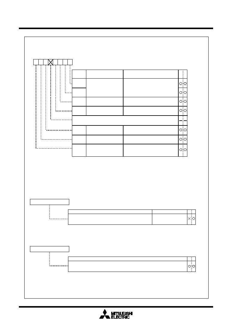
Mitsubishi microcomputers
M16C / 62A Group
SINGLE-CHIP 16-BIT CMOS MICROCOMPUTER
S I/O3, 4
145
SI/Oi bit rate generator (Note 1, 2)
b7
b0
Symbol
Address
When reset
S3BRG
0363
16
Indeterminate
S4BRG
0367
16
Indeterminate
Indeterminate
Assuming that set value = n, BRGi divides the count
source by n + 1
00
16
to FF
16
Values that can be set
W
R
SI/Oi transmit/receive register (Note)
b7
b0
Symbol
Address
When reset
S3TRR
0360
16
Indeterminate
S4TRR
0364
16
Indeterminate
Indeterminate
Transmission/reception starts by writing data to this register.
After transmission/reception finishes, reception data is input.
W
R
S I/Oi control register (i = 3, 4) (Note 1)
Symbol
Address
When reset
SiC
0362
16
, 0366
16
40
16
b7
b6
b5
b4 b3
b2
b1
b0
W
R
Description
SMi5
SMi1
SMi0
SMi3
SMi6
SMi7
Internal synchronous
clock select bit
Transfer direction select
bit
S I/Oi port select bit
(Note 2)
S
OUT
i initial value
set bit
0 0 : Selecting f
1
0 1 : Selecting f
8
1 0 : Selecting f
32
1 1 : Must not be set.
b1 b0
0 : External clock
1 : Internal clock
Effective when SMi3 = 0
0 : L output
1 : H output
0 : Input-output port
1 : S
OUT
i output, CLK function
Bit name
Bit
symbol
Synchronous clock
select bit (Note 2)
0 : LSB first
1 : MSB first
SMi2
S
OUT
i output disable bit
0 : S
OUT
i output
1 : S
OUT
i output disable
(high impedance)
Note 1: Set "1" in bit 2 of the protection register (000A
16
) in advance to write to the
S I/Oi control register (i = 3, 4).
Note 2:
When using the port as an input/output port by setting the SI/Oi port
select bit (i = 3, 4) to
"0"
, be sure to set the sync clock select bit to
"1"
.
Nothing is assigned.
In an attempt to write to this bit, write "0". The value, if read, turns out to be "0".
Note 1: Write a value to this register while transmit/receive halts.
Note 2: Use MOV instruction to write to this register.
Note: Write a value to this register while transmit/receive halts.
Figure 1.16.32. S I/O3, 4 related register

Mitsubishi microcomputers
M16C / 62A Group
SINGLE-CHIP 16-BIT CMOS MICROCOMPUTER
S I/O3, 4
146
Table 1.16.13. Specifications of S I/O3, 4
Note 1: n is a value from 00
16
through FF
16
set in the S I/Oi bit rate generator (i = 3, 4).
Note 2: With the external clock selected:
∑ Before data can be written to the SI/Oi transmit/receive register (addresses 0360
16
, 0364
16
), the
CLKi pin input must be in the high state. Also, before rewriting the SI/Oi Control Register (addresses
0362
16
, 0366
16
)'s bit 7 (S
OUT
i initial value set bit), make sure the CLKi pin input is held high.
∑ The S I/Oi circuit keeps on with the shift operation as long as the synchronous clock is entered in it,
so stop the synchronous clock at the instant when it counts to eight. The internal clock, if selected,
automatically stops.
Note 3: If the internal clock is used for the synchronous clock, the transfer clock signal stops at the "H" state.
Item
Transfer data format
Transfer clock
Conditions for
transmission/
reception start
Interrupt request
generation timing
Select function
Precaution
Specifications
∑ Transfer data length: 8 bits
∑ With the internal clock selected (bit 6 of 0362
16
, 0366
16
= "1"): f
1
/2(ni+1),
f
8
/2(ni+1), f
32
/2(ni+1) (Note 1)
∑ With the external clock selected (bit 6 of 0362
16
, 0366
16
= 0):Input from the CLKi terminal (Note 2)
∑ To start transmit/reception, the following requirements must be met:
- Select the synchronous clock (use bit 6 of 0362
16
, 0366
16
).
Select a frequency dividing ratio if the internal clock has been selected (use bits
0 and 1 of 0362
16
, 0366
16
).
- S
OUT
i initial value set bit (use bit 7 of 0362
16
, 0366
16
)= 1.
- S I/Oi port select bit (bit 3 of 0362
16
, 0366
16
) = 1.
- Select the transfer direction (use bit 5 of 0362
16
, 0366
16
)
-Write transfer data to SI/Oi transmit/receive register (0360
16
, 0364
16
)
∑ To use S I/Oi interrupts, the following requirements must be met:
- Clear the SI/Oi interrupt request bit before writing transfer data to the SI/Oi
transmit/receive register (bit 3 of 0049
16
, 0048
16
) = 0.
∑ Rising edge of the last transfer clock. (Note 3)
∑ LSB first or MSB first selection
Whether transmission/reception begins with bit 0 (LSB) or bit 7 (MSB) can be
selected.
∑ Function for setting an S
OUT
i initial value selection
When using an external clock for the transfer clock, the user can choose the
S
OUT
i pin output level during a non-transfer time. For details on how to set, see
Figure 1.16.33.
∑ Unlike UART0≠2, SI/Oi (i = 3, 4) is not divided for transfer register and buffer.
Therefore, do not write the next transfer data to the SI/Oi transmit/receive register
(addresses 0360
16
, 0364
16
) during a transfer.
∑ When the internal clock is selected for the transfer clock, S
OUT
i holds the last data
for a 1/2 transfer clock period after it finished transferring and then goes to a high-
impedance state. However, if the transfer data is written to the SI/Oi transmit/
receive register (addresses 0360
16
, 0364
16
) during this time, S
OUT
i is placed in
the high-impedance state immediately upon writing and the data hold time is
thereby reduced.

Mitsubishi microcomputers
M16C / 62A Group
SINGLE-CHIP 16-BIT CMOS MICROCOMPUTER
S I/O3, 4
147
Functions for setting an S
OUT
i initial value
When using an external clock for the transfer clock, the S
OUTi
pin output level during a non-transfer
time can be set to the high or the low state. Figure 1.16.33 shows the timing chart for setting an S
OUTi
initial value and how to set it.
Figure 1.16.33. Timing chart for setting S
OUT
i's initial value and how to set it
S I/Oi operation timing
Figure 1.16.34 shows the S I/Oi operation timing
D
7
D
0
D
1
D
2
D
3
D
4
D
5
D
6
(i= 3, 4)
(i= 3, 4)
Hiz
Hiz
(i= 3, 4)
1.5 cycle (max)
SI/Oi internal clock
Transfer clock
(Note 1)
Signal written to the S I/Oi
transmit/receive register
S I/Oi output S
OUT
i
S I/Oi input S
IN
i
SI/Oi interrupt request
bit
Note2
Note 1: With the internal clock selected for the transfer clock, the frequency dividing ratio can be selected using bits 0 and 1 of the S I/Oi control
register. (i=3,4) (No frequency division, 8-division frequency, 32-division frequency.)
Note 2: With the internal clock selected for the transfer clock, the S
OUT
i (i = 3, 4) pin becomes to the high-impedance state after the transfer finishes.
Note 3: Shown above is the case where the S
OUT
i (i = 3, 4) port select bit ="1".
"H"
"L"
"H"
"L"
"H"
"L"
"H"
"L"
"H"
"L"
"1"
"0"
Figure 1.16.34. S I/Oi operation timing chart
S I/Oi port select bit SMi3 = 0
SOUTi initial value select bit
SMi7 = 1
(S
OUT
i: Internal "H" level)
S I/Oi port select bit
SMi3 = 0 1
(Port select: Normal port S
OUT
i)
S
OUT
i terminal = "H" output
Signal written to the S I/Oi register
="L" "H" "L"
(Falling edge)
S
OUT
i terminal = Outputting
stored data in the S I/Oi transmission/
reception register
Signal written to the S I/Oi
transmit/receive register
S
OUT
i (internal)
S
OUT
i's initial value
set bit (SMi7)
S
OUT
i terminal output
S I/Oi port select bit
(SMi3)
Setting the S
OUT
i
initial value to H
Port selection
(normal port S
OUT
i)
D0
(i = 3, 4)
Initial value = "H" (Note)
Port output
D0
(Example) With "H" selected for S
OUT
i:
Note: The set value is output only when the external clock has been selected. When
initializing S
OUT
i, make sure the CLKi pin input is held "H" level.
If the internal clock has been selected or if S
OUT
output disable has been set,
this output goes to the high-impedance state.

Mitsubishi microcomputers
M16C / 62A Group
SINGLE-CHIP 16-BIT CMOS MICROCOMPUTER
A-D Converter
148
Item
Performance
Method of A-D conversion Successive approximation (capacitive coupling amplifier)
Analog input voltage (Note 1) 0V to AV
CC
(V
CC
)
Operating clock
AD
(Note 2) V
CC
= 5V
f
AD
/divide-by-2 of f
AD
/divide-by-4 of f
AD
, f
AD
=f(X
IN
)
V
CC
= 3V
divide-by-2 of f
AD
/divide-by-4 of f
AD
, f
AD
=f(X
IN
)
Resolution
8-bit or 10-bit (selectable)
Absolute precision
V
CC
= 5V
∑ Without sample and hold function
±
3LSB
∑ With sample and hold function (8-bit resolution)
±
2LSB
∑ With sample and hold function (10-bit resolution)
AN
0
to AN
7
input :
±
3LSB
ANEX0 and ANEX1 input (including mode in which external
operation amp is connected) :
±
7LSB
V
CC
= 3V
∑ Without sample and hold function (8-bit resolution)
±
2LSB
Operating modes
One-shot mode, repeat mode, single sweep mode, repeat sweep mode 0,
and repeat sweep mode 1
Analog input pins
8pins (AN
0
to AN
7
) + 2pins (ANEX0 and ANEX1)
A-D conversion start condition ∑ Software trigger
A-D conversion starts when the A-D conversion start flag changes to "1"
∑ External trigger (can be retriggered)
A-D conversion starts when the A-D conversion start flag is "1" and the
___________
AD
TRG
/P9
7
input changes from "H" to "L"
Conversion speed per pin ∑ Without sample and hold function
8-bit resolution: 49
AD
cycles, 10-bit resolution: 59
AD
cycles
∑ With sample and hold function
8-bit resolution: 28
AD
cycles, 10-bit resolution: 33
AD
cycles
A-D Converter
The A-D converter consists of one 10-bit successive approximation A-D converter circuit with a capacitive coupling
amplifier. Pins P10
0
to P10
7
, P9
5
, and P9
6
also function as the analog signal input pins. The direction registers of
these pins for A-D conversion must therefore be set to input. The Vref connect bit (bit 5 at address 03D7
16
) can be
used to isolate the resistance ladder of the A-D converter from the reference voltage input pin (V
REF
) when the A-D
converter is not used. Doing so stops any current flowing into the resistance ladder from V
REF
, reducing the power
dissipation. When using the A-D converter, start A-D conversion only after setting bit 5 of 03D7
16
to connect V
REF
.
The result of A-D conversion is stored in the A-D registers of the selected pins. When set to 10-bit precision, the low
8 bits are stored in the even addresses and the high 2 bits in the odd addresses. When set to 8-bit precision, the low
8 bits are stored in the even addresses.
Table 1.17.1 shows the performance of the A-D converter. Figure 1.17.1 shows the block diagram of the
A-D converter, and Figures 1.17.2 and 1.17.3 show the A-D converter-related registers.
Note 1: Does not depend on use of sample and hold function.
Note 2: Divide the frequency if f(X
IN
) exceeds 10MH
Z
, and make
AD
frequency equal to or less than 10MHz.
Without sample and hold function, set the
AD
frequency to 250kH
Z
min.
With the sample and hold function, set the
AD
frequency to 1MH
Z
min.
Table 1.17.1. Performance of A-D converter

Mitsubishi microcomputers
M16C / 62A Group
SINGLE-CHIP 16-BIT CMOS MICROCOMPUTER
A-D Converter
149
Figure 1.17.1. Block diagram of A-D converter
1/2
AD
1/2
f
AD
A-D conversion rate
selection
(03C1
16
, 03C0
16
)
(03C3
16
, 03C2
16
)
(03C5
16
, 03C4
16
)
(03C7
16
, 03C6
16
)
(03C9
16
, 03C8
16
)
(03CB
16
, 03CA
16
)
(03CD
16
, 03CC
16
)
(03CF
16
, 03CE
16
)
CKS1=1
CKS0=0
0 0 : Normal operation
0 1 : ANEX0
1 0 : ANEX1
1 1 : External op-amp mode
A-D register 0(16)
A-D register 1(16)
A-D register 2(16)
A-D register 3(16)
A-D register 4(16)
A-D register 5(16)
A-D register 6(16)
A-D register 7(16)
Resistor ladder
ANEX1
ANEX0
Successive conversion register
OPA1,OPA0=0,1
OPA0=1
OPA1=1
OPA1,OPA0=1,1
AN
0
AN
1
AN
2
AN
3
AN
5
AN
6
AN
7
A-D control register 0 (address 03D6
16
)
A-D control register 1 (address 03D7
16
)
V
ref
V
IN
Data bus high-order
Data bus low-order
V
REF
AN
4
OPA1,OPA0=0,0
VCUT=0
AV
SS
VCUT=1
CKS0=1
CKS1=0
CH2,CH1,CH0=000
CH2,CH1,CH0=001
CH2,CH1,CH0=010
CH2,CH1,CH0=011
CH2,CH1,CH0=100
CH2,CH1,CH0=101
CH2,CH1,CH0=110
CH2,CH1,CH0=111
Decoder
Comparator
OPA1, OPA0
Addresses
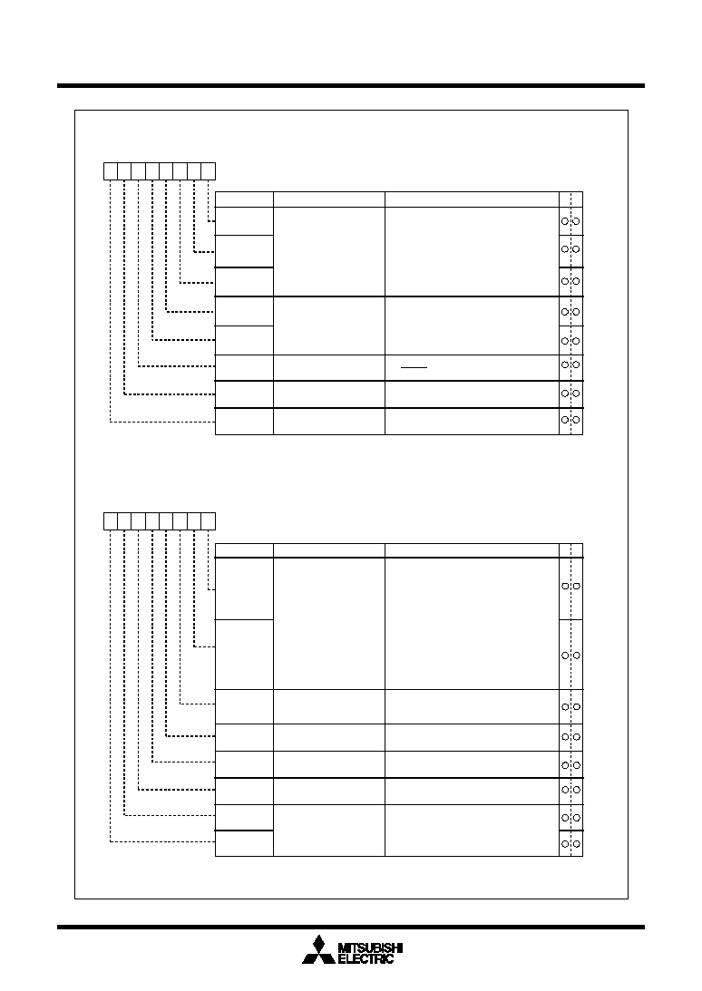
Mitsubishi microcomputers
M16C / 62A Group
SINGLE-CHIP 16-BIT CMOS MICROCOMPUTER
A-D Converter
150
Figure 1.17.2. A-D converter-related registers (1)
A-D control register 0 (Note 1)
Symbol
Address
When reset
ADCON0
03D6
16
00000XXX
2
b7
b6
b5
b4
b3
b2
b1
b0
Analog input pin select bit
0 0 0 : AN
0
is selected
0 0 1 : AN
1
is selected
0 1 0 : AN
2
is selected
0 1 1 : AN
3
is selected
1 0 0 : AN
4
is selected
1 0 1 : AN
5
is selected
1 1 0 : AN
6
is selected
1 1 1 : AN
7
is selected
(Note 2)
CH0
Bit symbol
Bit name
Function
CH1
CH2
A-D operation mode
select bit 0
0 0 : One-shot mode
0 1 : Repeat mode
1 0 : Single sweep mode
1 1 : Repeat sweep mode 0
Repeat sweep mode 1
(Note 2)
MD0
MD1
Trigger select bit
0 : Software trigger
1 : AD
TRG
trigger
TRG
ADST
A-D conversion start flag
0 : A-D conversion disabled
1 : A-D conversion started
Frequency select bit 0
0 : f
AD
/4 is selected
1 : f
AD
/2 is selected
CKS0
W
R
A-D control register 1 (Note)
Symbol Address
When
reset
ADCON1
03D7
16
00
16
Bit name
Function
Bit symbol
b7
b6
b5
b4
b3
b2
b1
b0
A-D sweep pin select bit
SCAN0
SCAN1
MD2
BITS
8/10-bit mode select bit
0 : 8-bit mode
1 : 10-bit mode
VCUT
OPA0
Vref connect bit
OPA1
A-D operation mode
select bit 1
0 : Any mode other than repeat sweep
mode 1
1 : Repeat sweep mode 1
0 : Vref not connected
1 : Vref connected
External op-amp
connection mode bit
W
R
b2 b1 b0
b4 b3
When single sweep and repeat sweep
mode 0 are selected
0 0 : AN
0
, AN
1
(2 pins)
0 1 : AN
0
to AN
3
(4 pins)
1 0 : AN
0
to AN
5
(6 pins)
1 1 : AN
0
to AN
7
(8 pins)
b1 b0
When repeat sweep mode 1 is selected
0 0 : AN
0
(1 pin)
0 1 : AN
0
, AN
1
(2 pins)
1 0 : AN
0
to AN
2
(3 pins)
1 1 : AN
0
to AN
3
(4 pins)
b1 b0
0 0 : ANEX0 and ANEX1 are not used
0 1 : ANEX0 input is A-D converted
1 0 : ANEX1 input is A-D converted
1 1 : External op-amp connection mode
b7 b6
Note 1: If the A-D control register is rewritten during A-D conversion, the conversion result is
indeterminate.
Note 2: When changing A-D operation mode, set analog input pin again.
Frequency select bit 1
0 : f
AD
/2 or f
AD
/4 is selected
1 : f
AD
is selected
CKS1
Note: If the A-D control register is rewritten during A-D conversion, the conversion result is
indeterminate.

Mitsubishi microcomputers
M16C / 62A Group
SINGLE-CHIP 16-BIT CMOS MICROCOMPUTER
A-D Converter
151
Figure 1.17.3. A-D converter-related registers (2)
A-D control register 2 (Note)
Symbol
Address
When reset
ADCON2
03D4
16
0000XXX0
2
b7
b6
b5
b4
b3
b2
b1
b0
A-D conversion method
select bit
0 : Without sample and hold
1 : With sample and hold
Bit symbol
Bit name
Function
R W
Note: If the A-D control register is rewritten during A-D conversion, the conversion
result is indeterminate.
Nothing is assigned.
In an attempt to write to these bits, write "0". The value, if read, turns out to
be "0".
A-D register i
Symbol
Address
When reset
ADi(i=0 to 7)
03C0
16
to 03CF
16
Indeterminate
Eight low-order bits of A-D conversion result
Function
R W
(b15)
b7
b7
b0
b0
(b8)
∑ During 10-bit mode
Two high-order bits of A-D conversion result
Nothing is assigned.
In an attempt to write to these bits, write "0". The value, if
read, turns out to be "0".
∑ During 8-bit mode
When read, the content is indeterminate
SMP
Reserved bit
Always set to "0"
0 0 0

Mitsubishi microcomputers
M16C / 62A Group
SINGLE-CHIP 16-BIT CMOS MICROCOMPUTER
A-D Converter
152
(1) One-shot mode
In one-shot mode, the pin selected using the analog input pin select bit is used for one-shot A-D conver-
sion. Table 1.17.2 shows the specifications of one-shot mode. Figure 1.17.4 shows the A-D control regis-
ter in one-shot mode.
Table 1.17.2. One-shot mode specifications
Figure 1.17.4. A-D conversion register in one-shot mode
A-D control register 0 (Note 1)
Symbol
Address
When reset
ADCON0
03D6
16
00000XXX
2
b7
b6
b5
b4
b3
b2
b1
b0
Analog input pin select
bit
Bit symbol
Bit name
Function
CH1
CH2
A-D operation mode
select bit 0
MD0
MD1
Trigger select bit
0 : Software trigger
1 : AD
TRG
trigger
TRG
ADST
A-D conversion start flag
0 : A-D conversion disabled
1 : A-D conversion started
Frequency select bit 0
0: f
AD
/4 is selected
1: f
AD
/2 is selected
CKS0
W
R
0
0
A-D control register 1 (Note)
Symbol
Address
When reset
ADCON1
03D7
16
00
16
Bit name
Function
Bit symbol
b7
b6
b5
b4
b3
b2
b1
b0
A-D sweep pin
select bit
SCAN0
SCAN1
MD2
BITS
8/10-bit mode select bit
0 : 8-bit mode
1 : 10-bit mode
VCUT
OPA0
Vref connect bit
OPA1
A-D operation mode
select bit 1
Set to "0" when this mode is selected
1 : Vref connected
External op-amp
connection mode bit
0 0 : ANEX0 and ANEX1 are not used
0 1 : ANEX0 input is A-D converted
1 0 : ANEX1 input is A-D converted
1 1 : External op-amp connection mode
W
R
Invalid in one-shot mode
0
0 0 0 : AN
0
is selected
0 0 1 : AN
1
is selected
0 1 0 : AN
2
is selected
0 1 1 : AN
3
is selected
1 0 0 : AN
4
is selected
1 0 1 : AN
5
is selected
1 1 0 : AN
6
is selected
1 1 1 : AN
7
is selected
(Note 2)
b2 b1 b0
0 0 : One-shot mode
(Note 2)
b4 b3
CH0
b7 b6
1
Note 1: If the A-D control register is rewritten during A-D conversion, the conversion
result is indeterminate.
Note 2: When changing A-D operation mode, set analog input pin again.
Frequency select bit1
0 : f
AD
/2 or f
AD
/4 is selected
1 : f
AD
is selected
CKS1
Note: If the A-D control register is rewritten during A-D conversion, the conversion
result is indeterminate.
Item
Specification
Function
The pin selected by the analog input pin select bit is used for one A-D conversion
Start condition
Writing "1" to A-D conversion start flag
Stop condition
∑ End of A-D conversion (A-D conversion start flag changes to "0", except
when external trigger is selected)
∑ Writing "0" to A-D conversion start flag
Interrupt request generation timing
End of A-D conversion
Input pin
One of AN
0
to AN
7
, as selected
Reading of result of A-D converter
Read A-D register corresponding to selected pin

Mitsubishi microcomputers
M16C / 62A Group
SINGLE-CHIP 16-BIT CMOS MICROCOMPUTER
A-D Converter
153
(2) Repeat mode
In repeat mode, the pin selected using the analog input pin select bit is used for repeated A-D conversion.
Table 1.17.3 shows the specifications of repeat mode. Figure 1.17.5 shows the A-D control register in
repeat mode.
A-D control register 0 (Note 1)
Symbol
Address When
reset
ADCON0
03D6
16
00000XXX
2
b7
b6
b5
b4
b3
b2
b1
b0
Analog input pin
select bit
CH0
Bit symbol
Bit name
Function
CH1
CH2
A-D operation mode
select bit 0
MD0
MD1
Trigger select bit
0 : Software trigger
1 : AD
TRG
trigger
TRG
ADST
A-D conversion start flag
0 : A-D conversion disabled
1 : A-D conversion started
Frequency select bit 0
0 : f
AD
/4 is selected
1 : f
AD
/2 is selected
CKS0
W
R
A-D control register 1 (Note)
Symbol
Address
When reset
ADCON1
03D7
16
00
16
Bit name
Function
Bit symbol
b7
b6
b5
b4
b3
b2
b1
b0
A-D sweep pin
select bit
SCAN0
SCAN1
MD2
BITS
8/10-bit mode select bit
0 : 8-bit mode
1 : 10-bit mode
VCUT
OPA0
Vref connect bit
OPA1
A-D operation mode
select bit 1
1 : Vref connected
External op-amp
connection mode bit
W
R
0
1
Invalid in repeat mode
0
0 0 0 : AN
0
is selected
0 0 1 : AN
1
is selected
0 1 0 : AN
2
is selected
0 1 1 : AN
3
is selected
1 0 0 : AN
4
is selected
1 0 1 : AN
5
is selected
1 1 0 : AN
6
is selected
1 1 1 : AN
7
is selected
(Note 2)
b2 b1 b0
0 1 : Repeat mode
(Note 2)
b4 b3
0 0 : ANEX0 and ANEX1 are not used
0 1 : ANEX0 input is A-D converted
1 0 : ANEX1 input is A-D converted
1 1 : External op-amp connection mode
b7 b6
1
Note 1: If the A-D control register is rewritten during A-D conversion, the conversion
result is indeterminate.
Note 2: When changing A-D operation mode, set analog input pin again.
Frequency select bit 1
0 : f
AD
/2 or f
AD
/4 is selected
1 : f
AD
is selected
CKS1
Note: If the A-D control register is rewritten during A-D conversion, the conversion
result is indeterminate.
Set to "0" when this mode is selected
Figure 1.17.5. A-D conversion register in repeat mode
Item
Specification
Function
The pin selected by the analog input pin select bit is used for repeated A-D conversion
Star condition
Writing "1" to A-D conversion start flag
Stop condition
Writing "0" to A-D conversion start flag
Interrupt request generation timing
None generated
Input pin
One of AN
0
to AN
7
, as selected
Reading of result of A-D converter
Read A-D register corresponding to selected pin (at any time)
Table 1.17.3. Repeat mode specifications

Mitsubishi microcomputers
M16C / 62A Group
SINGLE-CHIP 16-BIT CMOS MICROCOMPUTER
A-D Converter
154
(3) Single sweep mode
In single sweep mode, the pins selected using the A-D sweep pin select bit are used for one-by-one A-D
conversion. Table 1.17.4 shows the specifications of single sweep mode. Figure 1.17.6 shows the A-D
control register in single sweep mode.
Table 1.17.4. Single sweep mode specifications
Figure 1.17.6. A-D conversion register in single sweep mode
A-D control register 0 (Note)
Symbol
Address
When reset
ADCON0
03D6
16
00000XXX
2
b7
b6
b5
b4
b3
b2
b1
b0
Analog input pin
select bit
CH0
Bit symbol
Bit name
Function
CH1
CH2
A-D operation mode
select bit 0
1 0 : Single sweep mode
MD0
MD1
Trigger select bit
0 : Software trigger
1 : AD
TRG
trigger
TRG
ADST
A-D conversion start flag
0 : A-D conversion disabled
1 : A-D conversion started
Frequency select bit 0
0 : f
AD
/4 is selected
1 : f
AD
/2 is selected
CKS0
W
R
A-D control register 1 (Note 1)
Symbol
Address
When reset
ADCON1
03D7
16
00
16
Bit name
Function
Bit symbol
b7
b6
b5
b4
b3
b2
b1
b0
A-D sweep pin select bit
SCAN0
SCAN1
MD2
BITS
8/10-bit mode select bit
0 : 8-bit mode
1 : 10-bit mode
VCUT
OPA0
Vref connect bit
OPA1
A-D operation mode
select bit 1
1 : Vref connected
External op-amp
connection mode
bit (Note 2)
W
R
1 0
Invalid in single sweep mode
0
Note 1: If the A-D control register is rewritten during A-D conversion, the conversion result
is indeterminate.
Note 2: Neither `01' nor `10' can be selected with the external op-amp connection mode bit.
b4 b3
When single sweep and repeat sweep mode 0
are selected
0 0 : AN
0
, AN
1
(2 pins)
0 1 : AN
0
to AN
3
(4 pins)
1 0 : AN
0
to AN
5
(6 pins)
1 1 : AN
0
to AN
7
(8 pins)
b1 b0
0 0 : ANEX0 and ANEX1 are not used
0 1 : ANEX0 input is A-D converted
1 0 : ANEX1 input is A-D converted
1 1 : External op-amp connection mode
b7 b6
1
Note: If the A-D control register is rewritten during A-D conversion, the conversion result
is indeterminate.
Frequency select bit 1
0 : f
AD
/2 or f
AD
/4 is selected
1 : f
AD
is selected
CKS1
Set to "0" when this mode is selected
Item
Specification
Function
The pins selected by the A-D sweep pin select bit are used for one-by-one A-D conversion
Start condition
Writing "1" to A-D converter start flag
Stop condition
∑ End of A-D conversion (A-D conversion start flag changes to "0", except
when external trigger is selected)
∑ Writing "0" to A-D conversion start flag
Interrupt request generation timing
End of A-D conversion
Input pin
AN
0
and AN
1
(2 pins), AN
0
to AN
3
(4 pins), AN
0
to AN
5
(6 pins), or AN
0
to AN
7
(8 pins)
Reading of result of A-D converter
Read A-D register corresponding to selected pin

Mitsubishi microcomputers
M16C / 62A Group
SINGLE-CHIP 16-BIT CMOS MICROCOMPUTER
A-D Converter
155
(4) Repeat sweep mode 0
In repeat sweep mode 0, the pins selected using the A-D sweep pin select bit are used for repeat sweep
A-D conversion. Table 1.17.5 shows the specifications of repeat sweep mode 0. Figure 1.17.7 shows the
A-D control register in repeat sweep mode 0.
Figure 1.17.7. A-D conversion register in repeat sweep mode 0
A-D control register 0 (Note)
Symbol
Address
When reset
ADCON0
03D6
16
00000XXX
2
b7
b6
b5
b4
b3
b2
b1
b0
Analog input pin
select bit
CH0
Bit symbol
Bit name
Function
CH1
CH2
A-D operation mode
select bit 0
1 1 : Repeat sweep mode 0
MD0
MD1
Trigger select bit
0 : Software trigger
1 : AD
TRG
trigger
TRG
ADST
A-D conversion start flag
0 : A-D conversion disabled
1 : A-D conversion started
Frequency select bit 0
0 : f
AD
/4 is selected
1 : f
AD
/2 is selected
CKS0
W
R
A-D control register 1 (Note 1)
Symbol
Address
When reset
ADCON1
03D7
16
00
16
Bit name
Function
Bit symbol
b7
b6
b5
b4
b3
b2
b1
b0
A-D sweep pin select bit
SCAN0
SCAN1
MD2
BITS
8/10-bit mode select bit
0 : 8-bit mode
1 : 10-bit mode
VCUT
OPA0
Vref connect bit
OPA1
A-D operation mode
select bit 1
1 : Vref connected
External op-amp
connection mode
bit (Note 2)
W
R
1 1
Invalid in repeat sweep mode 0
0
Note 1: If the A-D control register is rewritten during A-D conversion, the conversion result
is indeterminate.
Note 2: Neither "01" nor "10" can be selected with the external op-amp connection mode bit.
b4 b3
When single sweep and repeat sweep mode 0
are selected
0 0 : AN
0
, AN
1
(2 pins)
0 1 : AN
0
to AN
3
(4 pins)
1 0 : AN
0
to AN
5
(6 pins)
1 1 : AN
0
to AN
7
(8 pins)
b1 b0
0 0 : ANEX0 and ANEX1 are not used
0 1 : ANEX0 input is A-D converted
1 0 : ANEX1 input is A-D converted
1 1 : External op-amp connection mode
b7 b6
1
Note: If the A-D control register is rewritten during A-D conversion, the conversion result
is indeterminate.
Frequency select bit 1
0 : f
AD
/2 or f
AD
/4 is selected
1 : f
AD
is selected
CKS1
Set to "0" when this mode is selected
Item
Specification
Function
The pins selected by the A-D sweep pin select bit are used for repeat A-D conversion
Start condition
Writing "1" to A-D conversion start flag
Stop condition
Writing "0" to A-D conversion start flag
Interrupt request generation timing
None generated
Input pin
AN
0
and AN
1
(2 pins), AN
0
to AN
3
(4 pins), AN
0
to AN
5
(6 pins), or AN
0
to AN
7
(8 pins)
Reading of result of A-D converter
Read A-D register corresponding to selected pin (at any time)
Table 1.17.5. Repeat sweep mode 0 specifications

Mitsubishi microcomputers
M16C / 62A Group
SINGLE-CHIP 16-BIT CMOS MICROCOMPUTER
A-D Converter
156
Item
Specification
Function
All pins perform repeat A-D conversion, with emphasis on the pin or pins
selected by the A-D sweep pin select bit
Example : AN
0
selected AN
0
AN
1
AN
0
AN
2
AN
0
AN
3
, etc
Start condition
Writing "1" to A-D conversion start flag
Stop condition
Writing "0" to A-D conversion start flag
Interrupt request generation timing
None generated
Input pin
With emphasis on these pins ; AN
0
(1 pin), AN
0
and AN
1
(2 pins),
AN
0
to AN
2
(3 pins), AN
0
to AN
3
(4 pins)
Reading of result of A-D converter
Read A-D register corresponding to selected pin (at any time)
(5) Repeat sweep mode 1
In repeat sweep mode 1, all pins are used for A-D conversion with emphasis on the pin or pins selected
using the A-D sweep pin select bit. Table 1.17.6 shows the specifications of repeat sweep mode 1. Figure
1.17.8 shows the A-D control register in repeat sweep mode 1.
A-D control register 0 (Note)
Symbol
Address
When reset
ADCON0
03D6
16
00000XXX
2
b7
b6
b5
b4
b3
b2
b1
b0
Analog input pin
select bit
CH0
Bit symbol
Bit name
Function
CH1
CH2
A-D operation mode
select bit 0
1 1 : Repeat sweep mode 1
MD0
MD1
Trigger select bit
0 : Software trigger
1 : AD
TRG
trigger
TRG
ADST
A-D conversion start flag
0 : A-D conversion disabled
1 : A-D conversion started
Frequency select bit 0
0 : f
AD
/4 is selected
1 : f
AD
/2 is selected
CKS0
W
R
A-D control register 1 (Note 1)
Symbol
Address
When reset
ADCON1
03D7
16
00
16
Bit name
Function
Bit symbol
b7
b6
b5
b4
b3
b2
b1
b0
A-D sweep pin select bit
SCAN0
SCAN1
MD2
BITS
8/10-bit mode select bit
0 : 8-bit mode
1 : 10-bit mode
VCUT
OPA0
Vref connect bit
OPA1
A-D operation mode
select bit 1
1 : Vref connected
External op-amp
connection mode
bit (Note 2)
W
R
1 1
Invalid in repeat sweep mode 1
1
Note 1: If the A-D control register is rewritten during A-D conversion, the conversion result
is indeterminate.
Note 2: Neither `01' nor `10' can be selected with the external op-amp connection mode bit.
b4 b3
When repeat sweep mode 1 is selected
0 0 : AN
0
(1 pin)
0 1 : AN
0
, AN
1
(2 pins)
1 0 : AN
0
to AN
2
(3 pins)
1 1 : AN
0
to AN
3
(4 pins)
b1 b0
0 0 : ANEX0 and ANEX1 are not used
0 1 : ANEX0 input is A-D converted
1 0 : ANEX1 input is A-D converted
1 1 : External op-amp connection mode
b7 b6
1
Note: If the A-D control register is rewritten during A-D conversion, the conversion result
is indeterminate.
Frequency select bit 1
0 : f
AD
/2 or f
AD
/4 is selected
1 : f
AD
is selected
CKS1
Set to "1" when this mode is selected
Figure 1.17.8. A-D conversion register in repeat sweep mode 1
Table 1.17.6. Repeat sweep mode 1 specifications
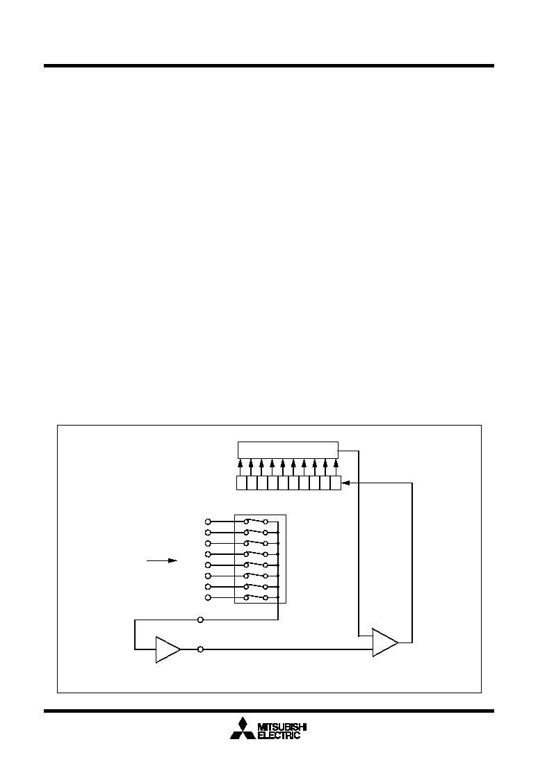
Mitsubishi microcomputers
M16C / 62A Group
SINGLE-CHIP 16-BIT CMOS MICROCOMPUTER
A-D Converter
157
(a) Sample and hold
Sample and hold is selected by setting bit 0 of the A-D control register 2 (address 03D4
16
) to "1". When
sample and hold is selected, the rate of conversion of each pin increases. As a result, a 28
AD
cycle is
achieved with 8-bit resolution and 33
AD
with 10-bit resolution. Sample and hold can be selected in all
modes. However, in all modes, be sure to specify before starting A-D conversion whether sample and
hold is to be used.
(b) Extended analog input pins
In one-shot mode and repeat mode, the input via the extended analog input pins ANEX0 and ANEX1 can
also be converted from analog to digital.
When bit 6 of the A-D control register 1 (address 03D7
16
) is "1" and bit 7 is "0", input via ANEX0 is
converted from analog to digital. The result of conversion is stored in A-D register 0.
When bit 6 of the A-D control register 1 (address 03D7
16
) is "0" and bit 7 is "1", input via ANEX1 is
converted from analog to digital. The result of conversion is stored in A-D register 1.
(c) External operation amp connection mode
In this mode, multiple external analog inputs via the extended analog input pins, ANEX0 and ANEX1, can
be amplified together by just one operation amp and used as the input for A-D conversion.
When bit 6 of the A-D control register 1 (address 03D7
16
) is "1" and bit 7 is "1", input via AN
0
to AN
7
is
output from ANEX0. The input from ANEX1 is converted from analog to digital and the result stored in the
corresponding A-D register. The speed of A-D conversion depends on the response of the external op-
eration amp. Do not connect the ANEX0 and ANEX1 pins directly. Figure 1.17.9 is an example of how to
connect the pins in external operation amp mode.
Analog
input
External op-amp
AN
0
AN
7
AN
1
AN
2
AN
3
AN
4
AN
5
AN
6
ANEX1
ANEX0
Resistor ladder
Successive conversion register
Comparator
Figure 1.17.9. Example of external op-amp connection mode

Mitsubishi microcomputers
M16C / 62A Group
SINGLE-CHIP 16-BIT CMOS MICROCOMPUTER
D-A Converter
158
D-A Converter
This is an 8-bit, R-2R type D-A converter. The microcomputer contains two independent D-A converters of
this type.
D-A conversion is performed when a value is written to the corresponding D-A register. Bits 0 and 1 (D-A
output enable bits) of the D-A control register decide if the result of conversion is to be output. Do not set the
target port to output mode if D-A conversion is to be performed. When the D-A output is enabled, the pull-
up function of the corresponding port is automatically disabled.
Output analog voltage (V) is determined by a set value (n : decimal) in the D-A register.
V = V
REF
X n/ 256 (n = 0 to 255)
V
REF
: reference voltage
Table 1.18.1 lists the performance of the D-A converter. Figure 1.18.1 shows the block diagram of the D-A
converter. Figure 1.18.2 shows the D-A control register. Figure 1.18.3 shows the D-A converter equivalent
circuit.
Item
Performance
Conversion method
R-2R method
Resolution
8 bits
Analog output pin
2 channels
Table 1.18.1. Performance of D-A converter
P9
3
/DA
0
P9
4
/DA
1
Data bus low-order bits
D-A register 0 (8)
R-2R resistor ladder
D-A0 output enable bit
D-A register 1 (8)
R-2R resistor ladder
D-A1 output enable bit
(Address 03D8
16
)
(Address 03DA
16
)
Figure 1.18.1. Block diagram of D-A converter

Mitsubishi microcomputers
M16C / 62A Group
SINGLE-CHIP 16-BIT CMOS MICROCOMPUTER
D-A Converter
159
Figure 1.18.2. D-A control register
D-A control register
Symbol
Address
When reset
DACON
03DC
16
00
16
b7
b6
b5
b4
b3
b2
b1
b0
D-A0 output enable bit
DA0E
Bit symbol
Bit name
Function
R W
0 : Output disabled
1 : Output enabled
D-A1 output enable bit
0 : Output disabled
1 : Output enabled
DA1E
Nothing is assigned.
In an attempt to write to these bits, write "0". The value, if read, turns out to be "0"
D-A register
Symbol
Address
When reset
DAi (i = 0,1)
03D8
16
,
03DA
16
Indeterminate
W
R
b7
b0
Function
R W
Output value of D-A conversion
V
REF
AV
SS
2R
R
2R
R
2R
R
2R
R
2R
R
2R
R
2R
R
2R
2R
DA0
MSB
LSB
D-A0 output enable bit
"0"
"1"
D-A register 0
Note 1: The above diagram shows an instance in which the D-A register is assigned 2A
16
.
Note 2: The same circuit as this is also used for D-A1.
Note 3: To reduce the current consumption when the D-A converter is not used, set the D-A output enable bit to 0 and set the D-A register to 00
16
so that no current flows in the resistors Rs and 2Rs.
"0"
"1"
Figure 1.18.3. D-A converter equivalent circuit

Mitsubishi microcomputers
M16C / 62A Group
SINGLE-CHIP 16-BIT CMOS MICROCOMPUTER
CRC
160
CRC Calculation Circuit
The Cyclic Redundancy Check (CRC) calculation circuit detects an error in data blocks. The microcom-
puter uses a generator polynomial of CRC_CCITT (X
16
+ X
12
+ X
5
+ 1) to generate CRC code.
The CRC code is a 16-bit code generated for a block of a given data length in multiples of 8 bits. The CRC
code is set in a CRC data register each time one byte of data is transferred to a CRC input register after
writing an initial value into the CRC data register. Generation of CRC code for one byte of data is com-
pleted in two machine cycles.
Figure 1.19.1 shows the block diagram of the CRC circuit. Figure 1.19.2 shows the CRC-related registers.
Figure 1.19.3 shows the calculation example using the CRC calculation circuit.
Figure 1.19.2. CRC-related registers
Symbol
Address
When reset
CRCD
03BD
16
, 03BC
16
Indeterminate
b7
b0 b7
b0
(b15)
(b8)
CRC data register
W
R
CRC calculation result output register
Function
Values that
can be set
0000
16
to FFFF
16
Symbo
Address
When reset
CRCIN
03BE
16
Indeterminate
b7
b0
CRC input register
W
R
Data input register
Function
Values that
can be set
00
16
to FF
16
Eight low-order bits
Eight high-order bits
Data bus high-order bits
Data bus low-order bits
CRC data register (16)
CRC input register (8)
CRC code generating circuit
x
16
+ x
12
+ x
5
+ 1
(Addresses 03BD
16
, 03BC
16
)
(Address 03BE
16
)
Figure 1.19.1. Block diagram of CRC circuit

Mitsubishi microcomputers
M16C / 62A Group
SINGLE-CHIP 16-BIT CMOS MICROCOMPUTER
CRC
161
b15
b0
(1) Setting 0000
16
CRC data register
CRCD
[03BD
16
, 03BC
16
]
b0
b7
b15
b0
(2) Setting 01
16
CRC input register
CRCIN
[03BE
16
]
2 cycles
After CRC calculation is complete
CRC data register
CRCD
[03BD
16
, 03BC
16
]
1189
16
Stores CRC code
b0
b7
b15
b0
(3) Setting 23
16
CRC input register
CRCIN
[03BE
16
]
After CRC calculation is complete
CRC data register
CRCD
[03BD
16
, 03BC
16
]
0A41
16
Stores CRC code
The code resulting from sending 01
16
in LSB first mode is (1000 0000). Thus the CRC code in the generating polynomial,
(X
16
+ X
12
+ X
5
+ 1), becomes the remainder resulting from dividing (1000 0000) X
16
by (1 0001 0000 0010 0001) in
conformity with the modulo-2 operation.
Thus the CRC code becomes (1001 0001 1000 1000). Since the operation is in LSB first mode, the (1001 0001 1000 1000)
corresponds to 1189
16
in hexadecimal notation. If the CRC operation in MSB first mode is necessary in the CRC operation
circuit built in the M16C, switch between the LSB side and the MSB side of the input-holding bits, and carry out the CRC
operation. Also switch between the MSB and LSB of the result as stored in CRC data.
1 0001 0000 0010 0001
1000 0000 0000 0000 0000 0000
1000 1000 0001 0000 1
1000 0001 0000 1000 0
1000 1000 0001 0000 1
1001 0001 1000 1000
1000 1000
LSB
MSB
LSB
MSB
9
8
1
1
Modulo-2 operation is
operation that complies
with the law given below.
0 + 0 = 0
0 + 1 = 1
1 + 0 = 1
1 + 1 = 0
-1 = 1
Figure 1.19.3. Calculation example using the CRC calculation circuit

Mitsubishi microcomputers
M16C / 62A Group
SINGLE-CHIP 16-BIT CMOS MICROCOMPUTER
Programmable I/O Port
162
Programmable I/O Ports
There are 87 programmable I/O ports: P0 to P10 (excluding P8
5
). Each port can be set independently for
input or output using the direction register. A pull-up resistance for each block of 4 ports can be set. P8
5
is
an input-only port and has no built-in pull-up resistance.
Figures 1.20.1 to 1.20.4 show the programmable I/O ports. Figure 1.20.5 shows the I/O pins.
Each pin functions as a programmable I/O port and as the I/O for the built-in peripheral devices.
To use the pins as the inputs for the built-in peripheral devices, set the direction register of each pin to input
mode. When the pins are used as the outputs for the built-in peripheral devices (other than the D-A con-
verter), they function as outputs regardless of the contents of the direction registers. When pins are to be
used as the outputs for the D-A converter, do not set the direction registers to output mode. See the
descriptions of the respective functions for how to set up the built-in peripheral devices.
(1) Direction registers
Figure 1.20.6 shows the direction registers.
These registers are used to choose the direction of the programmable I/O ports. Each bit in these regis-
ters corresponds one for one to each I/O pin.
In memory expansion and microprocessor mode, the contents of corresponding direction register of pins
_______
_______
_____
________ ______
________ _______
_______
__________
_________
A
0
to A
19
, D
0
to D
15
, CS0 to CS3, RD, WRL/WR, WRH/BHE, ALE, RDY, HOLD, HLDA and BCLK cannot
be modified.
Note: There is no direction register bit for P8
5
.
(2) Port registers
Figure 1.20.7 shows the port registers.
These registers are used to write and read data for input and output to and from an external device. A
port register consists of a port latch to hold output data and a circuit to read the status of a pin. Each bit
in port registers corresponds one for one to each I/O pin.
In memory expansion and microprocessor mode, the contents of corresponding port register of pins A
0
to
_______
________ _____
________ ______
________ ________
_______
__________
_________
A
19
, D
0
to D
15
, CS0 to CS3, RD, WRL/WR, WRH/BHE, ALE, RDY, HOLD, HLDA and BCLK cannot be
modified.
(3) Pull-up control registers
Figure 1.20.8 shows the pull-up control registers.
The pull-up control register can be set to apply a pull-up resistance to each block of 4 ports. When ports
are set to have a pull-up resistance, the pull-up resistance is connected only when the direction register is
set for input.
However, in memory expansion mode and microprocessor mode, the pull-up control register of P0 to P3,
P4
0
to P4
3
, and P5 is invalid. The contents of register can be changed, but the pull-up resistance is not
connected.
(4) Port control register
Figure 1.20.9 shows the port control register.
The bit 0 of port control register is used to read port P1 as follows:
0 : When port P1 is input port, port input level is read.
When port P1 is output port , the contents of port P1 register is read.
1 : The contents of port P1 register is read always.
This register is valid in the following:
∑ External bus width is 8 bits in microprocessor mode or memory expansion mode.
∑ Port P1 can be used as a port in multiplexed bus for the entire space.

Mitsubishi microcomputers
M16C / 62A Group
SINGLE-CHIP 16-BIT CMOS MICROCOMPUTER
Programmable I/O Port
163
Figure 1.20.1. Programmable I/O ports (1)
P0
0
to P0
7
, P2
0
to P2
7
,
P3
0
to P3
7
, P4
0
to P4
7
,
P5
0
to P5
4
, P5
6
P1
0
to P1
4
P1
5
to P1
7
P5
7
, P6
0
, P6
1
, P6
4
, P6
5
,
P7
2
to P7
6
, P8
0
, P8
1
,
P9
0
, P9
2
Data bus
Direction register
Pull-up selection
Port latch
Data bus
Direction register
Pull-up selection
Port latch
Port P1 control register
Direction register
Port latch
Port P1 control register
Pull-up selection
Data bus
Input to respective peripheral functions
Direction register
Port latch
Pull-up selection
Data bus
Input to respective peripheral functions
Note :1 symbolizes a parasitic diode.
Do not apply a voltage higher than Vcc to each port.
"1"
Output
(Note)
(Note)
(Note)
(Note)

Mitsubishi microcomputers
M16C / 62A Group
SINGLE-CHIP 16-BIT CMOS MICROCOMPUTER
Programmable I/O Port
164
Figure 1.20.2. Programmable I/O ports (2)
P7
0
, P7
1
P8
5
P8
2
to P8
4
P5
5
, P6
2
, P6
6
, P7
7
,
P9
1
, P9
7
P6
3
, P6
7
Data bus
Direction register
Pull-up selection
Port latch
Input to respective peripheral functions
Data bus
Direction register
Pull-up selection
Port latch
Input to respective peripheral functions
"1"
Output
Data bus
Direction register
Pull-up selection
Port latch
Data bus
NMI interrupt input
"1"
Output
Direction register
Port latch
Input to respective peripheral functions
Note :1 symbolizes a parasitic diode.
Do not apply a voltage higher than Vcc to each port.
Note :2 symbolizes a parasitic diode.
(Note1)
(Note1)
(Note1)
(Note1)
(Note2)
Data bus
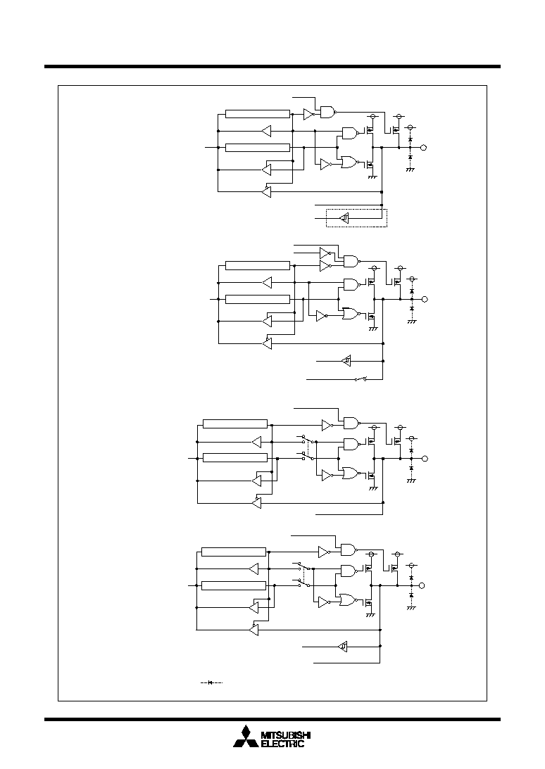
Mitsubishi microcomputers
M16C / 62A Group
SINGLE-CHIP 16-BIT CMOS MICROCOMPUTER
Programmable I/O Port
165
Figure 1.20.3. Programmable I/O ports (3)
P9
3
, P9
4
P9
6
P9
5
Data bus
Direction register
Pull-up selection
Port latch
Analog input
Input to respective peripheral functions
P10
0
to P10
3
(inside dotted-line not included)
P10
4
to P10
7
(inside dotted-line included)
D-A output enabled
Direction register
Pull-up selection
Port latch
Data bus
Input to respective peripheral functions
D-A output enabled
Analog output
"1"
Output
Direction register
Pull-up selection
Port latch
Data bus
Analog input
"1"
Output
Direction register
Pull-up selection
Port latch
Data bus
Analog input
Input to respective peripheral functions
Note : symbolizes a parasitic diode.
Do not apply a voltage higher than Vcc to each port.
(Note)
(Note)
(Note)
(Note)

Mitsubishi microcomputers
M16C / 62A Group
SINGLE-CHIP 16-BIT CMOS MICROCOMPUTER
Programmable I/O Port
166
Figure 1.20.5. I/O pins
Figure 1.20.4. Programmable I/O ports (4)
P8
7
P8
6
fc
Rf
Rd
Data bus
Direction register
Pull-up selection
Port latch
"1"
Output
Direction register
Pull-up selection
Port latch
Data bus
Note : symbolizes a parasitic diode.
Do not apply a voltage higher than Vcc to each port.
(Note)
(Note)
BYTE
BYTE signal input
CNV
SS
CNV
SS
signal input
RESET
RESET signal input
Note 1: symbolizes a parasitic diode.
Do not apply a voltage higher than Vcc to each pin.
Note 2: A parasitic diode on the V
CC
side is added to the mask ROM version.
Do not apply a voltage higher than Vcc to each pin.
(Note 2)
(Note 1)
(Note 2)
(Note 1)
(Note 1)

Mitsubishi microcomputers
M16C / 62A Group
SINGLE-CHIP 16-BIT CMOS MICROCOMPUTER
Programmable I/O Port
167
Figure 1.20.6. Direction register
Port Pi direction register (Note 1, 2)
Symbol
Address
When reset
PDi (i = 0 to 10, except 8)
03E2
16
, 03E3
16
, 03E6
16
, 03E7
16
, 03EA
16
00
16
03EB
16
, 03EE
16
, 03EF
16
, 03F3
16
, 03F6
16
Bit name
Function
Bit symbol
W
R
b7
b6
b5
b4
b3
b2
b1
b0
PDi_0
Port Pi
0
direction register
PDi_1
Port Pi
1
direction register
PDi_2
Port Pi
2
direction register
PDi_3
Port Pi
3
direction register
PDi_4
Port Pi
4
direction register
PDi_5
Port Pi
5
direction register
PDi_6
Port Pi
6
direction register
PDi_7
Port Pi
7
direction register
0 : Input mode
(Functions as an input port)
1 : Output mode
(Functions as an output port)
(i = 0 to 10 except 8)
Port P8 direction register
Symbol
Address
When reset
PD8
03F2
16
00X00000
2
Bit name
Function
Bit symbol
W
R
b7
b6
b5
b4
b3
b2
b1
b0
PD8_0
Port P8
0
direction register
PD8_1
Port P8
1
direction register
PD8_2
Port P8
2
direction register
PD8_3
Port P8
3
direction register
PD8_4
Port P8
4
direction register
Nothing is assigned.
In an attempt to write to this bit, write "0". The value, if read, turns out to be
indeterminate.
PD8_6
Port P8
6
direction register
PD8_7
Port P8
7
direction register
0 : Input mode
(Functions as an input port)
1 : Output mode
(Functions as an output port)
0 : Input mode
(Functions as an input port)
1 : Output mode
(Functions as an output port)
Note 2: In memory expansion and microprocessor mode, the contents of
corresponding port Pi direction register of pins A
0
to A
19
, D
0
to D
15
,
CS
0
to CS
3
, RD, WRL/WR, WRH/BHE, ALE, RDY, HOLD, HLDA and
BCLK cannot be modified.
Note 1: Set bit 2 of protect register (address 000A
16
) to "1" before rewriting to
the port P9 direction register.

Mitsubishi microcomputers
M16C / 62A Group
SINGLE-CHIP 16-BIT CMOS MICROCOMPUTER
Programmable I/O Port
168
Port Pi register (Note 2)
Symbol
Address
When reset
Pi (i = 0 to 10, except 8)
03E0
16
, 03E1
16
, 03E4
16
, 03E5
16
, 03E8
16
Indeterminate
03E9
16
, 03EC
16
, 03ED
16
, 03F1
16
, 03F4
16
Indeterminate
Bit name
Function
Bit symbol
W
R
b7
b6
b5
b4
b3
b2
b1
b0
Pi_0
Port Pi
0
register
Pi_1
Port Pi
1
register
Pi_2
Port Pi
2
register
Pi_3
Port Pi
3
register
Pi_4
Port Pi
4
register
Pi_5
Port Pi
5
register
Pi_6
Port Pi
6
register
Pi_7
Port Pi
7
register
Data is input and output to and from
each pin by reading and writing to
and from each corresponding bit
0 : "L" level data
1 : "H" level data (Note 1)
(i = 0 to 10 except 8)
Port P8 register
Symbol
Address
When reset
P8
03F0
16
Indeterminate
Bit name
Function
Bit symbol
W
R
b7
b6
b5
b4
b3
b2
b1
b0
P8_0
Port P8
0
register
P8_1
Port P8
1
register
P8_2
Port P8
2
register
P8_3
Port P8
3
register
P8_4
Port P8
4
register
P8_5
Port P8
5
register
P8_6
Port P8
6
register
P8_7
Port P8
7
register
Data is input and output to and from
each pin by reading and writing to
and from each corresponding bit
(except for P8
5
)
0 : "L" level data
1 : "H" level data
Note 1:
Since P7
0
and P7
1
are N-channel open drain ports, the data is high-impedance.
Note 2: In memory expansion and microprocessor mode, the contents of
corresponding port Pi register of pins A
0
to A
19
, D
0
to D
15
, CS
0
to CS
3
,
RD, WRL/WR, WRH/BHE, ALE, RDY, HOLD, HLDA and BCLK cannot
be modified.
Figure 1.20.7. Port register

Mitsubishi microcomputers
M16C / 62A Group
SINGLE-CHIP 16-BIT CMOS MICROCOMPUTER
Programmable I/O Port
169
Figure 1.20.8. Pull-up control register
Pull-up control register 0 (Note)
Symbol
Address
When reset
PUR0
03FC
16
00
16
Bit name
Function
Bit symbol
W
R
b7
b6
b5
b4
b3
b2
b1
b0
PU00
P0
0
to P0
3
pull-up
PU01
P0
4
to P0
7
pull-up
PU02
P1
0
to P1
3
pull-up
PU03
P1
4
to P1
7
pull-up
PU04
P2
0
to P2
3
pull-up
PU05
P2
4
to P2
7
pull-up
PU06
P3
0
to P3
3
pull-up
PU07
P3
4
to P3
7
pull-up
The corresponding port is pulled
high with a pull-up resistor
0 : Not pulled high
1 : Pulled high
Pull-up control register 1
Symbol
Address
When reset
PUR1
03FD
16
00
16
(Note 2)
Bit name
Function
Bit symbol
W
R
b7
b6
b5
b4
b3
b2
b1
b0
PU10
P4
0
to P4
3
pull-up (Note 3)
PU11
P4
4
to P4
7
pull-up
PU12
P5
0
to P5
3
pull-up (Note 3)
PU13
P5
4
to P5
7
pull-up
PU14
P6
0
to P6
3
pull-up
PU15
P6
4
to P6
7
pull-up
PU16
P7
2
to P7
3
pull-up (Note 1)
PU17
P7
4
to P7
7
pull-up
The corresponding port is pulled
high with a pull-up resistor
0 : Not pulled high
1 : Pulled high
Note 1: Since P7
0
and P7
1
are N-channel open drain ports, pull-up is not available for them.
Note 2: When the V
CC
level is being impressed to the CNV
SS
terminal, this register becomes
to 02
16
when reset (PU11 becomes to "1").
Pull-up control register 2
Symbol
Address
When reset
PUR2
03FE
16
00
16
Bit name
Function
Bit symbol
W
R
b7
b6
b5
b4
b3
b2
b1
b0
PU20
P8
0
to P8
3
pull-up
PU21
P8
4
to P8
7
pull-up
(Except P8
5
)
PU22
P9
0
to P9
3
pull-up
PU23
P9
4
to P9
7
pull-up
PU24
P10
0
to P10
3
pull-up
PU25
P10
4
to P10
7
pull-up
Nothing is assigned.
In an attempt to write to these bits, write "0". The value, if read, turns out to be "0".
The corresponding port is pulled
high with a pull-up resistor
0 : Not pulled high
1 : Pulled high
Note 3: In memory expansion and microprocessor mode, the content of these bits can be
changed, but the pull-up resistance is not connected.
Note : In memory expansion and microprocessor mode, the content of this register
can be changed, but the pull-up resistance is not connected.

Mitsubishi microcomputers
M16C / 62A Group
SINGLE-CHIP 16-BIT CMOS MICROCOMPUTER
Programmable I/O Port
170
Figure 1.20.9. Port control register
Port control register
Symbpl
Address
When reset
PCR
03FF
16
00
16
Bit name
Function
Bit symbol
W
R
b7
b6
b5
b4
b3
b2
b1
b0
PCR0
Port P1 control register
0 : When input port, read port
input level. When output port,
read the contents of port P1
register.
1 : Read the contents of port P1
register though input/output
port.
Nothing is assigned.
In an attempt to write to these bits, write "0". The value, if read, turns
out to be "0".

Mitsubishi microcomputers
M16C / 62A Group
SINGLE-CHIP 16-BIT CMOS MICROCOMPUTER
Programmable I/O Port
171
Pin name
Connection
Ports P0 to P10
(excluding P8
5
)
X
OUT
(Note)
AV
SS
, V
REF
, BYTE
AV
CC
After setting for input mode, connect every pin to V
SS
via a resistor
(pull-down); or after setting for output mode, leave these pins open.
Open
Connect to V
CC
Connect to V
SS
Note: With external clock input to X
IN
pin.
NMI
Connect via resistor to V
CC
(pull-up)
Table 1.20.1. Example connection of unused pins in single-chip mode
Pin name
Connection
Ports P6 to P10
(excluding P8
5
)
AV
SS
, V
REF
AV
CC
After setting for input mode, connect every pin to V
SS
via a resistor
(pull-down); or after setting for output mode, leave these pins open.
Open
Connect to V
CC
Connect to V
SS
Note 1: With external clock input to X
IN
pin.
Note 2: When the BCLK output disable bit (bit 7 at address 0004
16
) is set to "1", connect to V
CC
via a resistor (pull-up).
HOLD, RDY, NMI
Connect via resistor to V
CC
(pull-up)
BHE, ALE, HLDA,
X
OUT
(Note 1), BCLK (Note 2)
P4
5
/ CS1 to P4
7
/ CS3
Set ports to input mode, set output enable bits of CS1 through CS3 to
0, and connect to Vcc via resistors (pull-up).
Figure 1.20.10. Example connection of unused pins
Port P0 to P10 (except for P8
5
)
(Input mode)
∑
∑
∑
(Input mode)
(Output mode)
NMI
X
OUT
AV
CC
BYTE
AV
SS
V
REF
Microcomputer
V
CC
V
SS
In single-chip mode
Port P6 to P10 (except for P8
5
)
(Input mode)
∑
∑
∑
(Input mode)
(Output mode)
NMI
X
OUT
AV
CC
AV
SS
V
REF
Open
Microcomputer
V
CC
V
SS
In memory expansion mode or
in microprocessor mode
HOLD
RDY
ALE
BCLK (Note)
BHE
HLDA
Open
Open
Open
∑
∑
∑
∑
∑
∑
Port P4
5
/ CS1
to P4
7
/ CS3
Note : When the BCLK output disable bit (bit 7 at address 0004
16
) is set to "1", connect to V
CC
via a resistor (pull-up).
Table 1.20.2. Example connection of unused pins in memory expansion mode and microprocessor mode

Mitsubishi microcomputers
M16C / 62A Group
SINGLE-CHIP 16-BIT CMOS MICROCOMPUTER
172
Items to be submitted when ordering masked ROM version
Please submit the following when ordering masked ROM products:
(1) Mask ROM confirmation form
(2) Mark specification sheet
(3) ROM data : Floppy disks *
*: 3.5-inch double-sided high-density disk (IBM format) is required per pattern.

Mitsubishi microcomputers
M16C / 62A Group
SINGLE-CHIP 16-BIT CMOS MICROCOMPUTER
Electrical characteristics
173
Table 1.23.1. Absolute maximum ratings
Note : Specify a product of -40
∞
C to 85
∞
C to use it.
V
REF
, X
IN
X
OUT
V
O
-0.3 to Vcc+0.3
-0.3 to Vcc+0.3
P
d
Topr=25
-0.3 to 6.5
-0.3 to 6.5
V
V
V
V
I
AVcc
Vcc
T
stg
T
opr
mW
V
-65 to 150
300
-20 to 85 / -40 to 85 (Note)
P3
0
to P3
7
, P4
0
to P4
7
, P5
0
to P5
7
,
P6
0
to P6
7
, P7
2
to P7
7
, P8
0
to P8
7
,
P0
0
to P0
7
, P1
0
to P1
7
, P2
0
to P2
7
,
P3
0
to P3
7
,P4
0
to P4
7
, P5
0
to P5
7
,
P6
0
to P6
7
,P7
2
to P7
7
, P8
0
to P8
4,
P0
0
to P0
7
, P1
0
to P1
7
, P2
0
to P2
7
,
RESET,
P9
0
to P9
7
, P10
0
to P10
7
,
P8
6
, P8
7
, P9
0
to P9
7
, P10
0
to P10
7
,
P7
0
, P7
1
P7
0
, P7
1
-0.3 to 6.5
-0.3 to 6.5
V
V
CNV
SS
, BYTE,
V
CC
=AV
CC
V
CC
=AV
CC
C
C
C
Symbol
Parameter
Condition
Rated value
Unit
Supply voltage
Analog supply voltage
Input
voltage
Output
voltage
Power dissipation
Operating ambient temperature
Storage temperature

Mitsubishi microcomputers
M16C / 62A Group
SINGLE-CHIP 16-BIT CMOS MICROCOMPUTER
Electrical characteristics
174
Note 1: The mean output current is the mean value within 100ms.
Note 2: The total I
OL
(peak) for ports P0, P1, P2, P8
6
, P8
7
, P9, and P10 must be 80mA max. The total I
OH
(peak) for ports P0, P1,
P2, P8
6
, P8
7
, P9, and P10 must be 80mA max. The total I
OL
(peak) for ports P3, P4, P5, P6, P7, and P8
0
to P8
4
must be
80mA max. The total I
OH
(peak) for ports P3, P4, P5, P6, P7
2
to P7
7
, and P8
0
to P8
4
must be 80mA max.
Note 3: Specify a product of -40
∞
C to 85
∞
C to use it.
Note 4: Relationship between main clock oscillation frequency and supply voltage.
Table 1.23.2. Recommended operating conditions (referenced to V
CC
= 2.7V to 5.5V at Topr = ≠ 20
o
C
to 85
o
C / ≠ 40
o
C to 85
o
C(Note 3) unless otherwise specified)
Main clock input oscillation frequency
(Mask ROM, Flash memory 5V version, No wait)
16.0
5.0
0.0
2.7
4.2
5.5
Operating maximum
frequency
[MH
Z
]
Supply voltage
[V]
(BCLK: no division)
7.33 X V
CC
- 14.791MH
Z
Main clock input oscillation frequency
(Mask ROM, Flash memory 5V version, With wait)
16.0
10.0
0.0
2.7
4.2
5.5
Operating maximum
frequency
[MH
Z
]
Supply voltage
[V]
(BCLK: no division)
4 X V
CC
- 0.8MH
Z
2.7
5.5
Vcc
5.0
Vcc
AVcc
V
V
0
0
V
IH
I
OH (avg)
mA
mA
Vss
AVss
0.8Vcc
V
V
V
V
V
V
V
0.8Vcc
0.5Vcc
Vcc
Vcc
Vcc
0.2Vcc
0.2Vcc
0
0
0
(data input function during memory expansion and microprocessor modes)
0.16Vcc
I
OH (peak)
P7
2
to P7
7
, P8
0
to P8
7
, P9
0
to P9
7
, P10
0
to P10
7
,
-5.0
-10.0
P0
0
to P0
7
, P1
0
to P1
7
, P2
0
to P2
7
, P3
0
(during single-chip mode)
P0
0
to P0
7
, P1
0
to P1
7
, P2
0
to P2
7
, P3
0
P0
0
to P0
7
, P1
0
to P1
7
,
P2
0
to P2
7
, P3
0
to P3
7
,
P4
0
to P4
7
, P5
0
to P5
7
,
P6
0
to P6
7
, P7
2
to P7
7
,
P8
0
to P8
4
, P8
6
, P8
7
, P9
0
to P9
7
, P10
0
to P10
7
P3
1
to P3
7
, P4
0
to P4
7
, P5
0
to P5
7,
P6
0
to P6
7
,
10.0
5.0
mA
f
(X
IN
)
I
OL (peak)
mA
I
OL (avg)
f
(Xc
IN
)
kHz
50
32.768
V
X
IN
, RESET, CNV
SS
, BYTE
P7
0
to P7
7
, P8
0
to P8
7
, P9
0
to P9
7
, P10
0
to P10
7
,
P3
1
to P3
7
, P4
0
to P4
7
, P5
0
to P5
7,
P6
0
to P6
7
,
X
IN
, RESET, CNV
SS
, BYTE
(data input function during memory expansion and microprocessor modes)
P0
0
to P0
7
, P1
0
to P1
7
, P2
0
to P2
7
, P3
0
(during single-chip mode)
P0
0
to P0
7
, P1
0
to P1
7
, P2
0
to P2
7
, P3
0
P0
0
to P0
7
, P1
0
to P1
7
,
P2
0
to P2
7
, P3
0
to P3
7
,
P4
0
to P4
7
, P5
0
to P5
7
,
P6
0
to P6
7
, P7
2
to P7
7
,
P8
0
to P8
4
, P8
6
, P8
7
, P9
0
to P9
7
, P10
0
to P10
7
P0
0
to P0
7
, P1
0
to P1
7
,
P2
0
to P2
7
, P3
0
to P3
7
,
P4
0
to P4
7
, P5
0
to P5
7
,
P6
0
to P6
7
, P7
0
to P7
7
,
P8
0
to P8
4
, P8
6
, P8
7
, P9
0
to P9
7
, P10
0
to P10
7
P0
0
to P0
7
, P1
0
to P1
7
,
P2
0
to P2
7
, P3
0
to P3
7
,
P4
0
to P4
7
, P5
0
to P5
7
,
P6
0
to P6
7
, P7
0
to P7
7
,
P8
0
to P8
4
, P8
6
, P8
7
, P9
0
to P9
7
, P10
0
to P10
7
P7
0
,
0.8Vcc
6.5
V
P7
1
V
IL
Mask ROM version,
Flash memory 5V
version (Note 5)
7.33 X Vcc
-14.791
4 X Vcc
-0.8
Vcc=4.2V to 5.5V
Vcc=2.7V to 4.2V
Vcc=4.2V to 5.5V
Vcc=2.7V to 4.2V
0
0
0
0
MHz
MHz
MHz
MHz
16
16
Symbol
Parameter
Unit
Standard
Min
Typ.
Max.
Supply voltage
Analog supply voltage
Supply voltage
Analog supply voltage
HIGH input
voltage
LOW input
voltage
HIGH peak output
current
HIGH average output
current
LOW peak output
current
LOW average
output current
Main clock input
oscillation frequency
Subclock oscillation frequency
With wait
No wait
Mask ROM version,
Flash memory 5V
version (Note 5)
Note 5: Execute case without wait, program / erase of flash memory by V
CC
=4.2V to 5.5V and f(BCLK)
6.25 MHz. Execute case
with wait, program / erase of flash memory by V
CC
=4.2V to 5.5V and f(BCLK)
12.5 MHz.

Mitsubishi microcomputers
M16C / 62A Group
SINGLE-CHIP 16-BIT CMOS MICROCOMPUTER
Electrical characteristics (Vcc = 5V)
175
V
CC
= 5V
Table 1.23.3. A-D conversion characteristics (referenced to V
CC
= AV
CC
= V
REF
= 2.7V to 5.5V, Vss = AV
SS
=
0V at Topr = ≠ 20
o
C to 85
o
C / ≠ 40
o
C to 85
o
C (Note 4) unless otherwise specified)
µs
Standard
Min.
Typ. Max.
Resolution
Absolute
accuracy
Bits
LSB
V
REF
=
V
CC
±3
10
Symbol
Parameter
Measuring condition
Unit
V
REF
= V
CC
= 5V
R
LADDER
t
CONV
Ladder resistance
Conversion time(10bit), Sample & hold function available
Reference voltage
Analog input voltage
k
V
V
IA
V
REF
V
0
2.7
10
V
CC
V
REF
40
3.3
2.8
t
CONV
t
SAMP
Sampling time
0.3
V
REF
=
V
CC
Sample & hold function not available
Sample & hold function available(10bit)
AN
0
to AN
7
input
ANEX0, ANEX1 input,
External op-amp connection mode
V
REF
=V
CC
= 5V
LSB
LSB
±7
Sample & hold function available(8bit)
V
REF
= V
CC
= 5V
±2
LSB
Min.
Typ.
Max.
t
su
R
O
Resolution
Absolute accuracy
Setup time
Output resistance
Reference power supply input current
Bits
%
k
mA
I
VREF
1.0
1.5
8
3
Symbol
Parameter
Measuring condition
Unit
20
10
4
µs
(Note 1)
Standard
µs
µs
±3
Note 1: Do f(X
IN
) in range of main clock input oscillation frequency prescribed with recommended operating
conditions of table 1.23.2. Divide the f
AD
if f(X
IN
) exceeds 10MHz, and make AD operation clock frequency
(ÿAD) equal to or lower than 10MHz. And divide the f
AD
if V
CC
is less than 4.2V, and make AD operation
clock frequency (ÿAD) equal to or lower than f
AD
/2.
Note 2: A case without sample & hold function turn AD operation clock frequency (ÿAD) into 250 kHz or more in
addition to a limit of Note 1.
A case with sample & hold function turn AD operation clock frequency (ÿAD) into 1MHz or more in addition
to a limit of Note 1.
Note 3: Connect AV
CC
pin to V
CC
pin and apply the same electric potential.
Note 4: Specify a product of -40∞C to 85∞C to use it.
Sample & hold function not available(8bit)
V
REF
= V
CC
= 3V, ÿ
AD
= f
AD
/2
±2
LSB
Conversion time(8bit), Sample & hold function available
V
REF
= V
CC
= 5V, ÿ
AD
=10MHz
V
REF
= V
CC
= 5V, ÿ
AD
=10MHz
9.8
t
CONV
µs
Conversion time(8bit), Sample & hold function not available
V
REF
= V
CC
= 3V, ÿ
AD
= f
AD
/2 = 5MHz
Page program time
Block erase time
Erase all unlocked blocks time
Lock bit program time
6
50
50 X n (Note)
6
120
600
600 X n (Note)
120
ms
ms
ms
ms
Parameter
Standard
Min.
Typ.
Max
Unit
Note 1: This applies when using one D-A converter, with the D-A register for the unused D-A converter set to
"00
16
".
The A-D converter's ladder resistance is not included.
Also, when D-A register contents are not "00
16
", the current I
VREF
always flows even though Vref may
have been set to be unconnected by the A-D control register.
Note 2: Specify a product of -40∞C to 85∞C to use it.
Note : n denotes the number of block erases.
Table 1.23.4. D-A conversion characteristics (referenced to V
CC
= V
REF
= 2.7V to 5.5V, V
SS
= AV
SS
=
0V, at Topr = ≠ 20
o
C to 85
o
C / ≠ 40
o
C to 85
o
C (Note 2) unless otherwise specified)
Table 1.23.5. Flash memory version electrical characteristics
(referenced to V
CC
= 4.2V to 5.5V, at Topr =0 to 60
o
C unless otherwise specified)

Mitsubishi microcomputers
M16C / 62A Group
SINGLE-CHIP 16-BIT CMOS MICROCOMPUTER
Electrical characteristics (Vcc = 5V)
176
V
CC
= 5V
Table 1.23.6. Electrical characteristics (referenced to V
CC
= 4.2V to 5.5V, V
SS
= 0V at Topr = ≠ 20
o
C
to 85
o
C / ≠ 40
o
C to 85
o
C (Note 2), f(X
IN
) = 16MH
Z
unless otherwise specified)
V
O
H
V
O
H
V
O
H
V
O
L
V
O
L
V
O
L
V
V
4
.
7
V
X
OUT
3
.
0
3
.
0
V
2
.
0
0
.
4
5
V
V
X
O
U
T
2
.
0
2.0
3
.
0
I
OH
= -5mA
I
OH
= -1mA
I
OH
= -200µA
I
OH
= -0.5mA
I
OL
= 5mA
I
OL
= 1mA
I
OL
= 200µA
I
OL
= 0.5mA
P
0
0
t
o
P
0
7
,
P
1
0
t
o
P
1
7
,
P
2
0
t
o
P
2
7
,
P
0
0
t
o
P
0
7
,
P
1
0
t
o
P
1
7
,
P
2
0
t
o
P
2
7
,
P
3
0
t
o
P
3
7
,
P
4
0
t
o
P
4
7
,
P
5
0
t
o
P
5
7
,
P
3
0
t
o
P
3
7
,
P
4
0
t
o
P
4
7
,
P
5
0
t
o
P
5
7
,
P
6
0
t
o
P
6
7
,
P
7
2
t
o
P
7
7
,
P
8
0
t
o
P
8
4
,
P
0
0
t
o
P
0
7
,
P
1
0
t
o
P
1
7
,
P
2
0
t
o
P
2
7
,
P3
0
to P3
7
, P4
0
to P4
7
, P5
0
to P5
7
,
P
6
0
t
o
P
6
7
,
P
7
2
t
o
P
7
7
,
P
8
0
t
o
P
8
4
,
H
I
G
H
P
O
W
E
R
L
O
W
P
O
W
E
R
P
8
6
,
P
8
7
,
P
9
0
t
o
P
9
7
,
P
1
0
0
t
o
P
1
0
7
HIGHPOWER
LOWPOWER
P
6
0
t
o
P
6
7
,
P
7
0
t
o
P
7
7
,
P
8
0
t
o
P
8
4
,
P
8
6
,
P
8
7
,
P
9
0
t
o
P
9
7
,
P
1
0
0
t
o
P
1
0
7
P
8
6
,
P
8
7
,
P
9
0
t
o
P
9
7
,
P
1
0
0
t
o
P
1
0
7
H
I
G
H
P
O
W
E
R
L
O
W
P
O
W
E
R
X
COUT
3.0
1
.
6
V
P
0
0
t
o
P
0
7
,
P
1
0
t
o
P
1
7
,
P
2
0
t
o
P
2
7
,
P
3
0
t
o
P
3
7
,
P
4
0
t
o
P
4
7
,
P
5
0
t
o
P
5
7
,
P6
0
to P6
7
, P7
0
to P7
7
, P8
0
to P8
4
,
P8
6
, P8
7
, P9
0
to P9
7
, P10
0
to P10
7
V
T+-
V
T-
0
.
2
1.
0
V
V
X
COUT
0
0
HIGHPOWER
LOWPOWER
S
y
m
b
o
l
P
a
r
a
m
e
t
e
r
U
n
i
t
S
t
a
n
d
a
r
d
M
i
n
Typ.
M
a
x
.
H
I
G
H
o
u
t
p
u
t
v
o
l
t
a
g
e
H
I
G
H
o
u
t
p
u
t
v
o
l
t
a
g
e
H
I
G
H
o
u
t
p
u
t
v
o
l
t
a
g
e
H
I
G
H
o
u
t
p
u
t
v
o
l
t
a
g
e
L
O
W
o
u
t
p
u
t
v
o
l
t
a
g
e
L
O
W
o
u
t
p
u
t
v
o
l
t
a
g
e
L
O
W
o
u
t
p
u
t
v
o
l
t
a
g
e
L
O
W
o
u
t
p
u
t
v
o
l
t
a
g
e
Hysteresis
With no load applied
With no load applied
With no load applied
With no load applied
I
I
H
I
IL
V
R
A
M
I
c
c
V
T
+
-
V
T
-
0
.
2
1
.
8
V
5
.
0
µ
A
2
.
0
V
mA
R
E
S
E
T
P0
0
to P0
7
, P1
0
to P1
7
, P2
0
to P2
7
,
P3
0
to P3
7
, P4
0
to P4
7
, P5
0
to P5
7
,
P6
0
to P6
7
, P7
0
to P7
7
, P8
0
to P8
7
,
P9
0
to P9
7
, P10
0
to P10
7,
X
IN
, RESET, CNVss, BYTE
V
I
= 5V
V
I
= 0V
-5.0
3
0
.
0
5
0
.
0
f(X
IN
) = 16MHz
P
0
0
t
o
P
0
7
,
P
1
0
t
o
P
1
7
,
P
2
0
t
o
P
2
7
,
P
3
0
t
o
P
3
7
,
P
4
0
t
o
P
4
7
,
P
5
0
t
o
P
5
7
,
P
6
0
t
o
P
6
7
,
P
7
0
t
o
P
7
7
,
P
8
0
t
o
P
8
7
,
P
9
0
t
o
P
9
7
,
P
1
0
0
t
o
P
1
0
7
,
X
I
N
,
R
E
S
E
T
,
C
N
V
s
s
,
B
Y
T
E
f
(
X
C
I
N
)
=
3
2
k
H
z
90.0
µA
R
f
X
I
N
R
f
X
C
I
N
X
I
N
X
C
I
N
6
.
0
1.0
R
PULLUP
50.0
P0
0
to P0
7
, P1
0
to P1
7
, P2
0
to P2
7
,
P3
0
to P3
7
, P4
0
to P4
7
, P5
0
to P5
7
,
P6
0
to P6
7
, P7
2
to P7
7
, P8
0
to P8
4
,
P8
6
, P8
7
, P9
0
to P9
7
, P10
0
to P10
7
V
I
= 0V
30.0
167.0
Hysteresis
HIGH input
current
LOW input
current
Pull-up
resistance
Feedback resistance
Feedback resistance
RAM retention voltage
P
o
w
e
r
s
u
p
p
l
y
c
u
r
r
e
n
t
µ
A
W
h
e
n
c
l
o
c
k
i
s
s
t
o
p
p
e
d
I
n
s
i
n
g
l
e
-
c
h
i
p
m
o
d
e
,
t
h
e
o
u
t
p
u
t
p
i
n
s
a
r
e
o
p
e
n
a
n
d
o
t
h
e
r
p
i
n
s
a
r
e
V
S
S
Square wave, no division
Square wave
M
e
a
s
u
r
i
n
g
c
o
n
d
i
t
i
o
n
k
M
M
Mask ROM version
mA
3
2
.
5
5
0
.
0
f(X
IN
) = 16MHz
Square wave, no division
F
l
a
s
h
m
e
m
o
r
y
5
V
v
e
r
s
i
o
n
Ma
s
k
R
O
M
v
e
r
s
i
o
n
f(X
CIN
) = 32kHz
Square wave, in RAM
F
l
a
s
h
m
e
m
o
r
y
5
V
v
e
r
s
i
o
n
C
L
K
0
t
o
C
L
K
4
,
T
A
2
O
U
T
t
o
T
A
4
O
U
T
,
TB0
IN
to TB5
IN
, INT
0
to INT
5
, NMI,
A
D
T
R
G
,
C
T
S
0
t
o
C
T
S
2
,
S
C
L
,
S
D
A
,
H
O
L
D
,
R
D
Y
,
T
A
0
I
N
t
o
T
A
4
I
N
,
KI
0
to KI
3
, RxD
0
to RxD
2
, S
IN3
, S
IN4
1.0
µA
2
0
.
0
4.0
µA
f(X
CIN
) = 32kHz
T
o
p
r
=
8
5
∞
C
w
h
e
n
c
l
o
c
k
i
s
s
t
o
p
p
e
d
Topr = 25
∞
C
when clock is stopped
When a WAIT instruction
is executed (Note 1)
f(X
CIN
) = 32kHz
2.2
mA
Square wave, in flash memory
Flash memory 5V
version
9
0
.
0
µA
mA
25
f(X
IN
) = 16MHz
Square wave, Division by 4
F
l
a
s
h
m
e
m
o
r
y
5
V
v
e
r
s
i
o
n
,
P
r
o
g
r
a
m
mA
28
f(X
IN
) = 16MHz
Square wave, Division by 4
F
l
a
s
h
m
e
m
o
r
y
5
V
v
e
r
s
i
o
n
,
E
r
a
s
e
N
o
t
e
1
:
W
i
t
h
o
n
e
t
i
m
e
r
o
p
e
r
a
t
e
d
u
s
i
n
g
f
C
3
2
.
N
o
t
e
2
:
S
p
e
c
i
f
y
a
p
r
o
d
u
c
t
o
f
-
4
0
∞
C
t
o
8
5
∞
C
t
o
u
s
e
i
t
.
1
0
(
T
o
p
r
=
2
5
∞
C
)

Mitsubishi microcomputers
M16C / 62A Group
SINGLE-CHIP 16-BIT CMOS MICROCOMPUTER
Timing (Vcc = 5V)
177
Timing requirements (referenced to V
CC
= 5V, V
SS
= 0V at Topr = ≠ 20
o
C to 85
o
C / ≠ 40
o
C to 85
o
C (*)
unless otherwise specified)
* : Specify a product of -40
∞
C to 85
∞
C to use it.
f(BCLK) X 2
(Note)
(Note)
(Note)
40
30
0
0
40
0
Note: Calculated according to the BCLK frequency as follows:
40
Max.
External clock rise time
ns
t
r
Min.
External clock input cycle time
External clock input HIGH pulse width
External clock input LOW pulse width
External clock fall time
ns
ns
ns
ns
t
c
t
w(H
)
t
w(L)
t
f
Parameter
Symbol
Unit
Standard
15
62.5
25
25
15
Min.
Data input setup time
ns
t
su(DB-RD)
t
su(RDY-BCLK )
Parameter
Symbol
Unit
Max.
Standard
ns
RDY input setup time
Data input hold time
ns
t
h(RD-DB)
t
h(BCLK -RDY)
ns
RDY input hold time
ns
HOLD input setup time
t
su(HOLD-BCLK )
ns
HOLD input hold time
t
h(BCLK-HOLD )
Data input access time (no wait)
ns
t
ac1(RD-DB)
ns
ns
t
ac2(RD-DB)
t
ac3(RD-DB)
Data input access time (with wait)
Data input access time (when accessing multiplex bus area)
ns
t
d(BCLK-HLDA )
HLDA output delay time
t
ac1(RD ≠ DB) =
f(BCLK) X 2
≠ 45
10
9
[ns]
t
ac2(RD ≠ DB) =
f(BCLK) X 2
≠ 45
3 X 10
9
[ns]
t
ac3(RD ≠ DB) =
≠ 45
3 X 10
9
[ns]
V
CC
= 5V
Table 1.23.8. Memory expansion and microprocessor modes
Table 1.23.7. External clock input

Mitsubishi microcomputers
M16C / 62A Group
SINGLE-CHIP 16-BIT CMOS MICROCOMPUTER
Timing (Vcc = 5V)
178
Standard
Max.
ns
TAi
IN
input LOW pulse width
t
w(TAL)
Min.
ns
ns
Unit
Standard
Max.
Min.
ns
ns
ns
Unit
Standard
Max.
Min.
ns
ns
ns
Unit
Standard
Max.
Min.
ns
ns
Unit
Standard
Max.
Min.
ns
ns
ns
Unit
ns
ns
TAi
IN
input HIGH pulse width
t
w(TAH)
Parameter
Symbol
TAi
IN
input cycle time
TAi
IN
input HIGH pulse width
TAi
IN
input LOW pulse width
t
c(TA)
t
w(TAH)
t
w(TAL)
Symbol
Parameter
TAi
IN
input cycle time
TAi
IN
input HIGH pulse width
TAi
IN
input LOW pulse width
t
c(TA)
t
w(TAH)
t
w(TAL)
Symbol
Parameter
t
w(TAH)
t
w(TAL)
Symbol
Parameter
TAi
IN
input HIGH pulse width
TAi
IN
input LOW pulse width
Symbol
Parameter
t
c(TA)
TAi
IN
input cycle time
TAi
OUT
input cycle time
TAi
OUT
input HIGH pulse width
TAi
OUT
input LOW pulse width
TAi
OUT
input setup time
TAi
OUT
input hold time
t
c(UP)
t
w(UPH)
t
w(UPL)
t
su(UP-T
IN
)
t
h(T
IN-
UP)
40
100
40
400
200
200
200
100
100
100
100
2000
1000
1000
400
400
Timing requirements (referenced to V
CC
= 5V, V
SS
= 0V at Topr = ≠ 20
o
C to 85
o
C / ≠ 40
o
C to 85
o
C (*)
unless otherwise specified)
* : Specify a product of -40
∞
C to 85
∞
C to use it.
Table 1.23.10. Timer A input (gating input in timer mode)
Table 1.23.11. Timer A input (external trigger input in one-shot timer mode)
Table 1.23.12. Timer A input (external trigger input in pulse width modulation mode)
Table 1.23.13. Timer A input (up/down input in event counter mode)
V
CC
= 5V
Table 1.23.9. Timer A input (counter input in event counter mode)

Mitsubishi microcomputers
M16C / 62A Group
SINGLE-CHIP 16-BIT CMOS MICROCOMPUTER
Timing (Vcc = 5V)
179
Timing requirements (referenced to V
CC
= 5V, V
SS
= 0V at Topr = ≠ 20
o
C to 85
o
C / ≠ 40
o
C to 85
o
C (*)
unless otherwise specified)
* : Specify a product of -40
∞
C to 85
∞
C to use it.
ns
ns
ns
ns
ns
ns
ns
Standard
Max.
Min.
TBi
IN
input cycle time (counted on one edge)
TBi
IN
input HIGH pulse width (counted on one edge)
TBi
IN
input LOW pulse width (counted on one edge)
ns
ns
ns
t
c(TB)
t
w(TBH)
t
w(TBL)
Parameter
Symbol
Unit
t
c(TB)
t
w(TBL)
t
w(TBH)
ns
ns
ns
TBi
IN
input HIGH pulse width (counted on both edges)
TBi
IN
input LOW pulse width (counted on both edges)
TBi
IN
input cycle time (counted on both edges)
Standard
Max.
Min.
ns
ns
t
c(TB)
t
w(TBH)
Symbol
Parameter
Unit
t
w(TBL)
ns
TBi
IN
input HIGH pulse width
TBi
IN
input cycle time
TBi
IN
input LOW pulse width
Standard
Max.
Min.
ns
ns
t
c(TB)
Symbol
Parameter
Unit
t
w(TBL)
ns
t
w(TBH)
TBi
IN
input cycle time
TBi
IN
input HIGH pulse width
TBi
IN
input LOW pulse width
Standard
Max.
Min.
ns
ns
t
c(AD)
t
w(ADL)
Symbol
Parameter
Unit
AD
TRG
input cycle time (trigger able minimum)
AD
TRG
input LOW pulse width
Standard
Max.
Min.
ns
ns
t
w(INH)
t
w(INL)
Symbol
Parameter
Unit
INTi input LOW pulse width
INTi input HIGH pulse width
Standard
Max.
Min.
CLKi input cycle time
CLKi input HIGH pulse width
CLKi input LOW pulse width
t
c(CK)
t
w(CKH)
t
w(CKL)
Parameter
Symbol
Unit
t
d(C-Q)
t
su(D-C)
t
h(C-Q)
TxDi hold time
RxDi input setup time
TxDi output delay time
t
h(C-D)
RxDi input hold time
100
40
40
80
80
200
400
200
200
400
200
200
1000
125
250
250
200
100
100
0
30
90
80
V
CC
= 5V
Table 1.23.17. A-D trigger input
_______
Table 1.23.19. External interrupt INTi inputs
Table 1.23.15. Timer B input (pulse period measurement mode)
Table 1.23.16. Timer B input (pulse width measurement mode)
Table 1.23.18. Serial I/O
Table 1.23.14. Timer B input (counter input in event counter mode)

Mitsubishi microcomputers
M16C / 62A Group
SINGLE-CHIP 16-BIT CMOS MICROCOMPUTER
Timing (Vcc = 5V)
180
Symbol
Standard
Measuring condition
Max.
Min.
Parameter
Unit
t
d(BCLK-AD)
Address output delay time
25
ns
t
h(BCLK-AD)
Address output hold time (BCLK standard)
4
ns
t
h(BCLK-CS)
Chip select output hold time (BCLK standard)
4
ns
t
d(BCLK-ALE)
ALE signal output delay time
25
ns
t
h(BCLK-ALE)
ALE signal output hold time
≠ 4
ns
t
d(BCLK-RD)
RD signal output delay time
25
ns
t
h(BCLK-RD)
RD signal output hold time
0
ns
t
d(BCLK-WR)
WR signal output delay time
25
ns
t
h(BCLK-WR)
WR signal output hold time
0
ns
t
d(BCLK-DB)
Data output delay time (BCLK standard)
40
ns
t
h(BCLK-DB)
Data output hold time (BCLK standard)
4
ns
t
h(WR-DB)
Data output hold time (WR standard)(Note2)
0
ns
t
d(DB-WR)
Data output delay time (WR standard)
ns
(Note1)
Note 1: Calculated according to the BCLK frequency as follows:
td(DB ≠ WR) =
f(BCLK) X 2
10
9
≠ 40
[ns]
t
d(BCLK-CS)
Chip select output delay time
25
ns
t
h(RD-AD)
Address output hold time (RD standard)
0
ns
t
h(WR-AD)
Address output hold time (WR standard)
0
ns
Note 2: This is standard value shows the timing when the output is off,
and doesn't show hold time of data bus.
Hold time of data bus is different by capacitor volume and pull-up
(pull-down) resistance value.
Hold time of data bus is expressed in
t = ≠CR X ln (1 ≠ V
OL
/ V
CC
)
by a circuit of the right figure.
For example, when V
OL
= 0.2V
CC
, C = 30pF, R = 1k
, hold time
of output "L" level is
t = ≠ 30pF X 1k
X ln (1 ≠ 0.2V
CC
/ V
CC
)
= 6.7ns.
DBi
R
C
Note 3: Specify a product of -40∞C to 85∞C to use it.
Switching characteristics (referenced to V
CC
= 5V, V
SS
= 0V at Topr = ≠ 20
o
C to 85
o
C / ≠ 40
o
C to
85
o
C (Note 3), CM15 = "1" unless otherwise specified)
V
CC
= 5V
Figure 1.23.1
Table 1.23.20. Memory expansion mode and microprocessor mode (no wait)
Figure 1.23.1. Port P0 to P10 measurement circuit
P6
P7
P8
P10
P9
P0
P1
P2
P3
P4
P5
30pF

Mitsubishi microcomputers
M16C / 62A Group
SINGLE-CHIP 16-BIT CMOS MICROCOMPUTER
Timing (Vcc = 5V)
181
Switching characteristics (referenced to V
CC
= 5V, V
SS
= 0V at Topr = ≠ 20
o
C to 85
o
C / ≠ 40
o
C to
85
o
C (Note 3), CM15 = "1" unless otherwise specified)
V
CC
= 5V
Figure 1.23.1
Table 1.23.21. Memory expansion mode and microprocessor mode
(with wait, accessing external memory)
Symbol
Standard
Measuring condition
Max.
Min.
Parameter
Unit
t
d(BCLK-AD)
Address output delay time
25
ns
t
h(BCLK-AD)
Address output hold time (BCLK standard)
4
ns
t
h(BCLK-CS)
Chip select output hold time (BCLK standard)
4
ns
t
d(BCLK-ALE)
ALE signal output delay time
25
ns
t
h(BCLK-ALE)
ALE signal output hold time
≠ 4
ns
t
d(BCLK-RD)
RD signal output delay time
25
ns
t
h(BCLK-RD)
RD signal output hold time
0
ns
t
d(BCLK-WR)
WR signal output delay time
25
ns
t
h(BCLK-WR)
WR signal output hold time
0
ns
t
d(BCLK-DB)
Data output delay time (BCLK standard)
40
ns
t
h(BCLK-DB)
Data output hold time (BCLK standard)
4
ns
t
h(WR-DB)
Data output hold time (WR standard)(Note2)
0
ns
t
d(DB-WR)
Data output delay time (WR standard)
ns
(Note1)
Note 1: Calculated according to the BCLK frequency as follows:
td(DB ≠ WR) =
f(BCLK)
10
9
≠ 40
[ns]
t
d(BCLK-CS)
Chip select output delay time
25
ns
t
h(RD-AD)
Address output hold time (RD standard)
0
ns
t
h(WR-AD)
Address output hold time (WR standard)
0
ns
Note 2: This is standard value shows the timing when the output is off,
and doesn't show hold time of data bus.
Hold time of data bus is different by capacitor volume and pull-up
(pull-down) resistance value.
Hold time of data bus is expressed in
t = ≠CR X ln (1 ≠ V
OL
/ V
CC
)
by a circuit of the right figure.
For example, when V
OL
= 0.2V
CC
, C = 30pF, R = 1k
, hold time
of output "L" level is
t = ≠ 30pF X 1k
X ln (1 ≠ 0.2V
CC
/ V
CC
)
= 6.7ns.
DBi
R
C
Note 3: Specify a product of -40∞C to 85∞C to use it.

Mitsubishi microcomputers
M16C / 62A Group
SINGLE-CHIP 16-BIT CMOS MICROCOMPUTER
Timing (Vcc = 5V)
182
Switching characteristics (referenced to V
CC
= 5V, V
SS
= 0V at Topr = ≠ 20
o
C to 85
o
C / ≠ 40
o
C to
85
o
C (Note 2), CM15 = "1" unless otherwise specified)
V
CC
= 5V
Table 1.23.22. Memory expansion mode and microprocessor mode
(with wait, accessing external memory, multiplex bus area selected)
Symbol
Standard
Measuring condition
Max.
Min.
Parameter
Unit
t
d(BCLK-AD)
Address output delay time
25
ns
t
h(BCLK-AD)
Address output hold time (BCLK standard)
4
ns
t
d(BCLK-CS)
Chip select output delay time
25
ns
t
h(BCLK-CS)
Chip select output hold time (BCLK standard)
4
ns
ns
t
h(RD-AD)
Address output hold time (RD standard)
(Note1)
t
d(BCLK-RD)
RD signal output delay time
25
ns
t
h(BCLK-RD)
RD signal output hold time
0
ns
ns
t
h(WR-AD)
Address output hold time (WR standard)
(Note1)
t
d(BCLK-WR)
WR signal output delay time
25
ns
t
d(BCLK-DB)
Data output delay time (BCLK standard)
40
ns
t
h(BCLK-DB)
Data output hold time (BCLK standard)
4
ns
t
d(DB-WR)
Data output delay time (WR standard)
(Note1)
ns
t
d(BCLK-ALE)
ALE signal output delay time (BCLK standard)
25
ns
t
h(BCLK-ALE)
ALE signal output hold time (BCLK standard)
≠ 4
ns
t
h(ALE-AD)
ALE signal output hold time (Adderss standard)
30
ns
t
h(BCLK-WR)
WR signal output hold time
0
ns
ns
t
h(RD-CS)
Chip select output hold time (RD standard)
(Note1)
t
h(WR-CS)
Chip select output hold time (WR standard)
(Note1)
ns
t
d(AD-RD)
Post-address RD signal output delay time
ns
0
t
d(AD-WR)
Post-address WR signal output delay time
ns
0
t
dZ(RD-AD)
Address output floating start time
ns
8
t
h(WR-DB)
Data output hold time (WR standard)
ns
(Note1)
Note 1: Calculated according to the BCLK frequency as follows:
th(RD ≠ AD) =
f(BCLK) X 2
10
9
[ns]
th(WR ≠ AD) =
f(BCLK) X 2
10
9
[ns]
th(RD ≠ CS) =
f(BCLK) X 2
10
9
[ns]
th(WR ≠ CS) =
f(BCLK) X 2
10
9
[ns]
td(DB ≠ WR) =
f(BCLK) X 2
10
9
≠ 40
[ns]
X 3
td(AD ≠ ALE) =
f(BCLK) X 2
10
9
≠ 25
[ns]
th(WR ≠ DB) =
f(BCLK) X 2
10
9
[ns]
t
d(AD-ALE)
ALE signal output delay time (Address standard)
ns
(Note1)
Note 2: Specify a product of -40∞C to 85∞C to use it.
Figure 1.23.1

Mitsubishi microcomputers
M16C / 62A Group
SINGLE-CHIP 16-BIT CMOS MICROCOMPUTER
Timing (Vcc = 5V)
183
V
CC
= 5V
t
su(D≠C)
TAi
IN
input
TAi
OUT
input
During event counter mode
TBi
IN
input
CLKi
TxDi
RxDi
t
c(TA)
t
w(TAH)
t
w(TAL)
t
c(UP)
t
w(UPH)
t
w(UPL)
t
c(TB)
t
w(TBH)
t
w(TBL)
t
c(AD)
t
w(ADL)
t
c(CK)
t
w(CKH)
t
w(CKL)
t
w(INL)
t
w(INH)
t
d(C≠Q)
t
h(C≠D)
t
h(C≠Q)
t
h(T
IN
≠UP)
t
su(UP≠T
IN
)
TAi
IN
input
(When count on falling
edge is selected)
TAi
IN
input
(When count on rising
edge is selected)
TAi
OUT
input
(Up/down input)
INTi input
AD
TRG
input
Figure 1.23.2. V
CC
= 5V timing diagram (1)

Mitsubishi microcomputers
M16C / 62A Group
SINGLE-CHIP 16-BIT CMOS MICROCOMPUTER
Timing (Vcc = 5V)
184
V
CC
= 5V
Measuring conditions :
∑ V
CC
=5V
∑ Input timing voltage : Determined with V
IL
=1.0V, V
IH
=4.0V
∑ Output timing voltage : Determined with V
OL
=2.5V, V
OH
=2.5V
Memory Expansion Mode and Microprocessor Mode
BCLK
HOLD input
HLDA output
P0, P1, P2,
P3, P4,
P5
0
to P5
2
(Valid with or without wait)
Note: The above pins are set to high-impedance regardless of the input level of the
BYTE pin and bit (PM06) of processor mode register 0 selects the function of
ports
P4
0
to P4
3
.
t
h(BCLK≠HOLD)
t
su(HOLD≠BCLK)
(Valid only with wait)
t
d(BCLK≠HLDA)
t
d(BCLK≠HLDA)
Hi≠Z
RDY input
tsu(RDY≠BCLK)
th(BCLK≠RDY)
BCLK
RD
(Multiplexed bus)
(Multiplexed bus)
WR, WRL, WRH
WR, WRL, WRH
(Separate bus)
RD
(Separate bus)
Figure 1.23.3. V
CC
= 5V timing diagram (2)

Mitsubishi microcomputers
M16C / 62A Group
SINGLE-CHIP 16-BIT CMOS MICROCOMPUTER
Timing (Vcc = 5V)
185
BCLK
CSi
ALE
≠4ns.min
RD
25ns.max
0ns.min
4ns.min
4ns.min
Hi≠Z
DB
0ns.min
ADi
BHE
Read timing
BCLK
CSi
ALE
25ns.max
0ns.min
4ns.min
4ns.min
Hi-Z
DB
40ns.max
4ns.min
(tcyc/2≠40)ns.min
ADi
BHE
Write timing
t
d(BCLK≠AD)
t
d(BCLK≠ALE)
t
h(BCLK≠ALE)
t
SU(DB≠RD)
t
h(BCLK-AD)
t
d(BCLK≠WR)
t
h(BCLK≠DB)
t
d(BCLK≠RD)
t
d(BCLK≠ALE)
40ns.min
t
ac1(RD≠DB)
Memory Expansion Mode and Microprocessor Mode
(With no wait)
WR,WRL,
WRH
t
d(BCLK≠CS)
25ns.max
tcyc
t
h(BCLK≠CS)
t
h(RD≠CS)
0ns.min
25ns.max
t
h(BCLK≠AD)
t
h(RD≠AD)
0ns.min
t
h(BCLK≠RD)
25ns.max
t
h(RD≠DB)
t
d(BCLK≠CS)
25ns.max
t
h(BCLK≠CS)
tcyc
t
h(WR≠CS)
0ns.min
t
d(BCLK≠AD)
25ns.max
25ns.max
t
h(BCLK≠ALE)
≠4ns.min
t
h(WR≠AD) 0ns.min
t
h(BCLK≠WR)
t
d(BCLK≠DB)
t
d(DB≠WR)
t
h(WR≠DB)
0ns.min
V
CC
= 5V
Figure 1.23.4. V
CC
= 5V timing diagram (3)

Mitsubishi microcomputers
M16C / 62A Group
SINGLE-CHIP 16-BIT CMOS MICROCOMPUTER
Timing (Vcc = 5V)
186
BCLK
CSi
ALE
RD
4ns.min
Hi≠Z
DB
40ns.min
0ns.min
ADi
BHE
Read timing
BCLK
CSi
ALE
4ns.min
t
h(WR≠AD)
ADi
BHE
(tcyc≠40)ns.min
0ns.min
DBi
Write timing
t
d(BCLK≠RD)
0ns.min
0ns.min
t
h(RD≠AD)
Memory Expansion Mode and Microprocessor Mode
(When accessing external memory area with wait)
Measuring conditions :
∑ V
CC
=5V
∑ Input timing voltage : Determined with: V
IL
=0.8V, V
IH
=2.5V
∑ Output timing voltage : Determined with: V
OL
=0.8V, V
OH
=2.0V
WR,WRL,
WRH
t
d(BCLK≠CS)
25ns.max
tcyc
t
h(BCLK≠CS)
4ns.min
t
h(RD≠CS)
0ns.min
t
h(BCLK≠AD)
t
d(BCLK≠AD)
25ns.max
t
d(BCLK≠ALE) 25ns.max
t
h(BCLK≠ALE)
≠4ns.min
t
h(BCLK≠RD)
0ns.min
25ns.max
t
ac2(RD≠DB)
t
h(RD≠DB)
t
SU(DB≠RD)
t
d(BCLK≠CS)
25ns.max
tcyc
t
h(BCLK≠CS)
4ns.min
t
h(WR≠CS)
0ns.min
t
h(BCLK≠AD)
t
d(BCLK≠AD)
25ns.max
t
d(BCLK≠ALE)
25ns.max
t
h(BCLK≠ALE)
≠4ns.min
t
h(BCLK≠WR)
0ns.min
t
d(BCLK≠WR)
25ns.max
t
h(BCLK≠DB)
4ns.min
t
d(BCLK≠DB)
40ns.max
t
d(DB≠WR)
t
h(WR≠DB)
V
CC
= 5V
Figure 1.23.5. V
CC
= 5V timing diagram (4)
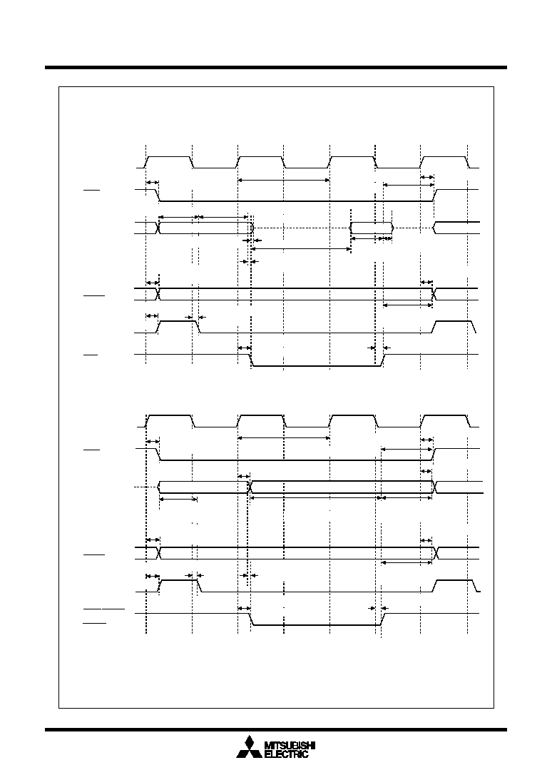
Mitsubishi microcomputers
M16C / 62A Group
SINGLE-CHIP 16-BIT CMOS MICROCOMPUTER
Timing (Vcc = 5V)
187
Memory Expansion Mode and Microprocessor Mode
(When accessing external memory area with wait, and select multiplexed bus)
BCLK
CSi
ALE
RD
4ns.min
tcyc
ADi
BHE
ADi
/DBi
t
d(AD≠ALE)
Read timing
0ns.min
BCLK
CSi
ALE
≠4ns.min
4ns.min
4ns.min
tcyc
ADi
BHE
ADi
/DBi
Write timing
Address
Measuring conditions :
∑ V
CC
=5V
∑ Input timing voltage : Determined with
V
IL
=0.8V, V
IH
=2.5V
∑ Output timing voltage : Determined with V
OL
=0.8V, V
OH
=2.0V
(tcyc/2)ns.min
Address
Data input
(tcyc/2)ns.min
t
d(BCLK≠ALE)
(tcyc/2)ns.min
t
h(WR≠CS)
Address
(tcyc*3/2≠40)ns.min
t
d(BCLK≠ALE)
(tcyc/2)ns.min
(tcyc/2-25)ns.min
Address
25ns.max
t
SU(DB≠RD)
tac3(RD≠DB)
(tcyc/2)ns.min
t
h(ALE≠AD)
30ns.min
t
d(AD≠RD)
0ns.min
t
dz(RD≠AD)
8ns.max
t
d(AD≠WR)
0ns.min
Data output
WR,WRL,
WRH
t
d(BCLK≠CS)
25ns.max
t
h(RD≠CS)
t
h(BCLK≠CS)
4ns.min
t
h(BCLK≠AD)
t
h(RD≠DB)
0ns.min
40ns.min
25ns.max
t
d(BCLK≠AD)
≠4ns.min
t
h(BCLK≠ALE)
t
d(BCLK≠RD)
25ns.max
t
h(RD≠AD)
t
h(BCLK≠RD)
0ns.min
t
d(BCLK≠CS)
25ns.max
t
h(BCLK≠CS)
t
h(BCLK≠DB)
4ns.min
t
h(WR≠DB)
t
d(DB≠WR)
t
h(BCLK≠AD)
t
d(AD≠ALE)
(tcyc/2≠25)ns.min
t
d(BCLK≠AD)
25ns.max
25ns.max
t
h(BCLK≠ALE)
25ns.max
t
d(BCLK≠WR)
t
h(BCLK≠WR)
t
h(WR≠AD)
t
d(BCLK≠DB)
40ns.max
V
CC
= 5V
Figure 1.23.6. V
CC
= 5V timing diagram (5)

Mitsubishi microcomputers
M16C / 62A Group
SINGLE-CHIP 16-BIT CMOS MICROCOMPUTER
Electrical characteristics (Vcc = 3V)
188
S
y
m
b
o
l
V
O
H
H
I
G
H
o
u
t
p
u
t
v
o
l
t
a
g
e
V
O
H
V
O
L
L
O
W
o
u
t
p
u
t
v
o
l
t
a
g
e
L
O
W
o
u
t
p
u
t
v
o
l
t
a
g
e
V
O
L
H
I
G
H
o
u
t
p
u
t
v
o
l
t
a
g
e
S
t
a
n
d
a
r
d
T
y
p
.
U
n
i
t
Measuring condition
V
V
X
O
U
T
2
.
5
2.5
V
0
.
5
V
X
OUT
0
.
5
0
.
5
M
i
n
M
a
x
.
2
.
5
P
a
r
a
m
e
t
e
r
I
O
H
=
-
1
m
A
I
O
H
=
-
0
.
1
m
A
I
OH
= -50µA
I
O
L
=
1
m
A
I
O
L
=
0
.
1
m
A
I
O
L
=
5
0
µ
A
P
0
0
t
o
P
0
7
,
P
1
0
t
o
P
1
7
,
P
2
0
t
o
P
2
7
,
P
0
0
t
o
P
0
7
,
P
1
0
t
o
P
1
7
,
P
2
0
t
o
P
2
7
,
P
3
0
t
o
P
3
7
,
P
4
0
t
o
P
4
7
,
P
5
0
t
o
P
5
7
,
P
3
0
t
o
P
3
7
,
P
4
0
t
o
P
4
7
,
P
5
0
t
o
P
5
7
,
P
6
0
t
o
P
6
7
,
P
7
2
t
o
P
7
7
,
P
8
0
t
o
P
8
4
,
H
I
G
H
P
O
W
E
R
LOWPOWER
P
8
6
,
P
8
7
,
P
9
0
t
o
P
9
7
,
P
1
0
0
t
o
P
1
0
7
H
I
G
H
P
O
W
E
R
L
O
W
P
O
W
E
R
P
6
0
t
o
P
6
7
,
P
7
0
t
o
P
7
7
,
P
8
0
t
o
P
8
4
,
P
8
6
,
P
8
7
,
P
9
0
t
o
P
9
7
,
P
1
0
0
t
o
P
1
0
7
H
I
G
H
P
O
W
E
R
L
O
W
P
O
W
E
R
H
I
G
H
o
u
t
p
u
t
v
o
l
t
a
g
e X
C
O
U
T
W
i
t
h
n
o
l
o
a
d
a
p
p
l
i
e
d
W
i
t
h
n
o
l
o
a
d
a
p
p
l
i
e
d
3
.
0
1
.
6
V
H
y
s
t
e
r
e
s
i
s
H
y
s
t
e
r
e
s
i
s
H
I
G
H
i
n
p
u
t
c
u
r
r
e
n
t
I
IH
L
O
W
i
n
p
u
t
c
u
r
r
e
n
t
I
I
L
V
RAM
RAM retention voltage
Icc
Power supply current
V
T+-
V
T-
V
T
+
-
V
T
-
0.2
0.8
V
0.2
1.8
V
P0
0
to P0
7
, P1
0
to P1
7
, P2
0
to P2
7
,
P3
0
to P3
7
, P4
0
to P4
7
,P5
0
to P5
7
,
P6
0
to P6
7
, P7
0
to P7
7
, P8
0
to P8
7
,
P9
0
to P9
7
, P10
0
to P10
7,
4.0
µA
µA
When clock is stopped
2
.
0
V
RESET
X
I
N
,
R
E
S
E
T
,
C
N
V
s
s
,
B
Y
T
E
V
I
= 3V
V
I
= 0V
-4.0
P0
0
to P0
7
, P1
0
to P1
7
, P2
0
to P2
7
,
P3
0
to P3
7
, P4
0
to P4
7
, P5
0
to P5
7
,
P6
0
to P6
7
, P7
0
to P7
7
, P8
0
to P8
7
,
P9
0
to P9
7
, P10
0
to P10
7,
X
I
N
,
R
E
S
E
T
,
C
N
V
s
s
,
B
Y
T
E
Square wave
f(X
CIN
) = 32kHz
40.0
µ
A
R
f
X
I
N
R
f
X
C
I
N
Feedback resistance
X
IN
Feedback resistance
X
CIN
1
0
.
0
3
.
0
M
M
Square wave, no division
f(X
IN
) = 10MHz
mA
8
.
5
2
1
.
2
5
Mask ROM
version
R
P
U
L
L
U
P
120.0
k
P
0
0
t
o
P
0
7
,
P
1
0
t
o
P
1
7
,
P
2
0
t
o
P
2
7
,
P
3
0
t
o
P
3
7
,
P
4
0
t
o
P
4
7
,
P
5
0
t
o
P
5
7
,
P
6
0
t
o
P
6
7
,
P
7
2
t
o
P
7
7
,
P
8
0
t
o
P
8
4
,
P
8
6
,
P
8
7
,
P
9
0
t
o
P
9
7
,
P
1
0
0
t
o
P
1
0
7
LOW output voltage
V
X
COUT
0
0
W
i
t
h
n
o
l
o
a
d
a
p
p
l
i
e
d
W
i
t
h
n
o
l
o
a
d
a
p
p
l
i
e
d
H
I
G
H
P
O
W
E
R
LOWPOWER
V
I
=
0
V
66.0
500.0
In single-chip
mode, the
output pins are
open and other
pins are V
SS
Pull-up
resistance
S
q
u
a
r
e
w
a
v
e
,
n
o
d
i
v
i
s
i
o
n
f(X
IN
) = 10MHz
mA
1
2
.
0
2
1
.
2
5
F
l
a
s
h
m
e
m
o
r
y
5
V
v
e
r
s
i
o
n
Ma
s
k
R
O
M
v
e
r
s
i
o
n
Square wave, in RAM
f(X
CIN
) = 32kHz
µA
Flash memory
5V version
CLK
0
to CLK
4
,TA2
OUT
to TA4
OUT
,
T
B
0
I
N
t
o
T
B
5
I
N
,
I
N
T
0
t
o
I
N
T
5
,
N
M
I
,
AD
TRG
, CTS
0
to CTS
2
, SCL, SDA
H
O
L
D
,
R
D
Y
,
T
A
0
I
N
t
o
T
A
4
I
N
,
K
I
0
t
o
K
I
3
,
R
x
D
0
t
o
R
x
D
2
,
S
I
N
3
,
S
I
N
4
1
.
0
µA
20.0
0
.
9
µ
A
2
.
8
µ
A
f(X
CIN
) = 32kHz
f(X
CIN
) = 32kHz
T
o
p
r
=
8
5
∞
C
w
h
e
n
c
l
o
c
k
i
s
s
t
o
p
p
e
d
T
o
p
r
=
2
5
∞
C
w
h
e
n
c
l
o
c
k
i
s
s
t
o
p
p
e
d
W
h
e
n
a
W
A
I
T
i
n
s
t
r
u
c
t
i
o
n
i
s
e
x
e
c
u
t
e
d
.
O
s
c
i
l
l
a
t
i
o
n
c
a
p
a
c
i
t
y
H
i
g
h
(
N
o
t
e
3
)
W
h
e
n
a
W
A
I
T
i
n
s
t
r
u
c
t
i
o
n
i
s
e
x
e
c
u
t
e
d
.
O
s
c
i
l
l
a
t
i
o
n
c
a
p
a
c
i
t
y
L
o
w
(
N
o
t
e
3
)
S
q
u
a
r
e
w
a
v
e
,
i
n
f
l
a
s
h
m
e
m
o
r
y
f(X
CIN
) = 32kHz
8
0
0
µ
A
F
l
a
s
h
m
e
m
o
r
y
5
V
v
e
r
s
i
o
n
40.0
N
o
t
e
1
:
S
p
e
c
i
f
y
a
p
r
o
d
u
c
t
o
f
-
4
0
∞
C
t
o
8
5
∞
C
t
o
u
s
e
i
t
.
N
o
t
e
2
:
1
0
M
H
z
f
o
r
t
h
e
m
a
s
k
R
O
M
v
e
r
s
i
o
n
a
n
d
f
l
a
s
h
m
e
m
o
r
y
5
V
v
e
r
s
i
o
n
.
N
o
t
e
3
:
W
i
t
h
o
n
e
t
i
m
e
r
o
p
e
r
a
t
e
d
u
s
i
n
g
f
C
3
2
.
10
10
(Topr
= 25
∞
C)
(Topr
= 25
∞
C)
V
CC
= 3V
Table 1.23.23. Electrical characteristics (referenced to V
CC
= 2.7 to 3.3V, V
SS
= 0V at Topr = ≠ 20
o
C
to 85
o
C / ≠ 40
o
C to 85
o
C (Note 1), f(X
IN
) = 10MH
Z
(Note 2) with wait unless otherwise
specified)

Mitsubishi microcomputers
M16C / 62A Group
SINGLE-CHIP 16-BIT CMOS MICROCOMPUTER
Timing (Vcc = 3V)
189
9
10
Min.
Data input setup time
ns
t
su(DB-RD)
t
su(RDY-BCLK )
Parameter
Symbol
Unit
Max.
Standard
RDY input setup time
ns
Data input hold time
ns
t
h(RD-DB)
t
h(BCLK -RDY)
ns
RDY input hold time
ns
HOLD input setup time
t
su(HOLD-BCLK )
ns
HOLD input hold time
t
h(BCLK-HOLD )
Data input access time (no wait)
ns
t
ac1(RD-DB)
ns
ns
t
ac2(RD-DB)
t
ac3(RD-DB)
Data input access time (with wait)
Data input access time (when accessing multiplex bus area)
ns
HLDA output delay time
t
d(BCLK-HLDA)
80
60
0
0
80
0
(Note)
(Note)
(Note)
Note: Calculated according to the BCLK frequency as follows:
100
ns
ns
t
c
t
w(H
)
t
w(L)
t
r
t
f
Max.
Min.
Parameter
Symbol
Unit
Standard
External clock rise time
External clock input
cycle time
External clock input
HIGH pulse width
External clock input
LOW pulse width
External clock fall time
18
18
t
ac1(RD ≠ DB) =
f(BCLK) X 2
≠ 90
[ns]
t
ac2(RD ≠ DB) =
f(BCLK) X 2
≠ 90
3 X 10
9
[ns]
t
ac3(RD ≠ DB) =
f(BCLK) X 2
≠ 90
3 X 10
9
[ns]
Mask ROM, Flash memory 5V version
Mask ROM, Flash memory 5V version
Mask ROM, Flash memory 5V version
ns
100
ns
40
ns
40
V
CC
= 3V
Table 1.23.25. Memory expansion and microprocessor modes
Timing requirements (referenced to V
CC
= 3V, V
SS
= 0V at Topr = ≠ 20
o
C to 85
o
C / ≠ 40
o
C to 85
o
C (*)
unless otherwise specified)
* : Specify a product of -40
∞
C to 85
∞
C to use it.
Table 1.23.24. External clock input

Mitsubishi microcomputers
M16C / 62A Group
SINGLE-CHIP 16-BIT CMOS MICROCOMPUTER
Timing (Vcc = 3V)
190
V
CC
= 3V
Timing requirements (referenced to V
CC
= 3V, V
SS
= 0V at Topr = ≠ 20
o
C to 85
o
C / ≠ 40
o
C to 85
o
C (*)
unless otherwise specified)
* : Specify a product of -40
∞
C to 85
∞
C to use it.
Standard
Max.
Min.
Unit
Parameter
Symbol
ns
t
w(TAL)
TAi
IN
input LOW pulse width
60
ns
t
c(TA)
TAi
IN
input cycle time
150
ns
t
w(TAH)
TAi
IN
input HIGH pulse width
60
Standard
Max.
Min.
Unit
Parameter
Symbol
ns
t
c(TA)
TAi
IN
input cycle time
600
ns
t
w(TAH)
TAi
IN
input HIGH pulse width
300
ns
t
w(TAL)
TAi
IN
input LOW pulse width
300
Standard
Max.
Min.
Unit
Parameter
Symbol
ns
t
c(TA)
TAi
IN
input cycle time
300
ns
t
w(TAH)
TAi
IN
input HIGH pulse width
150
ns
t
w(TAL)
TAi
IN
input LOW pulse width
150
Standard
Max.
Min.
Unit
Parameter
Symbol
ns
t
w(TAH)
TAi
IN
input HIGH pulse width
150
ns
t
w(TAL)
TAi
IN
input LOW pulse width
150
Standard
Max.
Min.
Unit
Parameter
Symbol
ns
t
c(UP)
TAi
OUT
input cycle time
3000
ns
t
w(UPH)
TAi
OUT
input HIGH pulse width
1500
ns
t
w(UPL)
TAi
OUT
input LOW pulse width
1500
ns
t
su(UP-T
IN
)
TAi
OUT
input setup time
600
ns
t
h(T
IN-
UP)
TAi
OUT
input hold time
600
Table 1.23.27. Timer A input (gating input in timer mode)
Table 1.23.28. Timer A input (external trigger input in one-shot timer mode)
Table 1.23.29. Timer A input (external trigger input in pulse width modulation mode)
Table 1.23.30. Timer A input (up/down input in event counter mode)
Table 1.23.26. Timer A input (counter input in event counter mode)

Mitsubishi microcomputers
M16C / 62A Group
SINGLE-CHIP 16-BIT CMOS MICROCOMPUTER
Timing (Vcc = 3V)
191
Timing requirements (referenced to V
CC
= 3V, V
SS
= 0V at Topr = ≠ 20
o
C to 85
o
C / ≠ 40
o
C to 85
o
C (*)
unless otherwise specified)
* : Specify a product of -40
∞
C to 85
∞
C to use it.
V
CC
= 3V
Standard
Max.
Min.
Parameter
Symbol
Unit
ns
t
c(TB)
TBi
IN
input cycle time (counted on one edge)
150
ns
t
w(TBH)
TBi
IN
input HIGH pulse width (counted on one edge)
60
ns
t
w(TBL)
TBi
IN
input LOW pulse width (counted on one edge)
60
t
w(TBH)
ns
TBi
IN
input HIGH pulse width (counted on both edges)
160
t
w(TBL)
ns
TBi
IN
input LOW pulse width (counted on both edges)
160
t
c(TB)
ns
TBi
IN
input cycle time (counted on both edges)
300
Standard
Max.
Min.
Parameter
Symbol
Unit
ns
t
c(TB)
TBi
IN
input cycle time
600
ns
t
w(TBH)
TBi
IN
input HIGH pulse width
300
t
w(TBL)
ns
TBi
IN
input LOW pulse width
300
Standard
Max.
Min.
Parameter
Symbol
Unit
ns
t
c(TB)
TBi
IN
input cycle time
600
ns
t
w(TBH)
TBi
IN
input HIGH pulse width
300
t
w(TBL)
ns
TBi
IN
input LOW pulse width
300
Standard
Max.
Min.
Parameter
Symbol
Unit
ns
t
c(AD)
AD
TRG
input cycle time (trigger able minimum)
1500
ns
t
w(ADL)
AD
TRG
input LOW pulse width
200
Standard
Max.
Min.
Parameter
Symbol
Unit
ns
t
w(INH)
INTi input HIGH pulse width
380
ns
t
w(INL)
INTi input LOW pulse width
380
Standard
Max.
Min.
Parameter
Symbol
Unit
ns
t
c(CK)
CLKi input cycle time
300
ns
t
w(CKH)
CLKi input HIGH pulse width
150
ns
t
w(CKL)
CLKi input LOW pulse width
150
t
h(C-Q)
ns
TxDi hold time
0
t
su(D-C)
ns
RxDi input setup time
50
t
h(C-D)
ns
RxDi input hold time
90
t
d(C-Q)
ns
TxDi output delay time
160
Table 1.23.31. Timer B input (counter input in event counter mode)
Table 1.23.32. Timer B input (pulse period measurement mode)
Table 1.23.33. Timer B input (pulse width measurement mode)
Table 1.23.34. A-D trigger input
Table 1.23.35. Serial I/O
_______
Table 1.23.36. External interrupt INTi inputs
Mitsubishi microcomputers
M16C / 62A Group
SINGLE-CHIP 16-BIT CMOS MICROCOMPUTER
Timing (Vcc = 3V)
192
t
d(BCLK-AD)
Address output delay time
60
ns
t
d(BCLK-CS)
Chip select output delay time
60
ns
t
h(BCLK-AD)
Address output hold time (BCLK standard)
4
ns
t
h(BCLK-CS)
Chip select output hold time (BCLK standard)
4
ns
t
d(BCLK-ALE)
ALE signal output delay time
60
ns
t
h(BCLK-ALE)
ALE signal output hold time
--
4
ns
t
d(BCLK-RD)
RD signal output delay time
60
ns
t
h(BCLK-RD)
RD signal output hold time
0
ns
t
h(RD-AD)
Address output hold time (RD standard)
0
ns
t
d(BCLK-WR)
WR signal output delay time
60
ns
t
h(BCLK-WR)
WR signal output hold time
0
ns
t
h(WR-AD)
Address output hold time (WR standard)
0
ns
t
d(BCLK-DB)
Data output delay time (BCLK standard)
80
ns
t
h(BCLK-DB)
Data output hold time (BCLK standard)
4
ns
t
d(DB-WR)
Data output delay time (WR standard)
(Note1)
ns
t
h(WR-DB)
Data output hold time (WR standard)(Note2)
0
ns
Note 1: Calculated according to the BCLK frequency as follows:
td(DB ≠ WR) =
f(BCLK) X 2
10
9
≠ 80
[ns]
Symbol
Standard
Measuring condition
Max.
Min.
Parameter
Unit
Note 2: This is standard value shows the timing when the output is off,
and doesn't show hold time of data bus.
Hold time of data bus is different by capacitor volume and pull-up
(pull-down) resistance value.
Hold time of data bus is expressed in
t = ≠CR X ln (1 ≠ V
OL
/ V
CC
)
by a circuit of the right figure.
For example, when V
OL
= 0.2V
CC
, C = 30pF, R = 1k
, hold time
of output "L" level is
t = ≠ 30pF X 1k
X ln (1 ≠ 0.2V
CC
/ V
CC
)
= 6.7ns.
DBi
R
C
Note 3: Specify a product of -40∞C to 85∞C to use it.
Switching characteristics (referenced to V
CC
= 3V, V
SS
= 0V at Topr = ≠ 20
o
C to 85
o
C / ≠ 40
o
C to
85
o
C (Note 3), CM15="1" unless otherwise specified)
V
CC
= 3V
Figure 1.23.7
Table 1.23.37. Memory expansion and microprocessor modes (with no wait)
Figure 1.23.7. Port P0 to P10 measurement circuit
P6
P7
P8
P10
P9
P0
P1
P2
P3
P4
P5
30pF
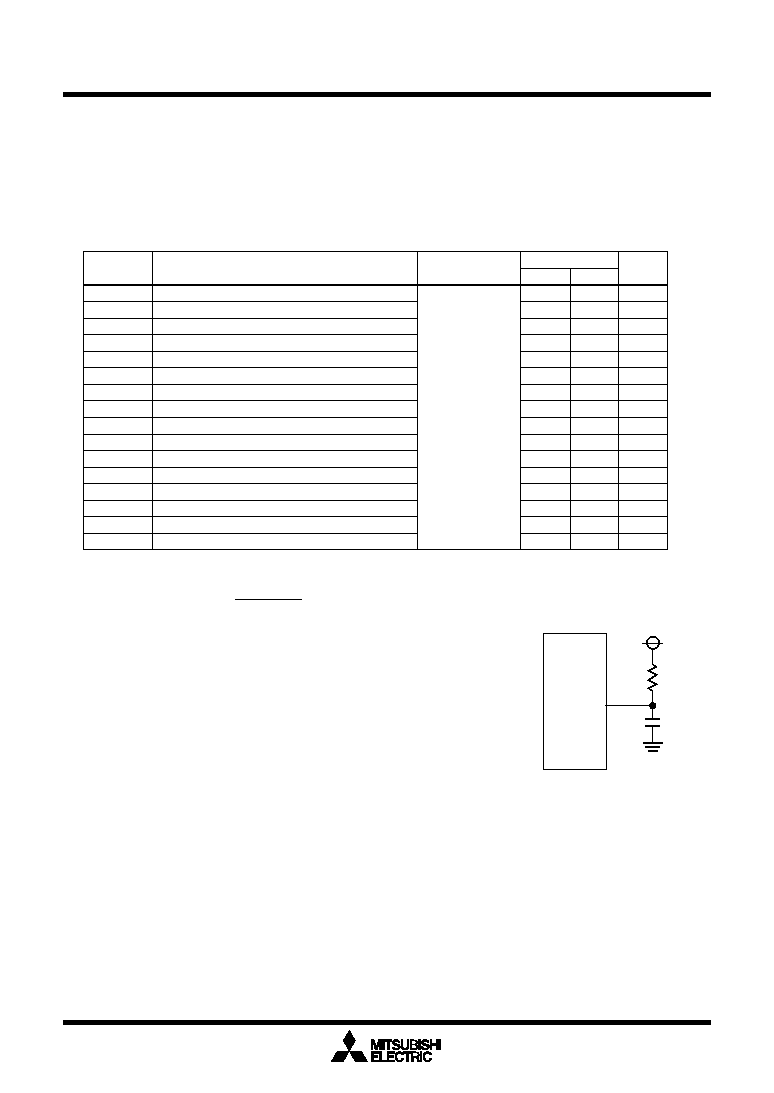
Mitsubishi microcomputers
M16C / 62A Group
SINGLE-CHIP 16-BIT CMOS MICROCOMPUTER
Timing (Vcc = 3V)
193
Switching characteristics (referenced to V
CC
= 3V, V
SS
= 0V at Topr = ≠ 20
o
C to 85
o
C / ≠ 40
o
C to
85
o
C (Note 3), CM15="1" unless otherwise specified)
V
CC
= 3V
Figure 1.23.7
Table 1.23.38. Memory expansion and microprocessor modes
(when accessing external memory area with wait)
t
d(BCLK-AD)
Address output delay time
60
ns
t
d(BCLK-CS)
Chip select output delay time
60
ns
t
h(BCLK-AD)
Address output hold time (BCLK standard)
4
ns
t
h(BCLK-CS)
Chip select output hold time (BCLK standard)
4
ns
t
d(BCLK-ALE)
ALE signal output delay time
60
ns
t
h(BCLK-ALE)
ALE signal output hold time
≠ 4
ns
t
d(BCLK-RD)
RD signal output delay time
60
ns
t
h(BCLK-RD)
RD signal output hold time
0
ns
t
h(RD-AD)
Address output hold time (RD standard)
0
ns
t
d(BCLK-WR)
WR signal output delay time
60
ns
t
h(BCLK-WR)
WR signal output hold time
0
ns
t
h(WR-AD)
Address output hold time (WR standard)
0
ns
t
d(BCLK-DB)
Data output delay time (BCLK standard)
80
ns
t
h(BCLK-DB)
Data output hold time (BCLK standard)
4
ns
t
d(DB-WR)
Data output delay time (WR standard)
(Note1)
ns
t
h(WR-DB)
Data output hold time (WR standard)(Note2)
0
ns
Note 1: Calculated according to the BCLK frequency as follows:
td(DB ≠ WR) =
f(BCLK)
10
9
≠ 80
[ns]
Symbol
Standard
Measuring condition
Max.
Min.
Parameter
Unit
Note 2: This is standard value shows the timing when the output is off,
and doesn't show hold time of data bus.
Hold time of data bus is different by capacitor volume and pull-up
(pull-down) resistance value.
Hold time of data bus is expressed in
t = ≠CR X ln (1 ≠ V
OL
/ V
CC
)
by a circuit of the right figure.
For example, when V
OL
= 0.2V
CC
, C = 30pF, R = 1k
, hold time
of output "L" level is
t = ≠ 30pF X 1k
X ln (1 ≠ 0.2V
CC
/ V
CC
)
= 6.7ns.
DBi
R
C
Note 3: Specify a product of -40∞C to 85∞C to use it.

Mitsubishi microcomputers
M16C / 62A Group
SINGLE-CHIP 16-BIT CMOS MICROCOMPUTER
Timing (Vcc = 3V)
194
V
CC
= 3V
Switching characteristics (referenced to V
CC
= 3V, V
SS
= 0V at Topr = ≠ 20
o
C to 85
o
C / ≠ 40
o
C to
85
o
C (Note 2), CM15="1" unless otherwise specified)
Table 1.23.39. Memory expansion and microprocessor modes
(when accessing external memory area with wait, and select multiplexed bus)
Symbol
Standard
Measuring condition
Max.
Min.
Parameter
Unit
t
d(BCLK-AD)
Address output delay time
60
ns
t
h(BCLK-AD)
Address output hold time (BCLK standard)
4
ns
t
d(BCLK-CS)
Chip select output delay time
60
ns
t
h(BCLK-CS)
Chip select output hold time (BCLK standard)
4
ns
ns
t
h(RD-AD)
Address output hold time (RD standard)
(Note1)
t
d(BCLK-RD)
RD signal output delay time
60
ns
t
h(BCLK-RD)
RD signal output hold time
0
ns
ns
t
h(WR-AD)
Address output hold time (WR standard)
(Note1)
t
d(BCLK-WR)
WR signal output delay time
60
ns
t
d(BCLK-DB)
Data output delay time (BCLK standard)
80
ns
t
h(BCLK-DB)
Data output hold time (BCLK standard)
4
ns
t
d(DB-WR)
Data output delay time (WR standard)
(Note1)
ns
t
h(BCLK-ALE)
ALE signal output hold time (BCLK standard)
≠ 4
ns
t
d(AD-ALE)
ALE signal output delay time (Address standard)
(Note1)
ns
t
h(ALE-AD)
ALE signal output hold time(Address standard)
50
ns
t
h(BCLK-WR)
WR signal output hold time
0
ns
ns
t
h(RD-CS)
Chip select output hold time (RD standard)
(Note1)
t
h(WR-CS)
Chip select output hold time (WR standard)
(Note1)
ns
t
d(AD-RD)
Post-address RD signal output delay time
ns
0
t
d(AD-WR)
Post-address WR signal output delay time
ns
0
t
dZ(RD-AD)
Address output floating start time
ns
8
t
d(BCLK-ALE)
ALE signal output delay time (BCLK standard)
ns
60
Note: Calculated according to the BCLK frequency as follows:
th(RD ≠ AD) =
f(BCLK) X 2
10
9
[ns]
th(WR ≠ AD) =
f(BCLK) X 2
10
9
[ns]
th(RD ≠ CS) =
f(BCLK) X 2
10
9
[ns]
th(WR ≠ CS) =
f(BCLK) X 2
10
9
[ns]
td(DB ≠ WR) =
f(BCLK) X 2
10
9
≠ 80
[ns]
X 3
td(AD ≠ ALE) =
f(BCLK) X 2
10
9
≠ 45
[ns]
th(WR ≠ DB) =
f(BCLK) X 2
10
9
[ns]
t
h(WR-DB)
Data output hold time (WR standard)
ns
(Note1)
Note 2: Specify a product of -40∞C to 85∞C to use it.
Figure 1.23.7

Mitsubishi microcomputers
M16C / 62A Group
SINGLE-CHIP 16-BIT CMOS MICROCOMPUTER
Timing (Vcc = 3V)
195
V
CC
= 3V
t
su(D≠C)
TAi
IN
input
TAi
OUT
input
During event counter mode
TBi
IN
input
CLKi
TxDi
RxDi
t
c(TA)
t
w(TAH)
t
w(TAL)
t
c(UP)
t
w(UPH)
t
w(UPL)
t
c(TB)
t
w(TBH)
t
w(TBL)
t
c(AD)
t
w(ADL)
t
c(CK)
t
w(CKH)
t
w(CKL)
t
w(INL)
t
w(INH)
t
d(C≠Q)
t
h(C≠D)
t
h(C≠Q)
t
h(T
IN
≠UP)
t
su(UP≠T
IN
)
TAi
IN
input
(When count on falling
edge is selected)
TAi
IN
input
(When count on rising
edge is selected)
TAi
OUT
input
(Up/down input)
INTi input
AD
TRG
input
Figure 1.23.8. V
CC
= 3V timing diagram (1)

Mitsubishi microcomputers
M16C / 62A Group
SINGLE-CHIP 16-BIT CMOS MICROCOMPUTER
Timing (Vcc = 3V)
196
V
CC
= 3V
Measuring conditions :
∑ V
CC
=3V
∑ Input timing voltage : Determined with V
IL
=0.6V, V
IH
=2.4V
∑ Output timing voltage : Determined with V
OL
=1.5V, V
OH
=1.5V
Memory Expansion Mode and Microprocessor Mode
BCLK
HOLD input
HLDA output
P0, P1, P2,
P3, P4,
P5
0
to P5
2
(Valid with or without wait)
Note: The above pins are set to high-impedance regardless of the input level of the
BYTE pin and bit (PM06) of processor mode register 0 selects the function of
ports
P4
0
to P4
3
.
t
h(BCLK≠HOLD)
t
su(HOLD≠BCLK)
(Valid only with wait)
t
d(BCLK≠HLDA)
t
d(BCLK≠HLDA)
Hi≠Z
RDY input
tsu(RDY≠BCLK)
th(BCLK≠RDY)
BCLK
RD
(Multiplexed bus)
(Multiplexed bus)
WR, WRL, WRH
WR, WRL, WRH
(Separate bus)
RD
(Separate bus)
Figure 1.23.9. V
CC
= 3V timing diagram (2)

Mitsubishi microcomputers
M16C / 62A Group
SINGLE-CHIP 16-BIT CMOS MICROCOMPUTER
Timing (Vcc = 3V)
197
Read timing
Write timing
BCLK
CSi
ALE
RD
60ns.max
4ns.min
4ns.min
Hi≠Z
DB
0ns.min
ADi
BHE
tcyc
80ns.min
BCLK
CSi
ALE
≠4ns.min
60ns.max
0ns.min
4ns.min
Hi≠Z
DB
4ns.min
ADi
BHE
tcyc
t
h(BCLK≠ALE)
t
h(BCLK≠DB)
t
d(BCLK≠ALE)
t
d(BCLK≠WR)
0ns.min
t
h(WR≠AD)
Memory Expansion Mode and Microprocessor Mode
(With no wait)
WR,WRL,
WRH
t
d(BCLK≠CS)
60ns.max
t
h(BCLK≠CS)
t
h(RD≠CS)
t
d(BCLK≠AD)
60ns.max
t
h(BCLK≠AD)
60ns.max
t
d(BCLK≠ALE)
≠4ns.min
t
h(RD≠AD) 0ns.min
t
d(BCLK≠RD)
t
h(BCLK≠RD)
t
ac1(RD≠DB)
t
h(RD≠DB)
0ns.min
t
SU(DB≠RD)
t
d(BCLK≠CS)
t
h(BCLK≠CS)
4ns.min
60ns.max
0ns.min
t
h(WR≠CS)
t
d(BCLK≠AD)
60ns.max
t
h(BCLK≠AD)
60ns.max
t
h(BCLK≠ALE)
t
h(BCLK≠WR)
t
d(BCLK≠DB)
t
h(WR≠DB)
t
d(DB≠WR)
(tcyc/2≠80)ns.min
0ns.min
80ns.max
0ns.min
V
CC
= 3V
Figure 1.23.10. V
CC
= 3V timing diagram (3)
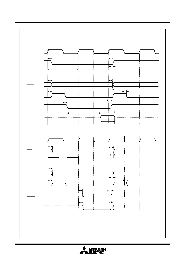
Mitsubishi microcomputers
M16C / 62A Group
SINGLE-CHIP 16-BIT CMOS MICROCOMPUTER
Timing (Vcc = 3V)
198
Read timing
Write timing
BCLK
CSi
ALE
RD
4ns.min
4ns.min
Hi≠Z
DB
80ns.min
0ns.min
ADi
BHE
t
d(BCLK≠WR)
60ns.max
t
h(BCLK≠WR)
0ns.min
BCLK
CSi
t
d(BCLK≠CS)
60ns.max
t
d(BCLK≠AD)
ALE
t
h(BCLK≠ALE)
t
h(BCLK≠CS)
4ns.min
tcyc
0ns.min
t
h(WR≠CS)
0ns.min
t
h(WR≠AD)
ADi
BHE
t
d(BCLK≠DB)
4ns.min
t
h(BCLK≠DB)
t
d(DB≠WR)
(tcyc≠80)ns.min
0ns.min
t
h(WR≠DB)
DBi
t
h(RD≠AD)
0ns.min
t
d(BCLK≠ALE)
60ns.max
t
SU(DB≠RD)
Memory Expansion Mode and Microprocessor Mode
(When accessing external memory area with wait)
Measuring conditions :
∑ V
CC
=3V
∑ Input timing voltage : Determined with V
IL
=0.48V, V
IH
=1.5V
∑ Output timing voltage : Determined with V
OL
=1.5V, V
OH
=1.5V
WR,WRL,
WRH
t
d(BCLK≠CS)
60ns.max
t
h(RD≠CS)
tcyc
t
d(BCLK≠AD)
60ns.max
t
h(BCLK≠AD)
≠4ns.min
t
h(BCLK≠ALE)
60ns.max
t
d(BCLK≠RD)
t
h(BCLK≠RD) 0ns.min
t
ac2(RD≠DB)
t
h(RD≠DB) 0ns.min
t
h(BCLK≠AD)
60ns.max
t
d(BCLK≠ALE) 60ns.max
≠4ns.min
80ns.max
t
h(BCLK≠CS)
4ns.min
V
CC
= 3V
Figure 1.23.11. V
CC
= 3V timing diagram (4)

Mitsubishi microcomputers
M16C / 62A Group
SINGLE-CHIP 16-BIT CMOS MICROCOMPUTER
Timing (Vcc = 3V)
199
Memory Expansion Mode and Microprocessor Mode
(When accessing external memory area with wait, and select multiplexed bus)
Measuring conditions :
∑ V
CC
=3V
∑ Input timing voltage : Determined with V
IL
=0.48V,V
IH
=1.5V
∑ Output timing voltage : Determined with V
OL
=1.5V,V
OH
=1.5V
Read timing
Write timing
0ns.min
BCLK
CSi
ALE
60ns.max
≠4ns.min
t
h(BCLK≠CS)
4ns.min
tcyc
ADi
BHE
80ns.max
t
h(BCLK≠DB)
4ns.min
t
d(DB≠WR)
(tcyc*3/2≠80)ns.min
ADi
/DBi
Address
Data output
(tcyc/2)ns.min
Address
(tcyc/2≠60)ns.min
t
d(BCLK≠ALE)
t
d(BCLK≠WR)
4ns.min
BCLK
CSi
t
d(BCLK≠CS)
60ns.max
ALE
RD
4ns.min
t
h(BCLK≠CS)
4ns.min
tcyc
ADi
BHE
ADi
/DBi
t
h(RD≠DB)
0ns.min
Address
(tcyc/2)ns.min
Data input
Address
tac3(RD≠DB)
t
dz(RD≠AD)
8ns.max
t
d(AD≠RD)
0ns.min
t
d(AD≠WR)
WR,WRL,
WRH
t
h(RD≠CS)
t
d(AD≠ALE) (tcyc/2≠45)ns.min
t
SU(DB≠RD)
80ns.min
t
h(ALE≠AD)
50ns.min
t
d(BCLK≠AD)
60ns.max
60ns.max
t
d(BCLK≠ALE)
t
h(BCLK≠ALE)
≠4ns.min
(tcyc/2)ns.min
t
h(RD≠AD)
t
h(BCLK≠AD)
t
h(BCLK≠RD)
0ns.min
t
d(BCLK≠RD)
60ns.max
t
d(BCLK≠CS)
60ns.max
t
h(WR≠CS)
(tcyc/2)ns.min
t
d(BCLK≠DB)
t
d(AD≠ALE)
t
d(BCLK≠AD)
60ns.max
t
h(WR≠DB)
(tcyc/2)ns.min
t
h(BCLK≠AD)
t
h(WR≠AD)
t
h(BCLK≠WR)
t
h(BCLK≠ALE)
0ns.min
60ns.max
V
CC
= 3V
Figure 1.23.12. V
CC
= 3V timing diagram (5)

Mitsubishi microcomputers
M16C / 62A Group
SINGLE-CHIP 16-BIT CMOS MICROCOMPUTER
GZZ-SH13-36B<96A0>
MITSUBISHI ELECTRIC-CHIP 16-BIT
MICROCOMPUTER M30620M8A-XXXFP/GP
MASK ROM CONFIRMATION FORM
Mask ROM number
200
Date :
TEL
( )
Receipt
Section head
signature
Supervisor
signature
Customer
Company
name
Date
issued
Date :
Note : Please complete all items marked
.
Issuance
signature
Submitted by
Supervisor
1. Check sheet
Mitsubishi processes the mask files generated by the mask file generation utilities out of those held on
the floppy disks you give in to us, and forms them into masks. Hence, we assume liability provided that
there is any discrepancy between the contents of these mask files and the ROM data to be burned into
products we produce. Check thoroughly the contents of the mask files you give in.
Prepare 3.5 inches 2HD (IBM format) floppy disks. And store only one mask file in a floppy disk.
2. Mark specification
The mark specification differs according to the type of package. After entering the mark specification on
the separate mark specification sheet (for each package), attach that sheet to this masking check sheet
for submission to Mitsubishi.
For the M30620M8A-XXXFP, submit the 100P6S mark specification sheet. For the M30620M8A-XXXGP,
submit the 100P6Q mark specification sheet.
3. Usage Conditions
For our reference when of testing our products, please reply to the following questions about the usage
of the products you ordered.
(1) Which kind of X
IN
-X
OUT
oscillation circuit is used?
Ceramic resonator
Quartz-crystal oscillator
External clock input
Other ( )
What frequency do not use?
f(X
IN
) =
MH
Z
Microcomputer type No. :
M30620M8A-XXXFP
M30620M8A-XXXGP
File code :
(hex)
Mask file name :
.MSK (alpha-numeric 8-digit)

Mitsubishi microcomputers
M16C / 62A Group
SINGLE-CHIP 16-BIT CMOS MICROCOMPUTER
Mask ROM number
MITSUBISHI ELECTRIC-CHIP 16-BIT
MICROCOMPUTER M30620M8A-XXXFP/GP
MASK ROM CONFIRMATION FORM
GZZ-SH13-36B<96A0>
201
(2) Which kind of X
CIN
-X
COUT
oscillation circuit is used?
Ceramic resonator
Quartz-crystal oscillator
External clock input
Other ( )
What frequency do not use?
f(X
CIN
) =
kH
Z
(3) Which operation mode do you use?
Single-chip mode
Memory expansion mode
Microprocessor mode
(4) Which operating supply voltage do you use?
(Circle the operating voltage range of use)
2.4
2.7
3.0
3.3
3.5
3.8
4.0
4.2
4.5
4.7
5.0
5.3
5.5
5.7
(5) Which operating ambient temperature do you use?
(Circle the operating temperature range of use)
-50
-40
-30
-20
-10
0
10
20
30
40
50
60
70
80
90
(V)
(
∞
C)
(6) Do you use I
2
C (Inter IC) bus function?
Not use
Use
(7) Do you use IE (Inter Equipment) bus function?
Not use
Use
Thank you cooperation.
4. Special item (Indicate none if there is not specified item)

Mitsubishi microcomputers
M16C / 62A Group
SINGLE-CHIP 16-BIT CMOS MICROCOMPUTER
GZZ-SH13-37B<96A0>
MITSUBISHI ELECTRIC-CHIP 16-BIT
MICROCOMPUTER M30620MAA-XXXFP/GP
MASK ROM CONFIRMATION FORM
Mask ROM number
202
Date :
TEL
( )
Receipt
Section head
signature
Supervisor
signature
Customer
Company
name
Date
issued
Date :
Note : Please complete all items marked
.
Issuance
signature
Submitted by
Supervisor
1. Check sheet
Mitsubishi processes the mask files generated by the mask file generation utilities out of those held on
the floppy disks you give in to us, and forms them into masks. Hence, we assume liability provided that
there is any discrepancy between the contents of these mask files and the ROM data to be burned into
products we produce. Check thoroughly the contents of the mask files you give in.
Prepare 3.5 inches 2HD (IBM format) floppy disks. And store only one mask file in a floppy disk.
2. Mark specification
The mark specification differs according to the type of package. After entering the mark specification on
the separate mark specification sheet (for each package), attach that sheet to this masking check sheet
for submission to Mitsubishi.
For the M30620MAA-XXXFP, submit the 100P6S mark specification sheet. For the M30620MAA-XXXGP,
submit the 100P6Q mark specification sheet.
3. Usage Conditions
For our reference when of testing our products, please reply to the following questions about the usage
of the products you ordered.
(1) Which kind of X
IN
-X
OUT
oscillation circuit is used?
Ceramic resonator
Quartz-crystal oscillator
External clock input
Other ( )
What frequency do not use?
f(X
IN
) =
MH
Z
Microcomputer type No. :
M30620MAA-XXXFP
M30620MAA-XXXGP
File code :
(hex)
Mask file name :
.MSK (alpha-numeric 8-digit)

Mitsubishi microcomputers
M16C / 62A Group
SINGLE-CHIP 16-BIT CMOS MICROCOMPUTER
Mask ROM number
MITSUBISHI ELECTRIC-CHIP 16-BIT
MICROCOMPUTER M30620MAA-XXXFP/GP
MASK ROM CONFIRMATION FORM
GZZ-SH13-37B<96A0>
203
(2) Which kind of X
CIN
-X
COUT
oscillation circuit is used?
Ceramic resonator
Quartz-crystal oscillator
External clock input
Other ( )
What frequency do not use?
f(X
CIN
) =
kH
Z
(3) Which operation mode do you use?
Single-chip mode
Memory expansion mode
Microprocessor mode
(4) Which operating supply voltage do you use?
(Circle the operating voltage range of use)
2.4
2.7
3.0
3.3
3.5
3.8
4.0
4.2
4.5
4.7
5.0
5.3
5.5
5.7
(5) Which operating ambient temperature do you use?
(Circle the operating temperature range of use)
-50
-40
-30
-20
-10
0
10
20
30
40
50
60
70
80
90
(V)
(
∞
C)
(6) Do you use I
2
C (Inter IC) bus function?
Not use
Use
(7) Do you use IE (Inter Equipment) bus function?
Not use
Use
Thank you cooperation.
4. Special item (Indicate none if there is not specified item)

Mitsubishi microcomputers
M16C / 62A Group
SINGLE-CHIP 16-BIT CMOS MICROCOMPUTER
GZZ-SH13-28B<95A0>
MITSUBISHI ELECTRIC-CHIP 16-BIT
MICROCOMPUTER M30620MCA-XXXFP/GP
MASK ROM CONFIRMATION FORM
Mask ROM number
204
Date :
TEL
( )
Receipt
Section head
signature
Supervisor
signature
Customer
Company
name
Date
issued
Date :
Note : Please complete all items marked
.
Issuance
signature
Submitted by
Supervisor
1. Check sheet
Mitsubishi processes the mask files generated by the mask file generation utilities out of those held on
the floppy disks you give in to us, and forms them into masks. Hence, we assume liability provided that
there is any discrepancy between the contents of these mask files and the ROM data to be burned into
products we produce. Check thoroughly the contents of the mask files you give in.
Prepare 3.5 inches 2HD (IBM format) floppy disks. And store only one mask file in a floppy disk.
2. Mark specification
The mark specification differs according to the type of package. After entering the mark specification on
the separate mark specification sheet (for each package), attach that sheet to this masking check sheet
for submission to Mitsubishi.
For the M30620MCA-XXXFP, submit the 100P6S mark specification sheet. For the M30620MCA-XXXGP,
submit the 100P6Q mark specification sheet.
3. Usage Conditions
For our reference when of testing our products, please reply to the following questions about the usage
of the products you ordered.
(1) Which kind of X
IN
-X
OUT
oscillation circuit is used?
Ceramic resonator
Quartz-crystal oscillator
External clock input
Other ( )
What frequency do not use?
f(X
IN
) =
MH
Z
Microcomputer type No. :
M30620MCA-XXXFP
M30620MCA-XXXGP
File code :
(hex)
Mask file name :
.MSK (alpha-numeric 8-digit)

Mitsubishi microcomputers
M16C / 62A Group
SINGLE-CHIP 16-BIT CMOS MICROCOMPUTER
Mask ROM number
MITSUBISHI ELECTRIC-CHIP 16-BIT
MICROCOMPUTER M30620MCA-XXXFP/GP
MASK ROM CONFIRMATION FORM
GZZ-SH13-28B<95A0>
205
(2) Which kind of X
CIN
-X
COUT
oscillation circuit is used?
Ceramic resonator
Quartz-crystal oscillator
External clock input
Other ( )
What frequency do not use?
f(X
CIN
) =
kH
Z
(3) Which operation mode do you use?
Single-chip mode
Memory expansion mode
Microprocessor mode
(4) Which operating supply voltage do you use?
(Circle the operating voltage range of use)
2.4
2.7
3.0
3.3
3.5
3.8
4.0
4.2
4.5
4.7
5.0
5.3
5.5
5.7
(5) Which operating ambient temperature do you use?
(Circle the operating temperature range of use)
-50
-40
-30
-20
-10
0
10
20
30
40
50
60
70
80
90
(V)
(
∞
C)
(6) Do you use I
2
C (Inter IC) bus function?
Not use
Use
(7) Do you use IE (Inter Equipment) bus function?
Not use
Use
Thank you cooperation.
4. Special item (Indicate none if there is not specified item)

Mitsubishi microcomputers
M16C / 62A Group
SINGLE-CHIP 16-BIT CMOS MICROCOMPUTER
GZZ-SH13-40B<96A0>
MITSUBISHI ELECTRIC-CHIP 16-BIT
MICROCOMPUTER M30622M4A-XXXFP/GP
MASK ROM CONFIRMATION FORM
Mask ROM number
206
Date :
TEL
( )
Receipt
Section head
signature
Supervisor
signature
Customer
Company
name
Date
issued
Date :
Note : Please complete all items marked
.
Issuance
signature
Submitted by
Supervisor
1. Check sheet
Mitsubishi processes the mask files generated by the mask file generation utilities out of those held on
the floppy disks you give in to us, and forms them into masks. Hence, we assume liability provided that
there is any discrepancy between the contents of these mask files and the ROM data to be burned into
products we produce. Check thoroughly the contents of the mask files you give in.
Prepare 3.5 inches 2HD (IBM format) floppy disks. And store only one mask file in a floppy disk.
2. Mark specification
The mark specification differs according to the type of package. After entering the mark specification on
the separate mark specification sheet (for each package), attach that sheet to this masking check sheet
for submission to Mitsubishi.
For the M30622M4A-XXXFP, submit the 100P6S mark specification sheet. For the M30622M4A-XXXGP,
submit the 100P6Q mark specification sheet.
3. Usage Conditions
For our reference when of testing our products, please reply to the following questions about the usage
of the products you ordered.
(1) Which kind of X
IN
-X
OUT
oscillation circuit is used?
Ceramic resonator
Quartz-crystal oscillator
External clock input
Other ( )
What frequency do not use?
f(X
IN
) =
MH
Z
Microcomputer type No. :
M30622M4A-XXXFP
M30622M4A-XXXGP
File code :
(hex)
Mask file name :
.MSK (alpha-numeric 8-digit)

Mitsubishi microcomputers
M16C / 62A Group
SINGLE-CHIP 16-BIT CMOS MICROCOMPUTER
Mask ROM number
MITSUBISHI ELECTRIC-CHIP 16-BIT
MICROCOMPUTER M30622M4A-XXXFP/GP
MASK ROM CONFIRMATION FORM
GZZ-SH13-40B<96A0>
207
(2) Which kind of X
CIN
-X
COUT
oscillation circuit is used?
Ceramic resonator
Quartz-crystal oscillator
External clock input
Other ( )
What frequency do not use?
f(X
CIN
) =
kH
Z
(3) Which operation mode do you use?
Single-chip mode
Memory expansion mode
Microprocessor mode
(4) Which operating supply voltage do you use?
(Circle the operating voltage range of use)
2.4
2.7
3.0
3.3
3.5
3.8
4.0
4.2
4.5
4.7
5.0
5.3
5.5
5.7
(5) Which operating ambient temperature do you use?
(Circle the operating temperature range of use)
-50
-40
-30
-20
-10
0
10
20
30
40
50
60
70
80
90
(V)
(
∞
C)
(6) Do you use I
2
C (Inter IC) bus function?
Not use
Use
(7) Do you use IE (Inter Equipment) bus function?
Not use
Use
Thank you cooperation.
4. Special item (Indicate none if there is not specified item)

Mitsubishi microcomputers
M16C / 62A Group
SINGLE-CHIP 16-BIT CMOS MICROCOMPUTER
GZZ-SH13-38B<96A0>
MITSUBISHI ELECTRIC-CHIP 16-BIT
MICROCOMPUTER M30622M8A-XXXFP/GP
MASK ROM CONFIRMATION FORM
Mask ROM number
208
Date :
TEL
( )
Receipt
Section head
signature
Supervisor
signature
Customer
Company
name
Date
issued
Date :
Note : Please complete all items marked
.
Issuance
signature
Submitted by
Supervisor
1. Check sheet
Mitsubishi processes the mask files generated by the mask file generation utilities out of those held on
the floppy disks you give in to us, and forms them into masks. Hence, we assume liability provided that
there is any discrepancy between the contents of these mask files and the ROM data to be burned into
products we produce. Check thoroughly the contents of the mask files you give in.
Prepare 3.5 inches 2HD (IBM format) floppy disks. And store only one mask file in a floppy disk.
2. Mark specification
The mark specification differs according to the type of package. After entering the mark specification on
the separate mark specification sheet (for each package), attach that sheet to this masking check sheet
for submission to Mitsubishi.
For the M30622M8A-XXXFP, submit the 100P6S mark specification sheet. For the M30622M8A-XXXGP,
submit the 100P6Q mark specification sheet.
3. Usage Conditions
For our reference when of testing our products, please reply to the following questions about the usage
of the products you ordered.
(1) Which kind of X
IN
-X
OUT
oscillation circuit is used?
Ceramic resonator
Quartz-crystal oscillator
External clock input
Other ( )
What frequency do not use?
f(X
IN
) =
MH
Z
Microcomputer type No. :
M30622M8A-XXXFP
M30622M8A-XXXGP
File code :
(hex)
Mask file name :
.MSK (alpha-numeric 8-digit)

Mitsubishi microcomputers
M16C / 62A Group
SINGLE-CHIP 16-BIT CMOS MICROCOMPUTER
Mask ROM number
MITSUBISHI ELECTRIC-CHIP 16-BIT
MICROCOMPUTER M30622M8A-XXXFP/GP
MASK ROM CONFIRMATION FORM
GZZ-SH13-38B<96A0>
209
(2) Which kind of X
CIN
-X
COUT
oscillation circuit is used?
Ceramic resonator
Quartz-crystal oscillator
External clock input
Other ( )
What frequency do not use?
f(X
CIN
) =
kH
Z
(3) Which operation mode do you use?
Single-chip mode
Memory expansion mode
Microprocessor mode
(4) Which operating supply voltage do you use?
(Circle the operating voltage range of use)
2.4
2.7
3.0
3.3
3.5
3.8
4.0
4.2
4.5
4.7
5.0
5.3
5.5
5.7
(5) Which operating ambient temperature do you use?
(Circle the operating temperature range of use)
-50
-40
-30
-20
-10
0
10
20
30
40
50
60
70
80
90
(V)
(
∞
C)
(6) Do you use I
2
C (Inter IC) bus function?
Not use
Use
(7) Do you use IE (Inter Equipment) bus function?
Not use
Use
Thank you cooperation.
4. Special item (Indicate none if there is not specified item)
Mitsubishi microcomputers
M16C / 62A Group
SINGLE-CHIP 16-BIT CMOS MICROCOMPUTER
GZZ-SH13-34B<96A0>
MITSUBISHI ELECTRIC-CHIP 16-BIT
MICROCOMPUTER M30622MAA-XXXFP/GP
MASK ROM CONFIRMATION FORM
Mask ROM number
210
Date :
TEL
( )
Receipt
Section head
signature
Supervisor
signature
Customer
Company
name
Date
issued
Date :
Note : Please complete all items marked
.
Issuance
signature
Submitted by
Supervisor
1. Check sheet
Mitsubishi processes the mask files generated by the mask file generation utilities out of those held on
the floppy disks you give in to us, and forms them into masks. Hence, we assume liability provided that
there is any discrepancy between the contents of these mask files and the ROM data to be burned into
products we produce. Check thoroughly the contents of the mask files you give in.
Prepare 3.5 inches 2HD (IBM format) floppy disks. And store only one mask file in a floppy disk.
2. Mark specification
The mark specification differs according to the type of package. After entering the mark specification on
the separate mark specification sheet (for each package), attach that sheet to this masking check sheet
for submission to Mitsubishi.
For the M30622MAA-XXXFP, submit the 100P6S mark specification sheet. For the M30622MAA-XXXGP,
submit the 100P6Q mark specification sheet.
3. Usage Conditions
For our reference when of testing our products, please reply to the following questions about the usage
of the products you ordered.
(1) Which kind of X
IN
-X
OUT
oscillation circuit is used?
Ceramic resonator
Quartz-crystal oscillator
External clock input
Other ( )
What frequency do not use?
f(X
IN
) =
MH
Z
Microcomputer type No. :
M30622MAA-XXXFP
M30622MAA-XXXGP
File code :
(hex)
Mask file name :
.MSK (alpha-numeric 8-digit)
Mitsubishi microcomputers
M16C / 62A Group
SINGLE-CHIP 16-BIT CMOS MICROCOMPUTER
Mask ROM number
MITSUBISHI ELECTRIC-CHIP 16-BIT
MICROCOMPUTER M30622MAA-XXXFP/GP
MASK ROM CONFIRMATION FORM
GZZ-SH13-34B<96A0>
211
(2) Which kind of X
CIN
-X
COUT
oscillation circuit is used?
Ceramic resonator
Quartz-crystal oscillator
External clock input
Other ( )
What frequency do not use?
f(X
CIN
) =
kH
Z
(3) Which operation mode do you use?
Single-chip mode
Memory expansion mode
Microprocessor mode
(4) Which operating supply voltage do you use?
(Circle the operating voltage range of use)
2.4
2.7
3.0
3.3
3.5
3.8
4.0
4.2
4.5
4.7
5.0
5.3
5.5
5.7
(5) Which operating ambient temperature do you use?
(Circle the operating temperature range of use)
-50
-40
-30
-20
-10
0
10
20
30
40
50
60
70
80
90
(V)
(
∞
C)
(6) Do you use I
2
C (Inter IC) bus function?
Not use
Use
(7) Do you use IE (Inter Equipment) bus function?
Not use
Use
Thank you cooperation.
4. Special item (Indicate none if there is not specified item)

Mitsubishi microcomputers
M16C / 62A Group
SINGLE-CHIP 16-BIT CMOS MICROCOMPUTER
GZZ-SH13-39B<96A0>
MITSUBISHI ELECTRIC-CHIP 16-BIT
MICROCOMPUTER M30622MCA-XXXFP/GP
MASK ROM CONFIRMATION FORM
Mask ROM number
212
Date :
TEL
( )
Receipt
Section head
signature
Supervisor
signature
Customer
Company
name
Date
issued
Date :
Note : Please complete all items marked
.
Issuance
signature
Submitted by
Supervisor
1. Check sheet
Mitsubishi processes the mask files generated by the mask file generation utilities out of those held on
the floppy disks you give in to us, and forms them into masks. Hence, we assume liability provided that
there is any discrepancy between the contents of these mask files and the ROM data to be burned into
products we produce. Check thoroughly the contents of the mask files you give in.
Prepare 3.5 inches 2HD (IBM format) floppy disks. And store only one mask file in a floppy disk.
2. Mark specification
The mark specification differs according to the type of package. After entering the mark specification on
the separate mark specification sheet (for each package), attach that sheet to this masking check sheet
for submission to Mitsubishi.
For the M30622MCA-XXXFP, submit the 100P6S mark specification sheet. For the M30622MCA-XXXGP,
submit the 100P6Q mark specification sheet.
3. Usage Conditions
For our reference when of testing our products, please reply to the following questions about the usage
of the products you ordered.
(1) Which kind of X
IN
-X
OUT
oscillation circuit is used?
Ceramic resonator
Quartz-crystal oscillator
External clock input
Other ( )
What frequency do not use?
f(X
IN
) =
MH
Z
Microcomputer type No. :
M30622MCA-XXXFP
M30622MCA-XXXGP
File code :
(hex)
Mask file name :
.MSK (alpha-numeric 8-digit)

Mitsubishi microcomputers
M16C / 62A Group
SINGLE-CHIP 16-BIT CMOS MICROCOMPUTER
Mask ROM number
MITSUBISHI ELECTRIC-CHIP 16-BIT
MICROCOMPUTER M30622MCA-XXXFP/GP
MASK ROM CONFIRMATION FORM
GZZ-SH13-39B<96A0>
213
(2) Which kind of X
CIN
-X
COUT
oscillation circuit is used?
Ceramic resonator
Quartz-crystal oscillator
External clock input
Other ( )
What frequency do not use?
f(X
CIN
) =
kH
Z
(3) Which operation mode do you use?
Single-chip mode
Memory expansion mode
Microprocessor mode
(4) Which operating supply voltage do you use?
(Circle the operating voltage range of use)
2.4
2.7
3.0
3.3
3.5
3.8
4.0
4.2
4.5
4.7
5.0
5.3
5.5
5.7
(5) Which operating ambient temperature do you use?
(Circle the operating temperature range of use)
-50
-40
-30
-20
-10
0
10
20
30
40
50
60
70
80
90
(V)
(
∞
C)
(6) Do you use I
2
C (Inter IC) bus function?
Not use
Use
(7) Do you use IE (Inter Equipment) bus function?
Not use
Use
Thank you cooperation.
4. Special item (Indicate none if there is not specified item)

Mitsubishi microcomputers
M16C / 62A Group
SINGLE-CHIP 16-BIT CMOS MICROCOMPUTER
GZZ-SH13-30B<95A0>
MITSUBISHI ELECTRIC-CHIP 16-BIT
MICROCOMPUTER M30624MGA-XXXFP/GP
MASK ROM CONFIRMATION FORM
Mask ROM number
214
Date :
TEL
( )
Receipt
Section head
signature
Supervisor
signature
Customer
Company
name
Date
issued
Date :
Note : Please complete all items marked
.
Issuance
signature
Submitted by
Supervisor
1. Check sheet
Mitsubishi processes the mask files generated by the mask file generation utilities out of those held on
the floppy disks you give in to us, and forms them into masks. Hence, we assume liability provided that
there is any discrepancy between the contents of these mask files and the ROM data to be burned into
products we produce. Check thoroughly the contents of the mask files you give in.
Prepare 3.5 inches 2HD (IBM format) floppy disks. And store only one mask file in a floppy disk.
2. Mark specification
The mark specification differs according to the type of package. After entering the mark specification on
the separate mark specification sheet (for each package), attach that sheet to this masking check sheet
for submission to Mitsubishi.
For the M30624MGA-XXXFP, submit the 100P6S mark specification sheet. For the M30624MGA-XXXGP,
submit the 100P6Q mark specification sheet.
3. Usage Conditions
For our reference when of testing our products, please reply to the following questions about the usage
of the products you ordered.
(1) Which kind of X
IN
-X
OUT
oscillation circuit is used?
Ceramic resonator
Quartz-crystal oscillator
External clock input
Other ( )
What frequency do not use?
f(X
IN
) =
MH
Z
Microcomputer type No. :
M30624MGA-XXXFP
M30624MGA-XXXGP
File code :
(hex)
Mask file name :
.MSK (alpha-numeric 8-digit)

Mitsubishi microcomputers
M16C / 62A Group
SINGLE-CHIP 16-BIT CMOS MICROCOMPUTER
Mask ROM number
MITSUBISHI ELECTRIC-CHIP 16-BIT
MICROCOMPUTER M30624MGA-XXXFP/GP
MASK ROM CONFIRMATION FORM
GZZ-SH13-30B<95A0>
215
(2) Which kind of X
CIN
-X
COUT
oscillation circuit is used?
Ceramic resonator
Quartz-crystal oscillator
External clock input
Other ( )
What frequency do not use?
f(X
CIN
) =
kH
Z
(3) Which operation mode do you use?
Single-chip mode
Memory expansion mode
Microprocessor mode
(4) Which operating supply voltage do you use?
(Circle the operating voltage range of use)
2.4
2.7
3.0
3.3
3.5
3.8
4.0
4.2
4.5
4.7
5.0
5.3
5.5
5.7
(5) Which operating ambient temperature do you use?
(Circle the operating temperature range of use)
-50
-40
-30
-20
-10
0
10
20
30
40
50
60
70
80
90
(V)
(
∞
C)
(6) Do you use I
2
C (Inter IC) bus function?
Not use
Use
(7) Do you use IE (Inter Equipment) bus function?
Not use
Use
Thank you cooperation.
4. Special item (Indicate none if there is not specified item)

Description (Flash Memory Version)
Mitsubishi microcomputers
M16C / 62A Group
SINGLE-CHIP 16-BIT CMOS MICROCOMPUTER
216
Table 1.25.1. Outline performance of the M16C/62A (flash memory version)
Outline Performance
Table 1.25.1 shows the outline performance of the M16C/62A (flash memory version).
Item
Flash memory operation mode
Erase block
division
Program method
Erase method
Program/erase control method
Protect method
Number of commands
Program/erase count
Data retantion
Performance
Three modes (parallel I/O, standard serial I/O, CPU rewrite)
See Figure 1.25.1
One division (8 Kbytes) (Note)
In units of pages (in units of 256 bytes)
Collective erase/block erase
Program/erase control by software command
Protected for each block by lock bit
8 commands
100 times
Note: The boot ROM area contains a standard serial I/O mode control program which is stored in it when
shipped from the factory. This area can be erased and programmed in only parallel I/O mode.
User ROM area
Boot ROM area
ROM code protect
Parallel I/O and standard serial I/O modes are supported.
10 years

Description (Flash Memory Version)
Mitsubishi microcomputers
M16C / 62A Group
SINGLE-CHIP 16-BIT CMOS MICROCOMPUTER
217
Flash Memory
The M16C/62A (flash memory version) contains the flash memory that can be rewritten with a single volt-
age. For this flash memory, three flash memory modes are available in which to read, program, and erase:
parallel I/O and standard serial I/O modes in which the flash memory can be manipulated using a program-
mer and a CPU rewrite mode in which the flash memory can be manipulated by the Central Processing Unit
(CPU). Each mode is detailed in the pages to follow.
The flash memory is divided into several blocks as shown in Figure 1.25.1, so that memory can be erased
one block at a time. Each block has a lock bit to enable or disable execution of an erase or program
operation, allowing for data in each block to be protected.
In addition to the ordinary user ROM area to store a microcomputer operation control program, the flash
memory has a boot ROM area that is used to store a program to control rewriting in CPU rewrite and
standard serial I/O modes. This boot ROM area has had a standard serial I/O mode control program stored
in it when shipped from the factory. However, the user can write a rewrite control program in this area that
suits the user's application system. This boot ROM area can be rewritten in only parallel I/O mode.
Figure 1.25.1. Block diagram of flash memory version
0C0000
16
0D0000
16
Block 6 : 64K byte
Block 5 : 64K byte
0E0000
16
Block 4 : 64K byte
0F0000
16
Block 3 : 32K byte
0F8000
16
Block 2 : 8K byte
0FA000
16
Block 1 : 8K byte
Block 0 : 16K byte
0FC000
16
User ROM area
8K byte
0FE000
16
0FFFFF
16
0FFFFF
16
Boot ROM area
Flash memory
size
Flash memory
start address
256Kbytes
0C0000
16
128Kbytes
0E0000
16
Note 1: The boot ROM area can be rewritten in
only parallel input/output mode. (Access
to any other areas is inhibited.)
Note 2: To specify a block, use the maximum
address in the block that is an even
address.

CPU Rewrite Mode (Flash Memory Version)
Mitsubishi microcomputers
M16C / 62A Group
SINGLE-CHIP 16-BIT CMOS MICROCOMPUTER
218
CPU Rewrite Mode
In CPU rewrite mode, the on-chip flash memory can be operated on (read, program, or erase) under control
of the Central Processing Unit (CPU).
In CPU rewrite mode, only the user ROM area shown in Figure 1.25.1 can be rewritten; the boot ROM area
cannot be rewritten. Make sure the program and block erase commands are issued for only the user ROM
area and each block area.
The control program for CPU rewrite mode can be stored in either user ROM or boot ROM area. In the CPU
rewrite mode, because the flash memory cannot be read from the CPU, the rewrite control program must
be transferred to any area other than the internal flash memory before it can be executed.
Microcomputer Mode and Boot Mode
The control program for CPU rewrite mode must be written into the user ROM or boot ROM area in
parallel I/O mode beforehand. (If the control program is written into the boot ROM area, the standard
serial I/O mode becomes unusable.)
See Figure 1.25.1 for details about the boot ROM area.
Normal microcomputer mode is entered when the microcomputer is reset with pulling CNV
SS
pin low. In
this case, the CPU starts operating using the control program in the user ROM area.
When the microcomputer is reset by pulling the P5
5
pin low, the CNV
SS
pin high, and the P5
0
pin high, the
CPU starts operating using the control program in the boot ROM area. This mode is called the "boot"
mode. The control program in the boot ROM area can also be used to rewrite the user ROM area.
Block Address
Block addresses refer to the maximum even address of each block. These addresses are used in the
block erase command, lock bit program command, and read lock status command.

CPU Rewrite Mode (Flash Memory Version)
Mitsubishi microcomputers
M16C / 62A Group
SINGLE-CHIP 16-BIT CMOS MICROCOMPUTER
219
Outline Performance (CPU Rewrite Mode)
In the CPU rewrite mode, the CPU erases, programs and reads the internal flash memory as instructed by
software commands. Operations must be executed from a memory other than the internal flash memory,
such as the internal RAM.
When the CPU rewrite mode select bit (bit 1 at address 03B7
16
) is set to "1", transition to CPU rewrite mode
occurs and software commands can be accepted.
In the CPU rewrite mode, write to and read from software commands and data into even-numbered ad-
dress ("0" for byte address A
0
) in 16-bit units. Always write 8-bit software commands into even-numbered
address. Commands are ignored with odd-numbered addresses.
Use software commands to control program and erase operations. Whether a program or erase operation
has terminated normally or in error can be verified by reading the status register.
Figure 1.26.1 shows the flash memory control register 0 and the flash memory control register 1.
_____
Bit 0 of the flash memory control register 0 is the RY/BY status flag used exclusively to read the operating
status of the flash memory. During programming and erase operations, it is "0". Otherwise, it is "1".
Bit 1 of the flash memory control register 0 is the CPU rewrite mode select bit. The CPU rewrite mode is
entered by setting this bit to "1", so that software commands become acceptable. In CPU rewrite mode, the
CPU becomes unable to access the internal flash memory directly. Therefore, write bit 1 in an area other
_______
than the internal flash memory. Also only when NMI pin is "H" level. To set this bit to "1", it is necessary to
write "0" and then write "1" in succession. The bit can be set to "0" by only writing a "0" .
Bit 2 of the flash memory control register 0 is a lock bit disable select bit. By setting this bit to "1", it is
possible to disable erase and write protect (block lock) effectuated by the lock bit data. The lock bit disable
select bit only disables the lock bit function; it does not change the lock data bit value. However, if an erase
operation is performed when this bit ="1", the lock bit data that is "0" (locked) is set to "1" (unlocked) after
erasure. To set this bit to "1", it is necessary to write "0" and then write "1" in succession. This bit can be
manipulated only when the CPU rewrite mode select bit = "1".
Bit 3 of the flash memory control register 0 is the flash memory reset bit used to reset the control circuit of
the internal flash memory. This bit is used when exiting CPU rewrite mode and when flash memory access
has failed. When the CPU rewrite mode select bit is "1", writing "1" for this bit resets the control circuit. To
release the reset, it is necessary to set this bit to "0".
Bit 5 of the flash memory control register 0 is a user ROM area select bit which is effective in only boot
mode. If this bit is set to "1" in boot mode, the area to be accessed is switched from the boot ROM area to
the user ROM area. When the CPU rewrite mode needs to be used in boot mode, set this bit to "1". Note
that if the microcomputer is booted from the user ROM area, it is always the user ROM area that can be
accessed and this bit has no effect. When in boot mode, the function of this bit is effective regardless of
whether the CPU rewrite mode is on or off. Write to this bit only when executing out of an area other than
the internal flash memory.
Bit 3 of the flash memory control register 1 turns power supply to the internal flash memory on/off. When
this bit is set to "1", power is not supplied to the internal flash memory, thus power consumption can be
reduced. However, in this state, the internal flash memory cannot be accessed. To set this bit to "1", it is
necessary to write "0" and then write "1" in succession. Use this bit mainly in the low speed mode (when
X
CIN
is the count source of BCLK).
When the CPU is shifted to the stop or wait modes, power to the internal flash memory is automatically shut
off. It is reconnected automatically when CPU operation is restored. Therefore, it is not particularly neces-
sary to set flash memory control register 1.

CPU Rewrite Mode (Flash Memory Version)
Mitsubishi microcomputers
M16C / 62A Group
SINGLE-CHIP 16-BIT CMOS MICROCOMPUTER
220
Flash memory control register 0
Symbol
Address
When reset
FMR0
03B7
16
XX000001
2
W
R
b7
b6
b5
b4
b3
b2 b1
b0
FMR00
Bit symbol
Bit name
Function
R W
0: Busy (being written or erased)
1: Ready
CPU rewrite mode
select bit (Note 1)
0: Normal mode
(Software commands invalid)
1: CPU rewrite mode
(Software commands acceptable)
FMR01
0: Boot ROM area is accessed
1: User ROM area is accessed
Lock bit disable
select bit (Note 2)
0: Block lock by lock bit data is
enabled
1: Block lock by lock bit data is
disabled
Flash memory reset bit
(Note 3)
0: Normal operation
1: Reset
Nothing is assigned.
When write, set "0". When read, values are indeterminate.
User ROM area select bit (
Note 4) (Effective in only
boot mode)
FMR02
FMR03
FMR05
0
Note 1: For this bit to be set to "1", the user needs to write a "0" and then a "1" to it in
succession. When it is not this procedure, it is not enacted in "1". This is necessary to
ensure that no interrupt or DMA transfer will be executed during the interval. Write to
this bit only when executing out of an area other than the internal flash memory. Also
only when NMI pin is "H" level. Clear this bit to "0" after read array command.
Note 2: For this bit to be set to "1", the user needs to write a "0" and then a "1" to it in succession
when the CPU rewrite mode select bit = "1". When it is not this procedure, it is not
enacted in "1". This is necessary to ensure that no interrupt or DMA transfer will be
executed during the interval.
Note 3: Effective only when the CPU rewrite mode select bit = 1. Set this bit to 0 subsequently
after setting it to 1 (reset).
Note 4: Write to this bit only when executing out of an area other than the internal flash memory.
RY/BY status flag
Flash memory control register 1
Symbol
Address
When reset
FMR1
03B6
16
XXXX0XXX
2
W
R
b7
b6
b5 b4
b3
b2
b1
b0
Bit symbol
Bit name
Function
R W
Flash memory power
supply-OFF bit (Note)
0: Flash memory power supply is
connected
1: Flash memory power supply-off
FMR13
0
Note : For this bit to be set to "1", the user needs to write a "0" and then a "1" to it in
succession. When it is not this procedure, it is not enacted in "1". This is necessary to
ensure that no interrupt or DMA transfer will be executed during the interval. During
parallel I/O mode,programming,erase or read of flash memory is not controlled by this
bit,only by external pins. Write to this bit only when executing out of an area other than
the internal flash memory.
0
0
0
0
0
Reserved bit
Must always be set to "0"
Reserved bit
Must always be set to "0"
Reserved bit
Must always be set to "0"
0
Figure 1.26.1. Flash memory control registers
Figure 1.26.2 shows a flowchart for setting/releasing the CPU rewrite mode. Figure 1.26.3 shows a flow-
chart for shifting to the low speed mode. Always perform operation as indicated in these flowcharts.
CPU Rewrite Mode (Flash Memory Version)
Mitsubishi microcomputers
M16C / 62A Group
SINGLE-CHIP 16-BIT CMOS MICROCOMPUTER
221
End
Start
Execute read array command or reset flash
memory by setting flash memory reset bit (by
writing "1" and then "0" in succession) (Note 3)
Single-chip mode, memory expansion
mode, or boot mode
Set processor mode register (Note 1)
Using software command execute erase,
program, or other operation
(Set lock bit disable bit as required)
Jump to transferred control program in RAM
(Subsequent operations are executed by control
program in this RAM)
Transfer CPU rewrite mode control
program to internal RAM
Note 1: During CPU rewrite mode, set the BCLK as shown below using the main clock divide ratio select bits (bit 6
at address 0006
16
and bits 6 and 7 at address 0007
16
):
6.25 MHz or less when wait bit (bit 7 at address 0005
16
) = "0" (without internal access wait state)
12.5 MHz or less when wait bit (bit 7 at address 0005
16
) = "1" (with internal access wait state)
Note 2: For CPU rewrite mode select bit to be set to "1", the user needs to write a "0" and then a "1" to it in
succession. When it is not this procedure, it is not enacted in "1". This is necessary to ensure that no
interrupt or DMA transfer will be executed during the interval. Write to this bit only when executing out of
an area other than the internal flash memory. Also only when NMI pin is "H" level.
Note 3: Before exiting the CPU rewrite mode after completing erase or program operation, always be sure to
execute a read array command or reset the flash memory.
Note 4: "1" can be set. However, when this bit is "1", user ROM area is accessed.
(Boot mode only)
Write "0" to user ROM area select bit (Note 4)
Write "0" to CPU rewrite mode select bit
(Boot mode only)
Set user ROM area select bit to "1"
Set CPU rewrite mode select bit to "1" (by
writing "0" and then "1" in succession)(Note 2)
*1
*1
Program in ROM
Program in RAM
Figure 1.26.2. CPU rewrite mode set/reset flowchart
Figure 1.26.3. Shifting to the low speed mode flowchart
End
Start
X
IN
oscillating
Transfer the program to be executed in the
low speed mode, to the internal RAM.
Switch the count source of BCLK.
X
IN
stop. (Note 2)
Jump to transferred control program in RAM
(Subsequent operations are executed by control
program in this RAM)
Note 1: For flash memory power supply-OFF bit to be set to "1", the user needs to write a "0" and then a "1" to it in
succession. When it is not this procedure, it is not enacted in "1". This is necessary to ensure that no
interrupt or DMA transfer will be executed during the interval.
Note 2: Before the count source for BCLK can be changed from X
IN
to X
CIN
or vice versa, the clock to which
the count source is going to be switched must be oscillating stably.
Wait time until the internal circuit stabilizes
(Set NOP instruction about twice)
Set flash memory power supply-OFF bit to "0"
Set flash memory power supply-OFF bit to "1"
(by writing "0" and then "1" in succession)(Note 1)
*1
*1
Program in ROM
Program in RAM
Process of low speed mode
Wait until the X
IN
has stabilized
Switch the count source of BCLK (Note 2)

CPU Rewrite Mode (Flash Memory Version)
Mitsubishi microcomputers
M16C / 62A Group
SINGLE-CHIP 16-BIT CMOS MICROCOMPUTER
222
Precautions on CPU Rewrite Mode
Described below are the precautions to be observed when rewriting the flash memory in CPU rewrite
mode.
(1) Operation speed
During CPU rewrite mode, set the BCLK as shown below using the main clock divide ratio select bit
(bit 6 at address 0006
16
and bits 6 and 7 at address 0007
16
):
6.25 MHz or less when wait bit (bit 7 at address 0005
16
) = 0 (without internal access wait state)
12.5 MHz or less when wait bit (bit 7 at address 0005
16
) = 1 (with internal access wait state)
(2) Instructions inhibited against use
The instructions listed below cannot be used during CPU rewrite mode because they refer to the
internal data of the flash memory:
UND instruction, INTO instruction, JMPS instruction, JSRS instruction, and BRK instruction
(3) Interrupts inhibited against use
The address match interrupt cannot be used during CPU rewrite mode because they refer to the
internal data of the flash memory. If interrupts have their vector in the variable vector table, they can be
_______
used by transferring the vector into the RAM area. The NMI and watchdog timer interrupts can be
used because the flash memory conterol register 0 and 1 is forcibly initialized and return to normal
mode when each interrupt occurs. But it is needed that the jump addresses for each interrupt are set
in the fixed vector table and there is an interrupt program. Since the rewrite operation is halted when
_______
the NMI and watchdog timer interrupts occur, it is needed that CPU rewriting mode select bit is set to
"1" and the erase/program operation is performed over again.
(4) Internal reserved area expansion bit (Bit 3 at address 0005
16
)
The reserved area of the internal memory can be changed by using the internal reserved area expan-
sion bit (bit 3 at address 0005
16
). However, if the CPU rewrite mode select bit (bit 1 at address 03B7
16
)
is set to 1, the internal reserved area expansion bit (bit 3 at address 0005
16
) also is set to 1 automati-
cally. Similarly, if the CPU rewrite mode select bit (bit 1 at address 03B7
16
) is set to 0, the internal
reserved area expansion bit (bit 3 at address 0005
16
) also is set to 0 automatically.
The precautions above apply to the products which RAM size is over 15 Kbytes or flash memory size
is over 192 Kbytes.
(5) Reset
Reset input is always accepted. After a reset, the addresses 0C0000
16
through 0CFFFF
16
are made
a reserved area and cannot be accessed. Therefore, if your product has this area in the user ROM
area, do not write any address of this area to the reset vector. This area is made accessible by
changing the internal reserved area expansion bit (bit 3 at address 0005
16
) in a program.
(6) Access disable
Write CPU rewrite mode select bit, flash memory power supply-OFF bit and user ROM area select bit
only when executing out of an area other than the internal flash memory.
(7) How to access
For CPU rewrite mode select bit, lock bit disable select bit, and flash memory power supply-OFF bit to
be set to "1", the user needs to write a "0" and then a "1" to it in succession. When it is not this
procedure, it is not enacted in "1". This is necessary to ensure that no interrupt or DMA transfer will be
executed during the interval.
Write CPU rewrite mode select bit only when executing out of an area other than the internal flash
_______
memory. Also only when NMI pin is "H" level.

CPU Rewrite Mode (Flash Memory Version)
Mitsubishi microcomputers
M16C / 62A Group
SINGLE-CHIP 16-BIT CMOS MICROCOMPUTER
223
(8) Writing in the user ROM area
If power is lost while rewriting blocks that contain the flash rewrite program with the CPU rewrite mode,
those blocks may not be correctly rewritten and it is possible that the flash memory can no longer be
rewritten after that. Therefore, it is recommended to use the standard serial I/O mode or parallel I/O
mode to rewrite these blocks.
(9) Using the lock bit
To use the CPU rewrite mode, use a boot program that can set and cancel the lock command.
CPU Rewrite Mode (Flash Memory Version)
Mitsubishi microcomputers
M16C / 62A Group
SINGLE-CHIP 16-BIT CMOS MICROCOMPUTER
224
Command
Page program
Clear status register
Read array
Read status register
X
X
X
X
(Note 3)
First bus cycle
Second bus cycle
Third bus cycle
FF
16
70
16
50
16
41
16
Write
Write
Write
Write
X
SRD
Read
Write
Lock bit program
X
77
16
Write
BA
D0
16
Write
Erase all unlock block
X
A7
16
Write
X
D0
16
Write
WA1
WD1
Write
(Note 2)
WA0
(Note 3)
WD0
(Note 3)
Block erase
X
20
16
Write
D0
16
Write
BA
(Note 4)
Read lock bit status
X
71
16
Write
BA
D
6
Read
(Note 5)
Mode
Address
Mode
Address
Mode
Address
Data
(D
0
to D
7
)
Data
(D
0
to D
7
)
Data
(D
0
to D
7
)
(Note 6)
Note 1: When a software command is input, the high-order byte of data (D
8
to D
15
) is ignored.
Note 2: SRD = Status Register Data
Note 3: WA = Write Address, WD = Write Data
WA and WD must be set sequentially from 00
16
to FE
16
(byte address; however, an even address). The page size is
256 bytes.
Note 4: BA = Block Address (Enter the maximum address of each block that is an even address.)
Note 5: D
6
corresponds to the block lock status. Block not locked when D
6
= 1, block locked when D
6
= 0.
Note 6: X denotes a given address in the user ROM area (that is an even address).
Software Commands
Table 1.26.1 lists the software commands available with the M16C/62A (flash memory version).
After setting the CPU rewrite mode select bit to 1, write a software command to specify an erase or
program operation. Note that when entering a software command, the upper byte (D
8
to D
15
) is ignored.
The content of each software command is explained below.
Table 1.26.1. List of software commands (CPU rewrite mode)
Read Array Command (FF
16
)
The read array mode is entered by writing the command code "FF
16
" in the first bus cycle. When an
even address to be read is input in one of the bus cycles that follow, the content of the specified
address is read out at the data bus (D
0
≠D
15
), 16 bits at a time.
The read array mode is retained intact until another command is written.
Read Status Register Command (70
16
)
When the command code "70
16
" is written in the first bus cycle, the content of the status register is
read out at the data bus (D
0
≠D
7
) by a read in the second bus cycle.
The status register is explained in the next section.
Clear Status Register Command (50
16
)
This command is used to clear the bits SR3 to 5 of the status register after they have been set. These
bits indicate that operation has ended in an error. To use this command, write the command code
"50
16
" in the first bus cycle.

CPU Rewrite Mode (Flash Memory Version)
Mitsubishi microcomputers
M16C / 62A Group
SINGLE-CHIP 16-BIT CMOS MICROCOMPUTER
225
n = FE
16
Start
Write 41
16
n = 0
Write address n and
data n
RY/BY status flag
= 1?
Check full status
Page program
completed
n = n + 2
NO
YES
NO
YES
Figure 1.26.4. Page program flowchart
Page Program Command (41
16
)
Page program allows for high-speed programming in units of 256 bytes. Page program operation
starts when the command code "41
16
" is written in the first bus cycle. In the second bus cycle through
the 129th bus cycle, the write data is sequentially written 16 bits at a time. At this time, the addresses
A
0
-A
7
need to be incremented by 2 from "00
16
" to "FE
16
." When the system finishes loading the data,
it starts an auto write operation (data program and verify operation).
Whether the auto write operation is completed can be confirmed by reading the status register or the
flash memory control register 0. At the same time the auto write operation starts, the read status
register mode is automatically entered, so the content of the status register can be read out. The
status register bit 7 (SR7) is set to 0 at the same time the auto write operation starts and is returned to
1 upon completion of the auto write operation. In this case, the read status register mode remains
active until the Read Array command (FF
16
) or Read Lock Bit Status command (71
16
) is written or the
flash memory is reset using its reset bit.
____
The RY/BY status flag of the flash memory control register 0 is 0 during auto write operation and 1
when the auto write operation is completed as is the status register bit 7.
After the auto write operation is completed, the status register can be read out to know the result of the
auto write operation. For details, refer to the section where the status register is detailed.
Figure 1.26.4 shows an example of a page program flowchart.
Each block of the flash memory can be write protected by using a lock bit. For details, refer to the
section where the data protect function is detailed.
Additional writes to the already programmed pages are prohibited.
CPU Rewrite Mode (Flash Memory Version)
Mitsubishi microcomputers
M16C / 62A Group
SINGLE-CHIP 16-BIT CMOS MICROCOMPUTER
226
Write 20
16
Write D0
16
Block address
Check full status
check(Note)
Block erase
completed
Start
RY/BY status flag
= 1?
NO
YES
Error
Erase error
Note: Refer to Figure 1.26.8.
Figure 1.26.5. Block erase flowchart
Block Erase Command (20
16
/D0
16
)
By writing the command code "20
16
" in the first bus cycle and the confirmation command code "D0
16
"
in the second bus cycle that follows to the block address of a flash memory block, the system initiates
an auto erase (erase and erase verify) operation.
Whether the auto erase operation is completed can be confirmed by reading the status register or the
flash memory control register 0. At the same time the auto erase operation starts, the read status
register mode is automatically entered, so the content of the status register can be read out. The
status register bit 7 (SR7) is set to 0 at the same time the auto erase operation starts and is returned
to 1 upon completion of the auto erase operation. In this case, the read status register mode remains
active until the Read Array command (FF
16
) or Read Lock Bit Status command (71
16
) is written or the
flash memory is reset using its reset bit.
____
The RY/BY status flag of the flash memory control register 0 is 0 during auto erase operation and 1
when the auto erase operation is completed as is the status register bit 7.
After the auto erase operation is completed, the status register can be read out to know the result of
the auto erase operation. For details, refer to the section where the status register is detailed.
Figure 1.26.5 shows an example of a block erase flowchart.
Each block of the flash memory can be protected against erasure by using a lock bit. For details, refer
to the section where the data protect function is detailed.

CPU Rewrite Mode (Flash Memory Version)
Mitsubishi microcomputers
M16C / 62A Group
SINGLE-CHIP 16-BIT CMOS MICROCOMPUTER
227
Write 77
16
Write D0
16
block address
SR4 = 0?
NO
Lock bit program
completed
Lock bit program in
error
YES
Start
RY/BY status flag
= 1?
NO
YES
Erase All Unlock Blocks Command (A7
16
/D0
16
)
By writing the command code "A7
16
" in the first bus cycle and the confirmation command code "D0
16
"
in the second bus cycle that follows, the system starts erasing blocks successively.
Whether the erase all unlock blocks command is terminated can be confirmed by reading the status
register or the flash memory control register 0, in the same way as for block erase. Also, the status
register can be read out to know the result of the auto erase operation.
When the lock bit disable select bit of the flash memory control register 0 = 1, all blocks are erased no
matter how the lock bit is set. On the other hand, when the lock bit disable select bit = 0, the function of
the lock bit is effective and only nonlocked blocks (where lock bit data = 1) are erased.
Lock Bit Program Command (77
16
/D0
16
)
By writing the command code "77
16
" in the first bus cycle and the confirmation command code "D0
16
"
in the second bus cycle that follows to the block address of a flash memory block, the system sets the
lock bit for the specified block to 0 (locked).
Figure 1.26.6 shows an example of a lock bit program flowchart. The status of the lock bit (lock bit
data) can be read out by a read lock bit status command.
Whether the lock bit program command is terminated can be confirmed by reading the status register
or the flash memory control register 0, in the same way as for page program.
For details about the function of the lock bit and how to reset the lock bit, refer to the section where the
data protect function is detailed.
Figure 1.26.6. Lock bit program flowchart
CPU Rewrite Mode (Flash Memory Version)
Mitsubishi microcomputers
M16C / 62A Group
SINGLE-CHIP 16-BIT CMOS MICROCOMPUTER
228
Write 71
16
Enter block address
D
6
= 0?
NO
Blocks locked
Blocks not locked
YES
Start
(Note)
Note: Data bus bit 6.
Read Lock Bit Status Command (71
16
)
By writing the command code "71
16
" in the first bus cycle and then the block address of a flash
memory block in the second bus cycle that follows, the system reads out the status of the lock bit of
the specified block on to the data bus(D
6
).
Figure 1.26.7 shows an example of a read lock bit program flowchart.
Figure 1.26.7. Read lock bit status flowchart

CPU Rewrite Mode (Flash Memory Version)
Mitsubishi microcomputers
M16C / 62A Group
SINGLE-CHIP 16-BIT CMOS MICROCOMPUTER
229
Data Protect Function (Block Lock)
Each block in Figure 1.25.1 has a nonvolatile lock bit to specify that the block be protected (locked)
against erase/write. The lock bit program command is used to set the lock bit to 0 (locked). The lock bit of
each block can be read out using the read lock bit status command.
Whether block lock is enabled or disabled is determined by the status of the lock bit and how the flash
memory control register 0's lock bit disable select bit is set.
(1) When the lock bit disable select bit = "0", a specified block can be locked or unlocked by the lock bit
status (lock bit data). Blocks whose lock bit data = "0" are locked, so they are disabled against
erase/write. On the other hand, the blocks whose lock bit data = "1" are not locked, so they are
enabled for erase/write.
(2) When the lock bit disable select bit = "1", all blocks are nonlocked regardless of the lock bit data, so
they are enabled for erase/write. In this case, the lock bit data that is "0" (locked) is set to "1"
(nonlocked) after erasure, so that the lock bit-actuated lock is removed.
Status Register
The status register indicates the operating status of the flash memory and whether an erase or program
operation has terminated normally or in an error. The content of this register can be read out by only
writing the read status register command (70
16
). Table 1.26.2 details the status register.
The status register is cleared by writing the Clear Status Register command (50
16
).
After a reset, the status register is set to "80
16
."
Each bit in this register is explained below.
Write state machine (WSM) status (SR7)
After power-on, the write state machine (WSM) status is set to "1".
The write state machine (WSM) status indicates the operating status of the device, as for output on the
____
RY/BY pin. This status bit is set to "0" during auto write or auto erase operation and is set to "1" upon
completion of these operations.
Erase status (SR5)
The erase status informs the operating status of auto erase operation to the CPU. When an erase
error occurs, it is set to "1".
The erase status is reset to "0" when cleared.

CPU Rewrite Mode (Flash Memory Version)
Mitsubishi microcomputers
M16C / 62A Group
SINGLE-CHIP 16-BIT CMOS MICROCOMPUTER
230
Each bit of
SRD
SR4 (bit4)
SR5 (bit5)
SR7 (bit7)
SR6 (bit6)
Status name
Definition
SR1 (bit1)
SR2 (bit2)
SR3 (bit3)
SR0 (bit0)
"1"
"0"
Program status
Erase status
Write state machine (WSM) status
Reserved
Reserved
Reserved
Block status after program
Reserved
Ready
Busy
Terminated in error
Terminated in error
Terminated in error
Terminated normally
Terminated normally
Terminated normally
-
-
-
-
-
-
-
-
Program status (SR4)
The program status informs the operating status of auto write operation to the CPU. When a write
error occurs, it is set to "1".
The program status is reset to "0" when cleared.
When an erase command is in error (which occurs if the command entered after the block erase
command (20
16
) is not the confirmation command (D0
16
), both the program status and erase status
(SR5) are set to "1".
When the program status or erase status = "1", only the following flash commands will be accepted:
Read Array, Read Status Register, and Clear Status Register.
Also, in one of the following cases, both SR4 and SR5 are set to "1" (command sequence error):
(1) When the valid command is not entered correctly
(2) When the data entered in the second bus cycle of lock bit program (77
16
/D0
16
), block erase
(20
16
/D0
16
), or erase all unlock blocks (A7
16
/D0
16
) is not the D0
16
or FF
16
. However, if FF
16
is
entered, read array is assumed and the command that has been set up in the first bus cycle is
canceled.
Block status after program (SR3)
If excessive data is written (phenomenon whereby the memory cell becomes depressed which results
in data not being read correctly), "1" is set for the program status after-program at the end of the page
write operation. In other words, when writing ends successfully, "80
16
" is output; when writing fails,
"90
16
" is output; and when excessive data is written, "88
16
" is output.
Table 1.26.2. Definition of each bit in status register
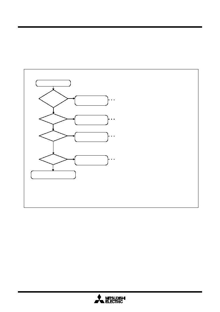
CPU Rewrite Mode (Flash Memory Version)
Mitsubishi microcomputers
M16C / 62A Group
SINGLE-CHIP 16-BIT CMOS MICROCOMPUTER
231
Read status register
SR4=1 and SR5
=1 ?
NO
Command
sequence error
YES
SR5=0?
YES
Block erase error
NO
SR4=0?
YES
Program error (page
or lock bit)
NO
SR3=0?
YES
Program error
(block)
NO
End (block erase, program)
Execute the clear status register command (50
16
)
to clear the status register. Try performing the
operation one more time after confirming that the
command is entered correctly.
Should a block erase error occur, the block in error
cannot be used.
Execute the read lock bit status command (71
16
)
to see if the block is locked. After removing lock,
execute write operation in the same way. If the
error still occurs, the page in error cannot be
used.
After erasing the block in error, execute write
operation one more time. If the same error still
occurs, the block in error cannot be used.
Note: When one of SR5 to SR3 is set to 1, none of the page program, block erase,
erase all unlock blocks and lock bit program commands is accepted. Execute the
clear status register command (50
16
) before executing these commands.
Full Status Check
By performing full status check, it is possible to know the execution results of erase and program
operations. Figure 1.26.8 shows a full status check flowchart and the action to be taken when each
error occurs.
Figure 1.26.8. Full status check flowchart and remedial procedure for errors

Functions To Inhibit Rewriting Flash Memory Version (Flash Memory Version)
Mitsubishi microcomputers
M16C / 62A Group
SINGLE-CHIP 16-BIT CMOS MICROCOMPUTER
232
Symbol
Address
When reset
ROMCP
0FFFFF
16
FF
16
ROM code protect level
2 set bit (Note 1, 2)
00: Protect enabled
01: Protect enabled
10: Protect enabled
11: Protect disabled
ROM code protect control address
Bit name
Function
Bit symbol
b7
b6
b5
b4
b3
b2
b1
b0
00: Protect removed
01: Protect set bit effective
10: Protect set bit effective
11: Protect set bit effective
00: Protect enabled
01: Protect enabled
10: Protect enabled
11: Protect disabled
ROM code protect reset
bit (Note 3)
ROM code protect level
1 set bit (Note 1)
ROMCP2
ROMCR
ROMCP1
b3 b2
b5 b4
b7 b6
Note 1: When ROM code protect is turned on, the on-chip flash memory is protected against
readout or modification in parallel input/output mode.
Note 2: When ROM code protect level 2 is turned on, ROM code readout by a shipment
inspection LSI tester, etc. also is inhibited.
Note 3: The ROM code protect reset bits can be used to turn off ROM code protect level 1 and
ROM code protect level 2. However, since these bits cannot be changed in parallel input/
output mode, they need to be rewritten in serial input/output or some other mode.
Reserved bit
Always set this bit to 1.
1 1
Functions To Inhibit Rewriting Flash Memory Version
To prevent the contents of the flash memory version from being read out or rewritten easily, the device
incorporates a ROM code protect function for use in parallel I/O mode and an ID code check function for
use in standard serial I/O mode.
ROM code protect function
The ROM code protect function is used to prohibit reading out or modifying the contents of the flash
memory during parallel I/O mode and is set by using the ROM code protect control address register
(0FFFFF
16
). Figure 1.27.1 shows the ROM code protect control address (0FFFFF
16
). (This address ex-
ists in the user ROM area.)
If one of the pair of ROM code protect bits is set to 0, ROM code protect is turned on, so that the contents
of the flash memory version are protected against readout and modification. ROM code protect is imple-
mented in two levels. If level 2 is selected, the flash memory is protected even against readout by a
shipment inspection LSI tester, etc. When an attempt is made to select both level 1 and level 2, level 2 is
selected by default.
If both of the two ROM code protect reset bits are set to "00," ROM code protect is turned off, so that the
contents of the flash memory version can be read out or modified. Once ROM code protect is turned on,
the contents of the ROM code protect reset bits cannot be modified in parallel I/O mode. Use the serial I/
O or some other mode to rewrite the contents of the ROM code protect reset bits.
Figure 1.27.1. ROM code protect control address

Functions To Inhibit Rewriting Flash Memory Version (Flash Memory Version)
Mitsubishi microcomputers
M16C / 62A Group
SINGLE-CHIP 16-BIT CMOS MICROCOMPUTER
233
ID Code Check Function
Use this function in standard serial I/O mode. When the contents of the flash memory are not blank, the ID
code sent from the peripheral unit is compared with the ID code written in the flash memory to see if they
match. If the ID codes do not match, the commands sent from the peripheral unit are not accepted. The ID
code consists of 8-bit data, the areas of which, beginning with the first byte, are 0FFFDF
16
, 0FFFE3
16
,
0FFFEB
16
, 0FFFEF
16
, 0FFFF3
16
, 0FFFF7
16
, and 0FFFFB
16
. Write a program which has had the ID code
preset at these addresses to the flash memory.
Figure 1.27.2. ID code store addresses
Reset vector
Watchdog timer vector
Single step vector
Address match vector
BRK instruction vector
Overflow vector
Undefined instruction vector
ID7
ID6
ID5
ID4
ID3
ID2
ID1
DBC vector
NMI vector
0FFFFC
16
to 0FFFFF
16
0FFFF8
16
to 0FFFFB
16
0FFFF4
16
to 0FFFF7
16
0FFFF0
16
to 0FFFF3
16
0FFFEC
16
to 0FFFEF
16
0FFFE8
16
to 0FFFEB
16
0FFFE4
16
to 0FFFE7
16
0FFFE0
16
to 0FFFE3
16
0FFFDC
16
to 0FFFDF
16
4 bytes
Address

Appendix Parallel I/O Mode (Flash Memory Version)
Mitsubishi microcomputers
M16C / 62A Group
SINGLE-CHIP 16-BIT CMOS MICROCOMPUTER
234
Parallel I/O Mode
The parallel I/O mode inputs and outputs the software commands, addresses and data needed to operate
(read, program, erase, etc.) the internal flash memory. This I/O is parallel.
Use an exclusive programer supporting M16C/62A (flash memory version).
Refer to the instruction manual of each programer maker for the details of use.
User ROM and Boot ROM Areas
In parallel I/O mode, the user ROM and boot ROM areas shown in Figure 1.25.1 can be rewritten. Both
areas of flash memory can be operated on in the same way.
Program and block erase operations can be performed in the user ROM area. The user ROM area and its
blocks are shown in Figure 1.25.1.
The boot ROM area is 8 Kbytes in size. In parallel I/O mode, it is located at addresses 0FE000
16
through
0FFFFF
16
. Make sure program and block erase operations are always performed within this address
range. (Access to any location outside this address range is prohibited.)
In the boot ROM area, an erase block operation is applied to only one 8 Kbyte block. The boot ROM area
has had a standard serial I/O mode control program stored in it when shipped from the Mitsubishi factory.
Therefore, using the device in standard serial input/output mode, you do not need to write to the boot
ROM area.

Appendix Standard Serial I/O Mode (Flash Memory Version)
Mitsubishi microcomputers
M16C / 62A Group
SINGLE-CHIP 16-BIT CMOS MICROCOMPUTER
235
Pin Description
V
CC
,V
SS
Apply program/erase protection voltage to Vcc pin and 0 V to Vss pin.
CNV
SS
Connect to Vcc pin.
RESET
Reset input pin. While reset is "L" level, a 20 cycle or longer clock
must be input to X
IN
pin.
X
IN
Connect a ceramic resonator or crystal oscillator between X
IN
and
X
OUT
pins. To input an externally generated clock, input it to X
IN
pin
and open X
OUT
pin.
X
OUT
BYTE
Connect this pin to V
SS
or V
CC
.
AV
CC
, AV
SS
V
REF
Connect AV
SS
to V
SS
and AV
CC
to V
CC
, respectively.
Enter the reference voltage for AD from this pin.
P0
0
to P0
7
Input "H" or "L" level signal or open.
P1
0
to P1
7
Input "H" or "L" level signal or open.
P2
0
to P2
7
Input "H" or "L" level signal or open.
P3
0
to P3
7
Input "H" or "L" level signal or open.
P4
0
to P4
7
Input "H" or "L" level signal or open.
P5
1
to P5
4,
P5
6,
P5
7
Input "H" or "L" level signal or open.
P5
0
Input "H" level signal.
P5
5
Input "L" level signal.
P6
0
to P6
3
Input "H" or "L" level signal or open.
P6
4
Standard serial I/O mode 1: BUSY signal output pin
Standard serial I/O mode 2: Monitors the boot program operation
check signal output pin.
P6
5
P6
6
Serial data input pin
P6
7
Serial data output pin
P7
0
to P7
7
Input "H" or "L" level signal or open.
P8
0
to P8
4
, P8
6
,
P8
7
Input "H" or "L" level signal or open.
P9
0
to P9
7
Input "H" or "L" level signal or open.
P10
0
to P10
7
Input "H" or "L" level signal or open.
Name
Power input
CNV
SS
Reset input
Clock input
Clock output
BYTE
Analog power supply input
Reference voltage input
Input port P0
Input port P1
Input port P2
Input port P3
Input port P4
Input port P5
CE input
EPM input
Input port P6
BUSY output
SCLK input
RxD input
TxD output
Input port P7
Input port P8
Input port P9
Input port P10
I/O
I
I
I
O
I
I
I
I
I
I
I
I
I
I
I
O
I
I
O
I
I
I
I
P8
5
NMI input
I
Connect this pin to Vcc.
Standard serial I/O mode 1: Serial clock input pin
Standard serial I/O mode 2: Input "L".
Pin functions (Flash memory standard serial I/O mode)

Appendix Standard Serial I/O Mode (Flash Memory Version)
Mitsubishi microcomputers
M16C / 62A Group
SINGLE-CHIP 16-BIT CMOS MICROCOMPUTER
236
Figure 1.29.1. Pin connections for serial I/O mode (1)
1
2 3
4 5
6
7
8 9 10 11 12 13 14 15 16 17 18 19 20 21 22 23 24 25 26 27 28 29 30
31
32
33
34
35
36
37
38
39
40
41
42
43
44
45
46
47
48
49
50
51
52
53
54
55
56
57
58
59
60
61
62
63
64
65
66
67
68
69
70
71
72
73
74
75
76
77
78
79
80
81
82
83
84
85
86
87
88
89
90
91
92
93
94
95
96
97
98
99
100
P0
0
/D
0
P0
1
/D
1
P0
2
/D
2
P0
3
/D
3
P0
4
/D
4
P0
5
/D
5
P0
6
/D
6
P0
7
/D
7
P1
0
/D
8
P1
1
/D
9
P1
2
/D
10
P1
3
/D
11
P1
4
/D
12
P1
5
/D
13
/INT3
V
REF
AV
SS
P1
6
/D
14
/INT4
P1
7
/D
15
/INT5
V
CC
X
IN
X
OUT
V
SS
RESET
CNVss
P8
7
/X
CIN
P8
6
/X
COUT
BYTE
P2
0
/A
0
(/D
0
/-)
P2
1
/A
1
(/D
1
/D
0
)
P2
2
/A
2
(/D
2
/D
1
)
P2
3
/A
3
(/D
3
/D
2
)
P2
4
/A
4
(/D
4
/D
3
)
P2
5
/A
5
(/D
5
/D
4
)
P2
6
/A
6
(/D
6
/D
5
)
P2
7
/A
7
(/D
7
/D
6
)
P3
0
/A
8
(/-/D
7
)
P3
1
/A
9
P3
2
/A
10
P3
3
/A
11
P3
4
/A
12
P3
5
/A
13
P3
6
/A
14
P3
7
/A
15
P4
0
/A
16
P4
1
/A
17
P4
2
/A
18
P4
3
/A
19
P7
4
/TA2
OUT
/W
P7
5
/TA2
IN
/W
P7
6
/TA3
OUT
P5
6
/ALE
P7
7
/TA3
IN
P5
5
/HOLD
P5
4
/HLDA
P5
3
/BCLK
P5
2
/RD
Vcc
Vss
P5
7
/RDY/CLK
OUT
P4
5
/CS1
P4
6
/CS2
P4
7
/CS3
AVcc
P6
3
/T
X
D
0
P6
5
/CLK
1
P6
6
/RxD
1
P6
7
/T
X
D
1
P6
1
/CLK
0
P6
2
/RxD
0
P10
0
/AN
0
P10
1
/AN
1
P10
2
/AN
2
P10
3
/AN
3
P10
4
/AN
4/
KI
0
P10
5
/AN
5
/KI
1
P10
6
/AN
6
/KI
2
P10
7
/AN
7
/KI
3
P9
3
/DA
0
/TB3
IN
P9
4
/DA
1
/TB4
IN
P9
5
/ANEX0/CLK4
P9
6
/ANEX1/S
OUT
4
P9
1
/TB1
IN
/S
IN
3
P9
2
/TB2
IN
/S
OUT
3
P9
7
/AD
TRG
/S
IN
4
P8
2
/INT
0
P8
3
/INT
1
P8
1
/TA4
IN
/U
P8
4
/INT
2
P8
0
/TA4
OUT
/U
P6
0
/CTS
0
/RTS
0
P6
4
/CTS
1
/RTS
1
/CTS
0
/CLKS
1
P7
3
/CTS
2
/RTS
2
/TA1
IN
/V
P7
2
/CLK
2
/TA1
OUT
/V
P7
1
/RxD
2
/SCL/TA0
IN
/TB5
IN
P8
5
/NMI
P4
4
/CS0
P5
0
/WRL/WR
P5
1
/WRH/BHE
P9
0
/TB0
IN
/CLK3
P7
0
/T
X
D
2
/SDA/TA0
OUT
Vcc
Vss
RxD
TxD
SCLK
CNVss
CE
EPM
BUSY
RESET
Connect
oscillator
circuit.
CNVss
Vcc
EPM
Vss
RESET
Vss to Vcc
CE
Vcc
Signal
Value
Mode setup method
Package: 100P6S-A
M16C/62A Group
(Flash memory version)

Appendix Standard Serial I/O Mode (Flash Memory Version)
Mitsubishi microcomputers
M16C / 62A Group
SINGLE-CHIP 16-BIT CMOS MICROCOMPUTER
237
Figure 1.29.2. Pin connections for serial I/O mode (2)
CNVss
Vcc
EPM
Vss
RESET
Vss to Vcc
CE
Vcc
Signal
Value
Mode setup method
CNV
SS
RESET
V
SS
V
CC
CE
1 2
3
4
5
6 7
8
9 10 11 12 13 14 15 16 17 18 19 20 21 22 23 24 25
26
27
28
29
30
31
32
33
34
35
36
37
38
39
40
41
42
43
44
45
46
47
48
49
50
100
99
98
97
96
95
94
93
92
91
90
89
88
87
86
85
84
83
82
81
80
79
78
77
76
75 74 73 72 71 70 69 68 67 66 65 64 63 62 61 60 59 58 57 56 55 54 53 52 51
P6
4
/CTS
1
/RTS
1
/CTS
0
/CLKS
1
P4
2
/A
18
P4
3
/A
19
P5
6
/ALE
P5
5
/HOLD
P5
4
/HLDA
P5
3
/BCLK
P5
2
/RD
P5
7
/RDY/CLK
OUT
P4
5
/CS1
P4
6
/CS2
P4
7
/CS3
P6
3
/T
X
D
0
P6
5
/CLK
1
P6
6
/RxD
1
P6
7
/T
X
D
1
P6
1
/CLK
0
P6
2
/RxD
0
P6
0
/CTS
0
/RTS
0
P4
4
/CS0
P5
0
/WRL/WR
P5
1
/WRH/BHE
P7
2
/CLK
2
/TA1
OUT
/V
P7
1
/RxD
2
/SCL/TA0
IN
/TB5
IN
P7
0
/T
X
D
2
/SDA/TA0
OUT
P0
7
/D
7
P1
0
/D
8
P1
1
/D
9
P1
2
/D
10
V
REF
AV
SS
AVcc
P10
0
/AN
0
P10
1
/AN
1
P10
2
/AN
2
P10
3
/AN
3
P9
5
/ANEX0/CLK4
P9
6
/ANEX1/S
OUT
4
P9
7
/AD
TRG
/S
IN
4
P10
7
/AN
7
/KI
3
P10
6
/AN
6
/KI
2
P10
5
/AN
5
/KI
1
P10
4
/AN
4/
KI
0
P1
3
/D
11
P1
4
/D
12
P2
0
/A
0
(/D
0
/-)
P2
1
/A
1
(/D
1
/D
0
)
P2
2
/A
2
(/D
2
/D
1
)
P2
3
/A
3
(/D
3
/D
2
)
P2
4
/A
4
(/D
4
/D
3
)
P2
5
/A
5
(/D
5
/D
4
)
P2
6
/A
6
(/D
6
/D
5
)
P2
7
/A
7
(/D
7
/D
6
)
P3
0
/A
8
(/-/D
7
)
P3
1
/A
9
P3
2
/A
10
P3
3
/A
11
P3
4
/A
12
P3
5
/A
13
P3
6
/A
14
P3
7
/A
15
P4
0
/A
16
P4
1
/A
17
Vcc
Vss
P1
5
/D
13
/INT
3
P1
6
/D
14
/INT
4
P1
7
/D
15
/INT
5
P7
4
/TA2
OUT
/W
V
CC
X
IN
X
OUT
V
SS
RESET
CNVss
P8
7
/X
CIN
P8
6
/X
COUT
BYTE
P7
6
/TA3
OUT
P7
7
/TA3
IN
P9
3
/DA
0
/TB3
IN
P9
4
/DA
1
/TB4
IN
P9
1
/TB1
IN
/S
IN
3
P9
2
/TB2
IN
/S
OUT
3
P8
0
/TA4
OUT
/U
P8
2
/INT
0
P8
3
/INT
1
P8
5
/NMI
P9
0
/TB0
IN
/CLK3
P8
4
/INT
2
P7
5
/TA2
IN
/W
P8
1
/TA4
IN
/U
P7
3
/CTS
2
/RTS
2
/TA1
IN
/V
BUSY
EPM
SCLK
R
X
D
T
X
D
Connect
oscillator
circuit.
P0
6
/D
6
P0
5
/D
5
P0
4
/D
4
P0
3
/D
3
P0
2
/D
2
P0
1
/D
1
P0
0
/D
0
Package: 100P6Q-A
M16C/62A Group
(Flash memory version)

Appendix Standard Serial I/O Mode (Flash Memory Version)
Mitsubishi microcomputers
M16C / 62A Group
SINGLE-CHIP 16-BIT CMOS MICROCOMPUTER
238
Standard serial I/O mode
The standard serial I/O mode inputs and outputs the software commands, addresses and data needed to
operate (read, program, erase, etc.) the internal flash memory. This I/O is serial. There are actually two
standard serial I/O modes: mode 1, which is clock synchronized, and mode 2, which is asynchronized. Both
modes require a purpose-specific peripheral unit.
The standard serial I/O mode is different from the parallel I/O mode in that the CPU controls flash memory
rewrite (uses the CPU's rewrite mode), rewrite data input and so forth. It is started when the reset is re-
_____
________
leased, which is done when the P5
0
(CE) pin is "H" level, the P5
5
(EPM) pin "L" level and the CNVss pin "H"
level. (In the ordinary command mode, set CNVss pin to "L" level.)
This control program is written in the boot ROM area when the product is shipped from Mitsubishi. Accord-
ingly, make note of the fact that the standard serial I/O mode cannot be used if the boot ROM area is
rewritten in the parallel I/O mode. Figures 1.29.1 and 1.29.2 show the pin connections for the standard
serial I/O mode. Serial data I/O uses UART1 and transfers the data serially in 8-bit units. Standard serial I/
O switches between mode 1 (clock synchronized) and mode 2 (clock asynchronized) according to the level
of CLK
1
pin when the reset is released.
To use standard serial I/O mode 1 (clock synchronized), set the CLK
1
pin to "H" level and release the reset.
The operation uses the four UART1 pins CLK
1
, RxD
1
, TxD
1
and RTS
1
(BUSY). The CLK
1
pin is the transfer
clock input pin through which an external transfer clock is input. The TxD
1
pin is for CMOS output. The
RTS
1
(BUSY) pin outputs an "L" level when ready for reception and an "H" level when reception starts.
To use standard serial I/O mode 2 (clock asynchronized), set the CLK
1
pin to "L" level and release the
reset. The operation uses the two UART1 pins RxD
1
and TxD
1
.
In the standard serial I/O mode, only the user ROM area indicated in Figure 1.29.19 can be rewritten. The
boot ROM cannot.
In the standard serial I/O mode, a 7-byte ID code is used. When there is data in the flash memory, com-
mands sent from the peripheral unit are not accepted unless the ID code matches.

Appendix Standard Serial I/O Mode 1 (Flash Memory Version)
Mitsubishi microcomputers
M16C / 62A Group
SINGLE-CHIP 16-BIT CMOS MICROCOMPUTER
239
Overview of standard serial I/O mode 1 (clock synchronized)
In standard serial I/O mode 1, software commands, addresses and data are input and output between the
MCU and peripheral units (serial programer, etc.) using 4-wire clock-synchronized serial I/O (UART1).
Standard serial I/O mode 1 is engaged by releasing the reset with the P6
5
(CLK
1
) pin "H" level.
In reception, software commands, addresses and program data are synchronized with the rise of the
transfer clock that is input to the CLK
1
pin, and are then input to the MCU via the RxD
1
pin. In transmis-
sion, the read data and status are synchronized with the fall of the transfer clock, and output from the
TxD
1
pin.
The TxD
1
pin is for CMOS output. Transfer is in 8-bit units with LSB first.
When busy, such as during transmission, reception, erasing or program execution, the RTS
1
(BUSY) pin
is "H" level. Accordingly, always start the next transfer after the RTS
1
(BUSY) pin is "L" level.
Also, data and status registers in memory can be read after inputting software commands. Status, such
as the operating state of the flash memory or whether a program or erase operation ended successfully or
not, can be checked by reading the status register. Here following are explained software commands,
status registers, etc.
Appendix Standard Serial I/O Mode 1 (Flash Memory Version)
Mitsubishi microcomputers
M16C / 62A Group
SINGLE-CHIP 16-BIT CMOS MICROCOMPUTER
240
Software Commands
Table 1.29.1 lists software commands. In the standard serial I/O mode 1, erase operations, programs and
reading are controlled by transferring software commands via the RxD
1
pin. Software commands are
explained here below.
Table 1.29.1. Software commands (Standard serial I/O mode 1)
Control command
2nd byte 3rd byte 4th byte 5th byte 6th byte
1
Page read
2
Page program
3
Block erase
4
Erase all unlocked blocks
5
Read status register
6
Clear status register
7
Read lock bit status
8
Lock bit program
9
Lock bit enable
10
Lock bit disable
11
ID check function
12
Download function
13
Version data output function
14
Boot ROM area output
function
15
Read check data
Address
(middle)
Address
(middle)
Address
(middle)
D0
16
SRD
output
Address
(middle)
Address
(middle)
Address
(low)
Size (low)
Version
data
output
Address
(middle)
Check
data (low)
Address
(high)
Address
(high)
Address
(high)
SRD1
output
Address
(high)
Address
(high)
Address
(middle)
Size
(high)
Version
data
output
Address
(high)
Check
data
(high)
Data
output
Data
input
D0
16
Lock bit
data
output
D0
16
Address
(high)
Check-
sum
Version
data
output
Data
output
Data
output
Data
input
ID size
Data
input
Version
data
output
Data
output
Data
output
Data
input
ID1
To
required
number
of times
Version
data
output
Data
output
Data
output to
259th byte
Data input
to 259th
byte
To ID7
Version
data
output to
9th byte
Data
output to
259th
byte
FF
16
41
16
20
16
A7
16
70
16
50
16
71
16
77
16
7A
16
75
16
F5
16
FA
16
FB
16
FC
16
FD
16
When ID is
not verified
Not
acceptable
Not
acceptable
Not
acceptable
Not
acceptable
Acceptable
Not
acceptable
Not
acceptable
Not
acceptable
Not
acceptable
Not
acceptable
Acceptable
Not
acceptable
Acceptable
Not
acceptable
Not
acceptable
1st byte
transfer
Note 1: Shading indicates transfer from flash memory microcomputer to peripheral unit. All other data is trans-
ferred from the peripheral unit to the flash memory microcomputer.
Note 2: SRD refers to status register data. SRD1 refers to status register 1 data.
Note 3: All commands can be accepted when the flash memory is totally blank.
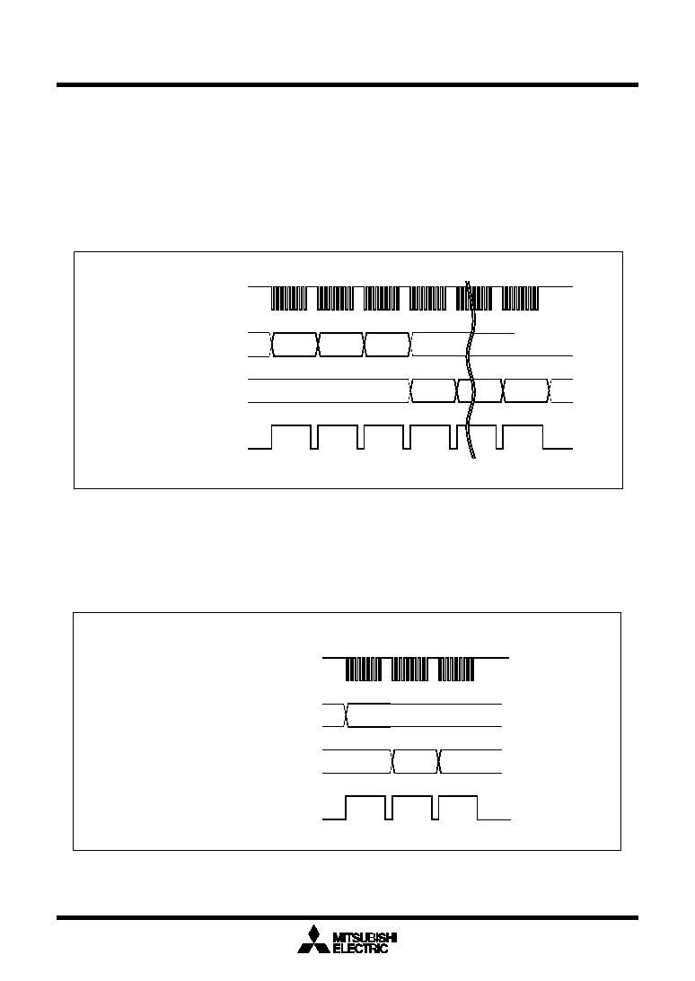
Appendix Standard Serial I/O Mode 1 (Flash Memory Version)
Mitsubishi microcomputers
M16C / 62A Group
SINGLE-CHIP 16-BIT CMOS MICROCOMPUTER
241
Page Read Command
This command reads the specified page (256 bytes) in the flash memory sequentially one byte at a
time. Execute the page read command as explained here following.
(1) Transfer the "FF
16
" command code with the 1st byte.
(2) Transfer addresses A
8
to A
15
and A
16
to A
23
with the 2nd and 3rd bytes respectively.
(3) From the 4th byte onward, data (D
0
≠D
7
) for the page (256 bytes) specified with addresses A
8
to
A
23
will be output sequentially from the smallest address first in sync with the fall of the clock.
Figure 1.29.3. Timing for page read
Read Status Register Command
This command reads status information. When the "70
16
" command code is sent with the 1st byte, the
contents of the status register (SRD) specified with the 2nd byte and the contents of status register 1
(SRD1) specified with the 3rd byte are read.
Figure 1.29.4. Timing for reading the status register
data0
data255
CLK1
RxD1
TxD1
RTS1(BUSY)
A
8
to
A
15
A
16
to
A
23
FF
16
(M16C reception data)
(M16C transmit data)
SRD
output
SRD1
output
CLK1
RxD1
TxD1
RTS1(BUSY)
70
16
(M16C reception data)
(M16C transmit data)

Appendix Standard Serial I/O Mode 1 (Flash Memory Version)
Mitsubishi microcomputers
M16C / 62A Group
SINGLE-CHIP 16-BIT CMOS MICROCOMPUTER
242
Clear Status Register Command
This command clears the bits (SR3≠SR5) which are set when the status register operation ends in
error. When the "50
16
" command code is sent with the 1st byte, the aforementioned bits are cleared.
When the clear status register operation ends, the RTS
1
(BUSY) signal changes from the "H" to the
"L" level.
Figure 1.29.5. Timing for clearing the status register
Page Program Command
This command writes the specified page (256 bytes) in the flash memory sequentially one byte at a
time. Execute the page program command as explained here following.
(1) Transfer the "41
16
" command code with the 1st byte.
(2) Transfer addresses A
8
to A
15
and A
16
to A
23
with the 2nd and 3rd bytes respectively.
(3) From the 4th byte onward, as write data (D
0
≠D
7
) for the page (256 bytes) specified with addresses
A
8
to A
23
is input sequentially from the smallest address first, that page is automatically written.
When reception setup for the next 256 bytes ends, the RTS
1
(BUSY) signal changes from the "H" to
the "L" level. The result of the page program can be known by reading the status register. For more
information, see the section on the status register.
Each block can be write-protected with the lock bit. For more information, see the section on the data
protection function. Additional writing is not allowed with already programmed pages.
Figure 1.29.6. Timing for the page program
CLK1
RxD1
TxD1
RTS1(BUSY)
50
16
(M16C reception data)
(M16C transmit data)
CLK1
RxD1
TxD1
RTS1(BUSY)
A
8
to
A
15
A
16
to
A
23
41
16
data0
data255
(M16C reception data)
(M16C transmit data)

Appendix Standard Serial I/O Mode 1 (Flash Memory Version)
Mitsubishi microcomputers
M16C / 62A Group
SINGLE-CHIP 16-BIT CMOS MICROCOMPUTER
243
Block Erase Command
This command erases the data in the specified block. Execute the block erase command as explained
here following.
(1) Transfer the "20
16
" command code with the 1st byte.
(2) Transfer addresses A
8
to A
15
and A
16
to A
23
with the 2nd and 3rd bytes respectively.
(3) Transfer the verify command code "D0
16
" with the 4th byte. With the verify command code, the
erase operation will start for the specified block in the flash memory. Write the highest address of
the specified block for addresses A
8
to A
23
.
When block erasing ends, the RTS
1
(BUSY) signal changes from the "H" to the "L" level. After block
erase ends, the result of the block erase operation can be known by reading the status register. For
more information, see the section on the status register.
Each block can be erase-protected with the lock bit. For more information, see the section on the data
protection function.
Figure 1.29.7. Timing for block erasing
A
8
to
A
15
A
16
to
A
23
20
16
D0
16
CLK1
RxD1
TxD1
RTS1(BUSY)
(M16C reception data)
(M16C transmit data)

Appendix Standard Serial I/O Mode 1 (Flash Memory Version)
Mitsubishi microcomputers
M16C / 62A Group
SINGLE-CHIP 16-BIT CMOS MICROCOMPUTER
244
Erase All Unlocked Blocks Command
This command erases the content of all blocks. Execute the erase all unlocked blocks command as
explained here following.
(1) Transfer the "A7
16
" command code with the 1st byte.
(2) Transfer the verify command code "D0
16
" with the 2nd byte. With the verify command code, the
erase operation will start and continue for all blocks in the flash memory.
When block erasing ends, the RTS
1
(BUSY) signal changes from the "H" to the "L" level. The result of the
erase operation can be known by reading the status register. Each block can be erase-protected with the
lock bit. For more information, see the section on the data protection function.
Figure 1.29.8. Timing for erasing all unlocked blocks
Lock Bit Program Command
This command writes "0" (lock) for the lock bit of the specified block. Execute the lock bit program
command as explained here following.
(1) Transfer the "77
16
" command code with the 1st byte.
(2) Transfer addresses A
8
to A
15
and A
16
to A
23
with the 2nd and 3rd bytes respectively.
(3) Transfer the verify command code "D0
16
" with the 4th byte. With the verify command code, "0" is
written for the lock bit of the specified block. Write the highest address of the specified block for
addresses A
8
to A
23
.
When writing ends, the RTS
1
(BUSY) signal changes from the "H" to the "L" level. Lock bit status can
be read with the read lock bit status command. For information on the lock bit function, reset proce-
dure and so on, see the section on the data protection function.
Figure 1.29.9. Timing for the lock bit program
CLK1
RxD1
TxD1
RTS1(BUSY)
A7
16
D0
16
(M16C reception data)
(M16C transmit data)
CLK1
RxD1
TxD1
RTS1(BUSY)
A
8
to
A
15
A
16
to
A
23
77
16
D0
16
(M16C reception data)
(M16C transmit data)

Appendix Standard Serial I/O Mode 1 (Flash Memory Version)
Mitsubishi microcomputers
M16C / 62A Group
SINGLE-CHIP 16-BIT CMOS MICROCOMPUTER
245
Lock Bit Enable Command
This command enables the lock bit in blocks whose bit was disabled with the lock bit disable com-
mand. The command code "7A
16
" is sent with the 1st byte of the serial transmission. This command
only enables the lock bit function; it does not set the lock bit itself.
Read Lock Bit Status Command
This command reads the lock bit status of the specified block. Execute the read lock bit status com-
mand as explained here following.
(1) Transfer the "71
16
" command code with the 1st byte.
(2) Transfer addresses A
8
to A
15
and A
16
to A
23
with the 2nd and 3rd bytes respectively.
(3) The lock bit data of the specified block is output with the 4th byte. The lock bit data is the 6th
bit(D
6
) of the output data. Write the highest address of the specified block for addresses A
8
to
A
23
.
Figure 1.29.10. Timing for reading lock bit status
Figure 1.29.11. Timing for enabling the lock bit
CLK1
RxD1
TxD1
RTS1(BUSY)
A
8
to
A
15
A
16
to
A
23
71
16
D
6
(M16C reception data)
(M16C transmit data)
7A
16
CLK1
RxD1
TxD1
RTS1(BUSY)
(M16C reception data)
(M16C transmit data)

Appendix Standard Serial I/O Mode 1 (Flash Memory Version)
Mitsubishi microcomputers
M16C / 62A Group
SINGLE-CHIP 16-BIT CMOS MICROCOMPUTER
246
Lock Bit Disable Command
This command disables the lock bit. The command code "75
16
" is sent with the 1st byte of the serial
transmission. This command only disables the lock bit function; it does not set the lock bit itself.
However, if an erase command is executed after executing the lock bit disable command, "0" (locked)
lock bit data is set to "1" (unlocked) after the erase operation ends. In any case, after the reset is
cancelled, the lock bit is enabled.
Figure 1.29.12. Timing for disabling the lock bit
Download Command
This command downloads a program to the RAM for execution. Execute the download command as
explained here following.
(1) Transfer the "FA
16
" command code with the 1st byte.
(2) Transfer the program size with the 2nd and 3rd bytes.
(3) Transfer the check sum with the 4th byte. The check sum is added to all data sent with the 5th
byte onward.
(4) The program to execute is sent with the 5th byte onward.
When all data has been transmitted, if the check sum matches, the downloaded program is executed.
The size of the program will vary according to the internal RAM.
Figure 1.29.13. Timing for download
75
16
CLK1
RxD1
TxD1
RTS1(BUSY)
(M16C reception data)
(M16C transmit data)
FA
16
Program
data
Program
data
Data size (high)
Data size (low)
Check
sum
CLK1
RxD1
TxD1
RTS1(BUSY)
(M16C reception data)
(M16C transmit data)

Appendix Standard Serial I/O Mode 1 (Flash Memory Version)
Mitsubishi microcomputers
M16C / 62A Group
SINGLE-CHIP 16-BIT CMOS MICROCOMPUTER
247
Version Information Output Command
This command outputs the version information of the control program stored in the boot area. Execute
the version information output command as explained here following.
(1) Transfer the "FB
16
" command code with the 1st byte.
(2) The version information will be output from the 2nd byte onward. This data is composed of 8
ASCII code characters.
Figure 1.29.14. Timing for version information output
Boot ROM Area Output Command
This command outputs the control program stored in the boot ROM area in one page blocks (256
bytes). Execute the boot ROM area output command as explained here following.
(1) Transfer the "FC
16
" command code with the 1st byte.
(2) Transfer addresses A
8
to A
15
and A
16
to A
23
with the 2nd and 3rd bytes respectively.
(3) From the 4th byte onward, data (D
0
≠D
7
) for the page (256 bytes) specified with addresses A
8
to
A
23
will be output sequentially from the smallest address first, in sync with the fall of the clock.
Figure 1.29.15. Timing for boot ROM area output
FB
16
'X'
'V'
'E'
'R'
CLK1
RxD1
TxD1
RTS1(BUSY)
(M16C reception data)
(M16C transmit data)
data0
data255
CLK1
RxD1
TxD1
RTS1(BUSY)
A
8
to
A
15
A
16
to
A
23
FC
16
(M16C reception data)
(M16C transmit data)

Appendix Standard Serial I/O Mode 1 (Flash Memory Version)
Mitsubishi microcomputers
M16C / 62A Group
SINGLE-CHIP 16-BIT CMOS MICROCOMPUTER
248
ID Check
This command checks the ID code. Execute the boot ID check command as explained here following.
(1) Transfer the "F5
16
" command code with the 1st byte.
(2) Transfer addresses A
0
to A
7
, A
8
to A
15
and A
16
to A
23
of the 1st byte of the ID code with the 2nd,
3rd and 4th bytes respectively.
(3) Transfer the number of data sets of the ID code with the 5th byte.
(4) The ID code is sent with the 6th byte onward, starting with the 1st byte of the code.
Figure 1.29.16. Timing for the ID check
ID Code
When the flash memory is not blank, the ID code sent from the peripheral units and the ID code written
in the flash memory are compared to see if they match. If the codes do not match, the command sent
from the peripheral units is not accepted. An ID code contains 8 bits of data. Area is, from the 1st byte,
addresses 0FFFDF
16
, 0FFFE3
16
, 0FFFEB
16
, 0FFFEF
16
, 0FFFF3
16
, 0FFFF7
16
and 0FFFFB
16
. Write
a program into the flash memory, which already has the ID code set for these addresses.
Figure 1.29.17. ID code storage addresses
ID size
ID1
ID7
CLK1
RxD1
TxD1
RTS1(BUSY)
F5
16
DF
16
FF
16
0F
16
(M16C reception
data)
(M16C transmit
data)
Reset vector
Watchdog timer vector
Single step vector
Address match vector
BRK instruction vector
Overflow vector
Undefined instruction vector
ID7
ID6
ID5
ID4
ID3
ID2
ID1
DBC vector
NMI vector
0FFFFC
16
to 0FFFFF
16
0FFFF8
16
to 0FFFFB
16
0FFFF4
16
to 0FFFF7
16
0FFFF0
16
to 0FFFF3
16
0FFFEC
16
to 0FFFEF
16
0FFFE8
16
to 0FFFEB
16
0FFFE4
16
to 0FFFE7
16
0FFFE0
16
to 0FFFE3
16
0FFFDC
16
to 0FFFDF
16
4 bytes
Address

Appendix Standard Serial I/O Mode 1 (Flash Memory Version)
Mitsubishi microcomputers
M16C / 62A Group
SINGLE-CHIP 16-BIT CMOS MICROCOMPUTER
249
Read Check Data
This command reads the check data that confirms that the write data, which was sent with the page
program command, was successfully received.
(1) Transfer the "FD
16
" command code with the 1st byte.
(2) The check data (low) is received with the 2nd byte and the check data (high) with the 3rd.
To use this read check data command, first execute the command and then initialize the check data.
Next, execute the page program command the required number of times. After that, when the read
check command is executed again, the check data for all of the read data that was sent with the page
program command during this time is read. The check data is the result of CRC operation of write
data.
Figure 1.29.18. Timing for the read check data
Check data (low)
CLK1
RxD1
TxD1
RTS1(BUSY)
FD
16
(M16C reception data)
(M16C transmit data)
Check data (high)

Appendix Standard Serial I/O Mode 1 (Flash Memory Version)
Mitsubishi microcomputers
M16C / 62A Group
SINGLE-CHIP 16-BIT CMOS MICROCOMPUTER
250
Data Protection (Block Lock)
Each of the blocks in Figure 1.29.19 have a nonvolatile lock bit that specifies protection (block lock)
against erasing/writing. A block is locked (writing "0" for the lock bit) with the lock bit program command.
Also, the lock bit of any block can be read with the read lock bit status command.
Block lock disable/enable is determined by the status of the lock bit itself and execution status of the lock
bit disable and lock enable bit commands.
(1) After the reset has been cancelled and the lock bit enable command executed, the specified block
can be locked/unlocked using the lock bit (lock bit data). Blocks with a "0" lock bit data are locked
and cannot be erased or written in. On the other hand, blocks with a "1" lock bit data are unlocked
and can be erased or written in.
(2) After the lock bit disable command has been executed, all blocks are unlocked regardless of lock bit
data status and can be erased or written in. In this case, lock bit data that was "0" (locked) before the
block was erased is set to "1" (unlocked) after erasing, therefore the block is actually unlocked with
the lock bit.
Figure 1.29.19. Blocks in the user area
0C0000
16
0D0000
16
Block 6 : 64K byte
Block 5 : 64K byte
0E0000
16
Block 4 : 64K byte
0F0000
16
Block 3 : 32K byte
0F8000
16
Block 2 : 8K byte
0FA000
16
Block 1 : 8K byte
Block 0 : 16K byte
0FC000
16
User ROM area
0FFFFF
16
Flash memory
size
Flash memory
start address
256Kbytes
0C0000
16
128Kbytes
0E0000
16

Appendix Standard Serial I/O Mode 1 (Flash Memory Version)
Mitsubishi microcomputers
M16C / 62A Group
SINGLE-CHIP 16-BIT CMOS MICROCOMPUTER
251
Status Register (SRD)
The status register indicates operating status of the flash memory and status such as whether an erase
operation or a program ended successfully or in error. It can be read by writing the read status register
command (70
16
). Also, the status register is cleared by writing the clear status register command (50
16
).
Table 1.29.2 gives the definition of each status register bit. After clearing the reset, the status register
outputs "80
16
".
Table 1.29.2. Status register (SRD)
Write State Machine (WSM) Status (SR7)
The write state machine (WSM) status indicates the operating status of the flash memory. When
power is turned on, "1" (ready) is set for it. The bit is set to "0" (busy) during an auto write or auto erase
operation, but it is set back to "1" when the operation ends.
Erase Status (SR5)
The erase status reports the operating status of the auto erase operation. If an erase error occurs, it is
set to "1". When the erase status is cleared, it is set to "0".
Program Status (SR4)
The program status reports the operating status of the auto write operation. If a write error occurs, it is
set to "1". When the program status is cleared, it is set to "0".
Block Status After Program (SR3)
If excessive data is written (phenomenon whereby the memory cell becomes depressed which results
in data not being read correctly), "1" is set for the block status after-program at the end of the page
write operation. In other words, when writing ends successfully, "80
16
" is output; when writing fails,
"90
16
" is output; and when excessive data is written, "88
16
" is output.
If "1" is written for any of the SR5, SR4 or SR3 bits, the page program, block erase, erase all unlocked
blocks and lock bit program commands are not accepted. Before executing these commands, execute
the clear status register command (50
16
) and clear the status register.
SRD0 bits
SR7 (bit7)
SR6 (bit6)
SR5 (bit5)
SR4 (bit4)
SR3 (bit3)
SR2 (bit2)
SR1 (bit1)
SR0 (bit0)
Status name
Write state machine (WSM) status
Reserved
Erase status
Program status
Block status after program
Reserved
Reserved
Reserved
Definition
"1" "0"
Ready
-
Terminated in error
Terminated in error
Terminated in error
-
-
-
Busy
-
Terminated normally
Terminated normally
Terminated normally
-
-
-

Appendix Standard Serial I/O Mode 1 (Flash Memory Version)
Mitsubishi microcomputers
M16C / 62A Group
SINGLE-CHIP 16-BIT CMOS MICROCOMPUTER
252
Status Register 1 (SRD1)
Status register 1 indicates the status of serial communications, results from ID checks and results from
check sum comparisons. It can be read after the SRD by writing the read status register command (70
16
).
Also, status register 1 is cleared by writing the clear status register command (50
16
).
Table 1.29.3 gives the definition of each status register 1 bit. "00
16
" is output when power is turned ON
and the flag status is maintained even after the reset.
Table 1.29.3. Status register 1 (SRD1)
Boot Update Completed Bit (SR15)
This flag indicates whether the control program was downloaded to the RAM or not, using the down-
load function.
Check Sum Match Bit (SR12)
This flag indicates whether the check sum matches or not when a program, is downloaded for execu-
tion using the download function.
ID Check Completed Bits (SR11 and SR10)
These flags indicate the result of ID checks. Some commands cannot be accepted without an ID
check.
Data Receive Time Out (SR9)
This flag indicates when a time out error is generated during data reception. If this flag is attached
during data reception, the received data is discarded and the microcomputer returns to the command
wait state.
SRD1 bits
SR15 (bit7)
SR14 (bit6)
SR13 (bit5)
SR12 (bit4)
SR11 (bit3)
SR10 (bit2)
SR9 (bit1)
SR8 (bit0)
Status name
Boot update completed bit
Reserved
Reserved
Check sum match bit
ID check completed bits
Data receive time out
Reserved
Definition
"1" "0"
Update co
mpleted
-
-
Match
00
01
10
11
Not update
-
-
Mismatch
Normal operation
-
Not verified
Verification mismatch
Reserved
Verified
Time out
-

Appendix Standard Serial I/O Mode 1 (Flash Memory Version)
Mitsubishi microcomputers
M16C / 62A Group
SINGLE-CHIP 16-BIT CMOS MICROCOMPUTER
253
Full Status Check
Results from executed erase and program operations can be known by running a full status check. Figure
1.29.20 shows a flowchart of the full status check and explains how to remedy errors which occur.
Read status register
SR4=1 and SR5
=1 ?
NO
Command
sequence error
YES
SR5=0?
YES
Block erase error
NO
SR4=0?
YES
Program error (page
or lock bit)
NO
SR3=0?
YES
Program error
(block)
NO
End (block erase, program)
Execute the clear status register command (50
16
)
to clear the status register. Try performing the
operation one more time after confirming that the
command is entered correctly.
Should a block erase error occur, the block in error
cannot be used.
Execute the read lock bit status command (71
16
)
to see if the block is locked. After removing lock,
execute write operation in the same way. If the
error still occurs, the page in error cannot be
used.
After erasing the block in error, execute write
operation one more time. If the same error still
occurs, the block in error cannot be used.
Note: When one of SR5 to SR3 is set to 1, none of the page program, block erase,
erase all unlock blocks and lock bit program commands is accepted. Execute the
clear status register command (50
16
) before executing these commands.
Figure 1.29.20. Full status check flowchart and remedial procedure for errors

Appendix Standard Serial I/O Mode 1 (Flash Memory Version)
Mitsubishi microcomputers
M16C / 62A Group
SINGLE-CHIP 16-BIT CMOS MICROCOMPUTER
254
Example Circuit Application for The Standard Serial I/O Mode 1
The below figure shows a circuit application for the standard serial I/O mode 1. Control pins will vary
according to programmer, therefore see the peripheral unit manual for more information.
Figure 1.29.21. Example circuit application for the standard serial I/O mode 1
RTS1(BUSY)
CLK1
R
X
D1
T
X
D1
CNVss
Clock input
BUSY output
Data input
Data output
P5
0
(CE)
P5
5
(EPM)
(1) Control pins and external circuitry will vary according to peripheral unit.
For more information, see the peripheral unit manual.
(2) In this example, the microprocessor mode and standard serial I/O mode
are switched via a switch.
NMI
M16C/62A Group
(Flash memory version)

Appendix Standard Serial I/O Mode 2 (Flash Memory Version)
Mitsubishi microcomputers
M16C / 62A Group
SINGLE-CHIP 16-BIT CMOS MICROCOMPUTER
255
Overview of standard serial I/O mode 2 (clock asynchronized)
In standard serial I/O mode 2, software commands, addresses and data are input and output between the
MCU and peripheral units (serial programer, etc.) using 2-wire clock-asynchronized serial I/O (UART1).
Standard serial I/O mode 2 is engaged by releasing the reset with the P6
5
(CLK
1
) pin "L" level.
The TxD
1
pin is for CMOS output. Data transfer is in 8-bit units with LSB first, 1 stop bit and parity OFF.
After the reset is released, connections can be established at 9,600 bps when initial communications (Fig-
ure 1.29.22) are made with a peripheral unit. However, this requires a main clock with a minimum 2 MHz
input oscillation frequency. Baud rate can also be changed from 9,600 bps to 19,200, 38,400 or 57,600 bps
by executing software commands. However, communication errors may occur because of the oscillation
frequency of the main clock. If errors occur, change the main clock's oscillation frequency and the baud
rate.
After executing commands from a peripheral unit that requires time to erase and write data, as with erase
and program commands, allow a sufficient time interval or execute the read status command and check
how processing ended, before executing the next command.
Data and status registers in memory can be read after transmitting software commands. Status, such as
the operating state of the flash memory or whether a program or erase operation ended successfully or not,
can be checked by reading the status register. Here following are explained initial communications with
peripheral units, how frequency is identified and software commands.
Initial communications with peripheral units
After the reset is released, the bit rate generator is adjusted to 9,600 bps to match the oscillation fre-
quency of the main clock, by sending the code as prescribed by the protocol for initial communications
with peripheral units (Figure 1.29.22).
(1) Transmit "B0
16
" from a peripheral unit. If the oscillation frequency input by the main clock is 10 or 16
MHz, the MCU with internal flash memory outputs the "B0
16
" check code. If the oscillation frequency
is anything other than 10 or 16 MHz, the MCU does not output anything.
(2) Transmit "00
16
" from a peripheral unit 16 times. (The MCU with internal flash memory sets the bit
rate generator so that "00
16
" can be successfully received.)
(3) The MCU with internal flash memory outputs the "B0
16
" check code and initial communications end
successfully *
1
. Initial communications must be transmitted at a speed of 9,600 bps and a transfer
interval of a minimum 15 ms. Also, the baud rate at the end of initial communications is 9,600 bps.
*1. If the peripheral unit cannot receive "B0
16
" successfully, change the oscillation frequency of the main clock.
Figure 1.29.22. Peripheral unit and initial communication
MCU with internal
flash memory
Peripheral unit
(1) Transfer "B0
16
"
If the oscillation frequency input
by the main clock is 10 or 16
MHz, the MCU outputs "B0
16
". If
other than 10 or 16 MHz, the
MCU does not output anything.
(2) Transfer "00
16
" 16 times
At least 15ms
transfer interval
1st
2nd
15 th
16th
(3) Transfer check code "B0
16
"
"B0
16
"
"00
16
"
"00
16
"
"00
16
"
"B0
16
"
"B0
16
"
"00
16
"
Reset
The bit rate generator setting completes (9600bps)

Appendix Standard Serial I/O Mode 2 (Flash Memory Version)
Mitsubishi microcomputers
M16C / 62A Group
SINGLE-CHIP 16-BIT CMOS MICROCOMPUTER
256
How frequency is identified
When "00
16
" data is received 16 times from a peripheral unit at a baud rate of 9,600 bps, the value of the
bit rate generator is set to match the operating frequency (2 - 16 MHz). The highest speed is taken from
the first 8 transmissions and the lowest from the last 8. These values are then used to calculate the bit
rate generator value for a baud rate of 9,600 bps.
Baud rate cannot be attained with some operating frequencies. Table 1.29.4 gives the operation fre-
quency and the baud rate that can be attained for.
Table 1.29.4 Operation frequency and the baud rate
Operation frequency
(MH
Z
)
Baud rate
9,600bps
Baud rate
19,200bps
Baud rate
38,400bps
Baud rate
57,600bps
16MH
Z
12MH
Z
11MH
Z
10MH
Z
8MH
Z
7.3728MH
Z
6MH
Z
5MH
Z
4.5MH
Z
4.194304MH
Z
4MH
Z
3.58MH
Z
3MH
Z
2MH
Z
: Communications possible
≠ : Communications not possible
≠
≠
≠
≠
≠
≠
≠
≠
≠
≠
≠
≠
≠
≠
≠

Appendix Standard Serial I/O Mode 2 (Flash Memory Version)
Mitsubishi microcomputers
M16C / 62A Group
SINGLE-CHIP 16-BIT CMOS MICROCOMPUTER
257
Software Commands
Table 1.29.5 lists software commands. In the standard serial I/O mode 2, erase operations, programs and
reading are controlled by transferring software commands via the RxD
1
pin. Standard serial I/O mode 2
adds four transmission speed commands - 9,600, 19,200, 38,400 and 57,600 bps - to the software com-
mands of standard serial I/O mode 1. Software commands are explained here below.
Table 1.29.5. Software commands (Standard serial I/O mode 2)
Control command
2nd byte 3rd byte 4th byte 5th byte 6th byte
1
Page read
2
Page program
3
Block erase
4
Erase all unlocked blocks
5
Read status register
6
Clear status register
7
Read lock bit status
8
Lock bit program
9
Lock bit enable
10
Lock bit disable
11
ID check function
12
Download function
13
Version data output function
14
Boot ROM area output
function
15
Read check data
16
Baud rate 9600
17
Baud rate 19200
18
Baud rate 38400
19
Baud rate 57600
Address
(middle)
Address
(middle)
Address
(middle)
D0
16
SRD
output
Address
(middle)
Address
(middle)
Address
(low)
Size (low)
Version
data
output
Address
(middle)
Check
data (low)
B0
16
B1
16
B2
16
B3
16
Address
(high)
Address
(high)
Address
(high)
SRD1
output
Address
(high)
Address
(high)
Address
(middle)
Size
(high)
Version
data
output
Address
(high)
Check
data
(high)
Data
output
Data
input
D0
16
Lock bit
data
output
D0
16
Address
(high)
Check-
sum
Version
data
output
Data
output
Data
output
Data
input
ID size
Data
input
Version
data
output
Data
output
Data
output
Data
input
ID1
To
required
number
of times
Version
data
output
Data
output
Data
output to
259th byte
Data input
to 259th
byte
To ID7
Version
data
output to
9th byte
Data
output to
259th byte
FF
16
41
16
20
16
A7
16
70
16
50
16
71
16
77
16
7A
16
75
16
F5
16
FA
16
FB
16
FC
16
FD
16
B0
16
B1
16
B2
16
B3
16
When ID is
not verified
Not
acceptable
Not
acceptable
Not
acceptable
Not
acceptable
Acceptable
Not
acceptable
Not
acceptable
Not
acceptable
Not
acceptable
Not
acceptable
Acceptable
Not
acceptable
Acceptable
Not
acceptable
Not
acceptable
Acceptable
Acceptable
Acceptable
Acceptable
1st byte
transfer
Note 1: Shading indicates transfer from flash memory microcomputer to peripheral unit. All other data is trans-
ferred from the peripheral unit to the flash memory microcomputer.
Note 2: SRD refers to status register data. SRD1 refers to status register 1 data.
Note 3: All commands can be accepted when the flash memory is totally blank.

Appendix Standard Serial I/O Mode 2 (Flash Memory Version)
Mitsubishi microcomputers
M16C / 62A Group
SINGLE-CHIP 16-BIT CMOS MICROCOMPUTER
258
Page Read Command
This command reads the specified page (256 bytes) in the flash memory sequentially one byte at a
time. Execute the page read command as explained here following.
(1) Transfer the "FF
16
" command code with the 1st byte.
(2) Transfer addresses A
8
to A
15
and A
16
to A
23
with the 2nd and 3rd bytes respectively.
(3) From the 4th byte onward, data (D
0
≠D
7
) for the page (256 bytes) specified with addresses A
8
to
A
23
will be output sequentially from the smallest address first.
Figure 1.29.23. Timing for page read
Read Status Register Command
This command reads status information. When the "70
16
" command code is sent with the 1st byte, the
contents of the status register (SRD) specified with the 2nd byte and the contents of status register 1
(SRD1) specified with the 3rd byte are read.
Figure 1.29.24. Timing for reading the status register
data0
data255
RxD1
TxD1
A
8
to
A
15
A
16
to
A
23
FF
16
(M16C reception data)
(M16C transmit data)
SRD
output
SRD1
output
RxD1
TxD1
70
16
(M16C reception data)
(M16C transmit data)

Appendix Standard Serial I/O Mode 2 (Flash Memory Version)
Mitsubishi microcomputers
M16C / 62A Group
SINGLE-CHIP 16-BIT CMOS MICROCOMPUTER
259
Clear Status Register Command
This command clears the bits (SR3≠SR5) which are set when the status register operation ends in
error. When the "50
16
" command code is sent with the 1st byte, the aforementioned bits are cleared.
Figure 1.29.25. Timing for clearing the status register
Page Program Command
This command writes the specified page (256 bytes) in the flash memory sequentially one byte at a
time. Execute the page program command as explained here following.
(1) Transfer the "41
16
" command code with the 1st byte.
(2) Transfer addresses A
8
to A
15
and A
16
to A
23
with the 2nd and 3rd bytes respectively.
(3) From the 4th byte onward, as write data (D
0
≠D
7
) for the page (256 bytes) specified with addresses
A
8
to A
23
is input sequentially from the smallest address first, that page is automatically written.
The result of the page program can be known by reading the status register. For more information,
see the section on the status register.
Each block can be write-protected with the lock bit. For more information, see the section on the data
protection function. Additional writing is not allowed with already programmed pages.
Figure 1.29.26. Timing for the page program
RxD1
TxD1
50
16
(M16C reception data)
(M16C transmit data)
RxD1
TxD1
A
8
to
A
15
A
16
to
A
23
41
16
data0
data255
(M16C reception data)
(M16C transmit data)

Appendix Standard Serial I/O Mode 2 (Flash Memory Version)
Mitsubishi microcomputers
M16C / 62A Group
SINGLE-CHIP 16-BIT CMOS MICROCOMPUTER
260
Block Erase Command
This command erases the data in the specified block. Execute the block erase command as explained
here following.
(1) Transfer the "20
16
" command code with the 1st byte.
(2) Transfer addresses A
8
to A
15
and A
16
to A
23
with the 2nd and 3rd bytes respectively.
(3) Transfer the verify command code "D0
16
" with the 4th byte. With the verify command code, the
erase operation will start for the specified block in the flash memory. Write the highest address of
the specified block for addresses A
8
to A
23
.
After block erase ends, the result of the block erase operation can be known by reading the status
register. For more information, see the section on the status register.
Each block can be erase-protected with the lock bit. For more information, see the section on the data
protection function.
Figure 1.29.7. Timing for block erasing
A
8
to
A
15
A
16
to
A
23
20
16
D0
16
RxD1
TxD1
(M16C reception data)
(M16C transmit data)

Appendix Standard Serial I/O Mode 2 (Flash Memory Version)
Mitsubishi microcomputers
M16C / 62A Group
SINGLE-CHIP 16-BIT CMOS MICROCOMPUTER
261
Erase All Unlocked Blocks Command
This command erases the content of all blocks. Execute the erase all unlocked blocks command as
explained here following.
(1) Transfer the "A7
16
" command code with the 1st byte.
(2) Transfer the verify command code "D0
16
" with the 2nd byte. With the verify command code, the
erase operation will start and continue for all blocks in the flash memory.
The result of the erase operation can be known by reading the status register. Each block can be erase-
protected with the lock bit. For more information, see the section on the data protection function.
Figure 1.29.28. Timing for erasing all unlocked blocks
Lock Bit Program Command
This command writes "0" (lock) for the lock bit of the specified block. Execute the lock bit program
command as explained here following.
(1) Transfer the "77
16
" command code with the 1st byte.
(2) Transfer addresses A
8
to A
15
and A
16
to A
23
with the 2nd and 3rd bytes respectively.
(3) Transfer the verify command code "D0
16
" with the 4th byte. With the verify command code, "0" is
written for the lock bit of the specified block. Write the highest address of the specified block for
addresses A
8
to A
23
.
Lock bit status can be read with the read lock bit status command. For information on the lock bit
function, reset procedure and so on, see the section on the data protection function.
Figure 1.29.29. Timing for the lock bit program
RxD1
TxD1
A7
16
D0
16
(M16C reception data)
(M16C transmit data)
RxD1
TxD1
A
8
to
A
15
A
16
to
A
23
77
16
D0
16
(M16C reception data)
(M16C transmit data)

Appendix Standard Serial I/O Mode 2 (Flash Memory Version)
Mitsubishi microcomputers
M16C / 62A Group
SINGLE-CHIP 16-BIT CMOS MICROCOMPUTER
262
Lock Bit Enable Command
This command enables the lock bit in blocks whose bit was disabled with the lock bit disable com-
mand. The command code "7A
16
" is sent with the 1st byte of the serial transmission. This command
only enables the lock bit function; it does not set the lock bit itself.
Read Lock Bit Status Command
This command reads the lock bit status of the specified block. Execute the read lock bit status com-
mand as explained here following.
(1) Transfer the "71
16
" command code with the 1st byte.
(2) Transfer addresses A
8
to A
15
and A
16
to A
23
with the 2nd and 3rd bytes respectively.
(3) The lock bit data of the specified block is output with the 4th byte. The lock bit data is the 6th
bit(D
6
) of the output data. Write the highest address of the specified block for addresses A
8
to
A
23
.
Figure 1.29.30. Timing for reading lock bit status
Figure 1.29.31. Timing for enabling the lock bit
RxD1
TxD1
A
8
to
A
15
A
16
to
A
23
71
16
D
6
(M16C reception data)
(M16C transmit data)
7A
16
RxD1
TxD1
(M16C reception data)
(M16C transmit data)

Appendix Standard Serial I/O Mode 2 (Flash Memory Version)
Mitsubishi microcomputers
M16C / 62A Group
SINGLE-CHIP 16-BIT CMOS MICROCOMPUTER
263
Lock Bit Disable Command
This command disables the lock bit. The command code "75
16
" is sent with the 1st byte of the serial
transmission. This command only disables the lock bit function; it does not set the lock bit itself.
However, if an erase command is executed after executing the lock bit disable command, "0" (locked)
lock bit data is set to "1" (unlocked) after the erase operation ends. In any case, after the reset is
cancelled, the lock bit is enabled.
Figure 1.29.32. Timing for disabling the lock bit
Download Command
This command downloads a program to the RAM for execution. Execute the download command as
explained here following.
(1) Transfer the "FA
16
" command code with the 1st byte.
(2) Transfer the program size with the 2nd and 3rd bytes.
(3) Transfer the check sum with the 4th byte. The check sum is added to all data sent with the 5th
byte onward.
(4) The program to execute is sent with the 5th byte onward.
When all data has been transmitted, if the check sum matches, the downloaded program is executed.
The size of the program will vary according to the internal RAM.
Figure 1.29.33. Timing for download
75
16
RxD1
TxD1
(M16C reception data)
(M16C transmit data)
FA
16
Program
data
Program
data
Data size (high)
Data size (low)
Check
sum
RxD1
TxD1
(M16C reception data)
(M16C transmit data)

Appendix Standard Serial I/O Mode 2 (Flash Memory Version)
Mitsubishi microcomputers
M16C / 62A Group
SINGLE-CHIP 16-BIT CMOS MICROCOMPUTER
264
Version Information Output Command
This command outputs the version information of the control program stored in the boot area. Execute
the version information output command as explained here following.
(1) Transfer the "FB
16
" command code with the 1st byte.
(2) The version information will be output from the 2nd byte onward. This data is composed of 8
ASCII code characters.
Figure 1.29.34. Timing for version information output
Boot ROM Area Output Command
This command outputs the control program stored in the boot ROM area in one page blocks (256
bytes). Execute the boot ROM area output command as explained here following.
(1) Transfer the "FC
16
" command code with the 1st byte.
(2) Transfer addresses A
8
to A
15
and A
16
to A
23
with the 2nd and 3rd bytes respectively.
(3) From the 4th byte onward, data (D
0
≠D
7
) for the page (256 bytes) specified with addresses A
8
to
A
23
will be output sequentially from the smallest address first.
Figure 1.29.35. Timing for boot ROM area output
FB
16
'X'
'V'
'E'
'R'
RxD1
TxD1
(M16C reception data)
(M16C transmit data)
data0
data255
RxD1
TxD1
A
8
to
A
15
A
16
to
A
23
FC
16
(M16C reception data)
(M16C transmit data)

Appendix Standard Serial I/O Mode 2 (Flash Memory Version)
Mitsubishi microcomputers
M16C / 62A Group
SINGLE-CHIP 16-BIT CMOS MICROCOMPUTER
265
ID Check
This command checks the ID code. Execute the boot ID check command as explained here following.
(1) Transfer the "F5
16
" command code with the 1st byte.
(2) Transfer addresses A
0
to A
7
, A
8
to A
15
and A
16
to A
23
of the 1st byte of the ID code with the 2nd,
3rd and 4th bytes respectively.
(3) Transfer the number of data sets of the ID code with the 5th byte.
(4) The ID code is sent with the 6th byte onward, starting with the 1st byte of the code.
Figure 1.29.36. Timing for the ID check
ID Code
When the flash memory is not blank, the ID code sent from the peripheral units and the ID code written
in the flash memory are compared to see if they match. If the codes do not match, the command sent
from the peripheral units is not accepted. An ID code contains 8 bits of data. Area is, from the 1st byte,
addresses 0FFFDF
16
, 0FFFE3
16
, 0FFFEB
16
, 0FFFEF
16
, 0FFFF3
16
, 0FFFF7
16
and 0FFFFB
16
. Write
a program into the flash memory, which already has the ID code set for these addresses.
Figure 1.29.37. ID code storage addresses
ID size
ID1
ID7
RxD1
TxD1
F5
16
DF
16
FF
16
0F
16
(M16C reception
data)
(M16C transmit
data)
Reset vector
Watchdog timer vector
Single step vector
Address match vector
BRK instruction vector
Overflow vector
Undefined instruction vector
ID7
ID6
ID5
ID4
ID3
ID2
ID1
DBC vector
NMI vector
0FFFFC
16
to 0FFFFF
16
0FFFF8
16
to 0FFFFB
16
0FFFF4
16
to 0FFFF7
16
0FFFF0
16
to 0FFFF3
16
0FFFEC
16
to 0FFFEF
16
0FFFE8
16
to 0FFFEB
16
0FFFE4
16
to 0FFFE7
16
0FFFE0
16
to 0FFFE3
16
0FFFDC
16
to 0FFFDF
16
4 bytes
Address

Appendix Standard Serial I/O Mode 2 (Flash Memory Version)
Mitsubishi microcomputers
M16C / 62A Group
SINGLE-CHIP 16-BIT CMOS MICROCOMPUTER
266
Read Check Data
This command reads the check data that confirms that the write data, which was sent with the page
program command, was successfully received.
(1) Transfer the "FD
16
" command code with the 1st byte.
(2) The check data (low) is received with the 2nd byte and the check data (high) with the 3rd.
To use this read check data command, first execute the command and then initialize the check data.
Next, execute the page program command the required number of times. After that, when the read
check command is executed again, the check data for all of the read data that was sent with the page
program command during this time is read. The check data is the result of CRC operation of write
data.
Figure 1.29.38. Timing for the read check data
Check data (low)
RxD1
TxD1
FD
16
(M16C reception data)
(M16C transmit data)
Check data (high)
Baud Rate 9600
This command changes baud rate to 9,600 bps. Execute it as follows.
(1) Transfer the "B0
16
" command code with the 1st byte.
(2) After the "B0
16
" check code is output with the 2nd byte, change the baud rate to 9,600 bps.
Figure 1.29.39. Timing of baud rate 9600
RxD1
TxD1
B0
16
(M16C reception data)
(M16C transmit data)
B0
16

Appendix Standard Serial I/O Mode 2 (Flash Memory Version)
Mitsubishi microcomputers
M16C / 62A Group
SINGLE-CHIP 16-BIT CMOS MICROCOMPUTER
267
Baud Rate 19200
This command changes baud rate to 19,200 bps. Execute it as follows.
(1) Transfer the "B1
16
" command code with the 1st byte.
(2) After the "B1
16
" check code is output with the 2nd byte, change the baud rate to 19,200 bps.
Figure 1.29.40. Timing of baud rate 19200
Baud Rate 38400
This command changes baud rate to 38,400 bps. Execute it as follows.
(1) Transfer the "B2
16
" command code with the 1st byte.
(2) After the "B2
16
" check code is output with the 2nd byte, change the baud rate to 38,400 bps.
Figure 1.29.41. Timing of baud rate 38400
Baud Rate 57600
This command changes baud rate to 57,600 bps. Execute it as follows.
(1) Transfer the "B3
16
" command code with the 1st byte.
(2) After the "B3
16
" check code is output with the 2nd byte, change the baud rate to 57,600 bps.
Figure 1.29.42. Timing of baud rate 57600
RxD1
TxD1
B1
16
(M16C reception data)
(M16C transmit data)
B1
16
RxD1
TxD1
B3
16
(M16C reception data)
(M16C transmit data)
B3
16
RxD1
TxD1
B2
16
(M16C reception data)
(M16C transmit data)
B2
16

Appendix Standard Serial I/O Mode 2 (Flash Memory Version)
Mitsubishi microcomputers
M16C / 62A Group
SINGLE-CHIP 16-BIT CMOS MICROCOMPUTER
268
Example Circuit Application for The Standard Serial I/O Mode 2
The below figure shows a circuit application for the standard serial I/O mode 2.
Figure 1.29.43. Example circuit application for the standard serial I/O mode 2
BUSY
CLK1
R
X
D1
T
X
D1
CNVss
Monitor output
Data input
Data output
P5
0
(CE)
P5
5
(EPM)
(1) In this example, the microprocessor mode and standard serial I/O mode
are switched via a switch.
NMI
M16C/62A Group
(Flash memory version)

Mitsubishi microcomputers
M16C / 62A Group
SINGLE-CHIP 16-BIT CMOS MICROCOMPUTER
269
Differences between M16C/62A and M16C/62
Item
M16C/62A
M16C/62
Serial I/O
EPROM / one time
PROM version
Have
IIC bus mode
Memory area
Memory expansion
1.2 Mbytes mode
4 Mbytes mode
1 Mbyte fixed
No CTS/RTS separate function
CTS/RTS separate function
Analog or digital delay is selected as
SDA delay
Only analog delay is selected as
SDA delay
None
Flash memory version
Clock synchronized only
Standard serial I/O mode (clock
asynchronized ) is supported
Address
M16C/62A
M16C/62
0005
16
Register name
b5,b4
Reserved bits
b5,b4
Memory area
expansion bits
Processor mode register 1 (PM1)
000B
16
Reserved register
Have
Data bank register (DBR)
03B0
16
b6 Reserved bit
b6 CTS/RTS separation bit
UART transmit/receive register 2
(UCON)
0375
16
Have
None
UART2 special mode register 3
(U2SMR3)
0377
16
b7
SDA digital delay select
bit
b7 Reserved bit
UART2 special mode register
(U2SMR)
Differences in SFR between M16C/62A and M16C/62

Contents for change
Revision
date
Version
Revision history
M16C/62A Group data sheet
Mitsubishi microcomputers
M16C / 62A Group
SINGLE-CHIP 16-BIT CMOS MICROCOMPUTER
270
Revision History
REV.A1
99.12.21
Page 145 Note 2
∑ Before data can be written to the SI/Oi transmit/receive register (addresses
0360
16
, 0364
16
), the CLKi pin input must be in the low state. Also, before rewriting
the SI/Oi Control Register (addresses 0362
16
, 0366
16
)'s bit 7 (S
OUTi
initial value
set bit), make sure the CLKi pin input is held low. ---> ∑ Before data can be written
to the SI/Oi transmit/receive register (addresses 0360
16
, 0364
16
), the CLKi pin
input must be in the high state. Also, before rewriting the SI/Oi Control Register
(addresses 0362
16
, 0366
16
)'s bit 7 (S
OUTi
initial value set bit), make sure the CLKi
pin input is held high.
00.7.3
REV. A2
Page 43, Figure 1.10.6
Note: Writing a value to an address after "1" is written to this bit returns the bit to
"0" . Other bits do not automatically return to "0" and they must therefore
be reset by the program.
Page 144, Figure 1.16.32, bit 5 of the SI/Oi control register (i=3, 4)
Transfer direction lect bit --->Transfer direction select bit
Page 144, Figure 1.16.32, Note 2
When using the port as an input/output port by setting the SI/Oi port select bit (i =
3, 4) to "1", be sure to set the sync clock select bit to "1".
--->
When using the port as an input/output port by setting the SI/Oi port select bit (i =
3, 4) to "0", be sure to set the sync clock select bit to "1".
00.7.10
Page 115, 139, Bit 3 of the UART2 special mode register 2 (bit symbol)
ASL --> ALS
01.3.27
REV. B
Page 2 Note is added in Figure 1.1.1.
Page 3 Note is added in Figure 1.1.2.
Page 10 Explanation of "Memory" is partly revised.
Page 10 Figure 1.3.1 is partly revised.
Page 22 Figure 1.7.1 is partly revised.
Page 23 Figure 1.7.2 is partly revised.
Page 23 "Internal Reserved Area Expansion Bit (PM13)" is added.
Page 24 Figure 1.7.3 is partly revised.
Page 25 Explanation of "(3) Selecting separate/multiplex bus" is partly revised.
Page 28 Explanation of "(2) Chip select signal" is partly added.
Page 29 Figure 1.9.2 is added.
Page 37 Explanation of "(2) Sub-clock" is partly revised.
Page 38 Figure 1.10.4 is partly revised.
Page 39 Explanation of "Stop Mode" is partly revised.
Page 39 Table 1.10.2 is partly revised.
Page 40 Explanation of "Wait Mode" is partly revised.
Page 40 Table 1.10.3 is partly revised.
Page 42 Explanation of "Power Control" is partly revised.
Page 62 Explanation of "Address Match Interruptl" is partly revised.

Contents for change
Revision
date
Version
Revision history
M16C/62A Group data sheet
Mitsubishi microcomputers
M16C / 62A Group
SINGLE-CHIP 16-BIT CMOS MICROCOMPUTER
271
Page 63 Explanation of "Precautions for Interrupts" is partly revised.
Page 64 Note is added in Figure 1.11.13.
Page 65 Explanation of "Watchdog Timer" is partly revised.
Page 73 Table 1.13.5 is partly revised.
Page 75 Explanation of "DMA request bit" is partly revised.
Page 80 Figure 1.14.5 is partly revised.
Page 84 Table 1.14.3 is partly revised.
Page 93 Table 1.14.8 is partly revised.
Page 93 Figure 1.14.19 is partly revised.
Page 95 Figure 1.15.1 is partly revised.
Page 96 Figure 1.15.2 is partly revised.
Page 97 Figure 1.15.3 is partly revised.
Page 98-99 Explanation of "Three-phase motor driving waveform output mode" is partly
revised.
Page 98 Figure 1.15.4 is partly revised.
Page 100 Figure 1.15.5 is partly revised.
Page 101 Explanation of "Triangular wave modulation" is partly revised.
Page 103 Figure 1.15.7 is partly revised.
Page 104 Explanation of "Satooth modulation" is partly revised.
Page 106 Figure 1.15.9 is partly revised.
Page 111 Figure 1.16.4 is partly revised.
Page 114 Figure 1.16.7 is partly revised.
Page 115 Figure 1.16.8 is partly revised.
Page 116 Figure 1.16.9 is partly revised.
Page 123 Explanation of "(d) Bus collision detection function (UART2)" is partly revised.
Page 134 Explanation of "(a) Function for outputting a parity error signal" is revised.
Page 136 Figure 1.16.26 is partly revised.
Page 141 Table 1.16.12 is partly revised.
Page 145 Figure 1.16.32 is partly revised.
Page 146 Table 1.16.13 is partly revised.
Page 148 Note 2 in Table 1.17.1 is partly revised.
Page 153 Table 1.17.3 is partly revised.
Page 157 Explanation of "(a) Sample and hold" is partly revised.
Page 162 Explanation of "Programmable I/O Ports" is partly revised.
Page 167 Note 2 is added in Figure 1.20.6.
Page 168 Note 2 is added in Figure 1.20.7.
Page 169 Figure 1.20.8 is partly revised.
Page 171 Table 1.20.1 and Table 1.20.2 are partly revised.
"Usage Precaution" is excluded (which have described on pages 171-174 of Rev. A2).
Page 172 Explanation of "Items to be submitted when ordering masked ROM version" is
revised.
Page 173-199 All symbols of Ta are revised to Topr.
Page 188 Table 1.23.23 is partly revised.
Page 216 Table 1.25.1 is partly revised.
Page 219 Explanation of "Outline Performance (CPU Rewrite Mode)" is partly revised.
01.3.27
REV. B
Contents for change
Revision
date
Version
Revision history
M16C/62A Group data sheet
Mitsubishi microcomputers
M16C / 62A Group
SINGLE-CHIP 16-BIT CMOS MICROCOMPUTER
272
Page 220 Figure 1.26.1 is partly revised.
Page 221 Figure 1.26.2 is partly revised.
Page 222 Explanation of "(1) Operation speed" is partly revised.
Page 222 Explanation of "(3) Interrupts inhibited against use" is revised.
Page 222 Explanation of "(6) Access disable" is partly revised.
Page 222 Explanation of "(7) How to access" is partly revised.
Page 223 "(8) Writing in the user ROM area" and "(9) Using the lock bit" are added.
Page 226 Figure 1.26.5 is partly revised.
Page 230 Explanation of "Program status (SR4)" is partly revised.
Page 232 Explanation of "ROM code protect function" is partly revised.
Page 234 Explanation of "Parallel I/O Mode" is partly revised.
Page 239 Explanation of "Overview of standard serial I/O mode 1 (clock synchronized)" is
partly revised.
Page 241 Explanation of "Page Read Command" is partly revised.
Page 243 Explanation of "Block Erase Command" is partly revised.
Page 245 Figure 1.29.10 and explanation of "Read Lock Bit Status Command" are partly
revised.
Page 247 Explanation of "Boot ROM area Output Command" is partly revised.
Page 250 Explanation of "Data Protection (Block Lock)" is partly revised.
Page 251 Explanation of "Block Status After Program (SR3)" is partly revised.
Page 252 Table 1.29.3 is partly revised.
Page 258 Explanation of "Page Read Command" is partly revised.
Page 259 Explanation of "Clear Status Register Command" is partly revised.
Page 259 Explanation of "Page Program Command" is partly revised.
Page 260 Explanation of "Block Erase Command" is partly revised.
Page 261 Explanation of "Erase All Unlocked Blocks Command" is partly revised.
Page 261 Explanation of "Lock Bit Program Command" is partly revised.
Page 262 Figure 1.29.30 and explanation of "Read Lock Bit Status Command" is partly
revised.
Page 264 Explanation of "Boot ROM Area Output Command" is partly revised.
Page 269 Table of "Differences in SFR between M16C/62A and M16C/62" is added.
01.3.27
REV. B
01.4.6
Page 21 Explanation of "Processor Mode" is partly revised.
Page 65 Explanation of "Watchdog Timer" is partly revised.
Page 158 Explanation of "D-A Converter" is partly revised.
Page 83 Figure 1.14.8 is partly revised.
Page 176 Table 1.23.6 is partly revised.
01.4.23
01.5.10
REV. B1
Page 65 Explanation of "Watchdog Timer" is partly added.

Keep safety first in your circuit designs!
Notes regarding these materials
q
Mitsubishi Electric Corporation puts the maximum effort into making semiconductor
products better and more reliable, but there is always the possibility that trouble may
occur with them. Trouble with semiconductors may lead to personal injury, fire or
property damage. Remember to give due consideration to safety when making your
circuit designs, with appropriate measures such as (i) placement of substitutive,
auxiliary circuits, (ii) use of non-flammable material or (iii) prevention against any
malfunction or mishap.
q
These materials are intended as a reference to assist our customers in the selection
of the Mitsubishi semiconductor product best suited to the customer's application;
they do not convey any license under any intellectual property rights, or any other
rights, belonging to Mitsubishi Electric Corporation or a third party.
q
Mitsubishi Electric Corporation assumes no responsibility for any damage, or
infringement of any third-party's rights, originating in the use of any product data,
diagrams, charts, programs, algorithms, or circuit application examples contained in
these materials.
q
All information contained in these materials, including product data, diagrams, charts,
programs and algorithms represents information on products at the time of publication
of these materials, and are subject to change by Mitsubishi Electric Corporation
without notice due to product improvements or other reasons. It is therefore
recommended that customers contact Mitsubishi Electric Corporation or an authorized
Mitsubishi Semiconductor product distributor for the latest product information before
purchasing a product listed herein.
The information described here may contain technical inaccuracies or typographical
errors. Mitsubishi Electric Corporation assumes no responsibility for any damage,
liability, or other loss rising from these inaccuracies or errors.
Please also pay attention to information published by Mitsubishi Electric Corporation
by various means, including the Mitsubishi Semiconductor home page (http://
www.mitsubishichips.com).
q
When using any or all of the information contained in these materials, including
product data, diagrams, charts, programs, and algorithms, please be sure to evaluate
all information as a total system before making a final decision on the applicability of
the information and products. Mitsubishi Electric Corporation assumes no
responsibility for any damage, liability or other loss resulting from the information
contained herein.
q
Mitsubishi Electric Corporation semiconductors are not designed or manufactured
for use in a device or system that is used under circumstances in which human life is
potentially at stake. Please contact Mitsubishi Electric Corporation or an authorized
Mitsubishi Semiconductor product distributor when considering the use of a product
contained herein for any specific purposes, such as apparatus or systems for
transportation, vehicular, medical, aerospace, nuclear, or undersea repeater use.
q
The prior written approval of Mitsubishi Electric Corporation is necessary to reprint
or reproduce in whole or in part these materials.
q
If these products or technologies are subject to the Japanese export control
restrictions, they must be exported under a license from the Japanese government
and cannot be imported into a country other than the approved destination.
Any diversion or reexport contrary to the export control laws and regulations of Japan
and/or the country of destination is prohibited.
q
Please contact Mitsubishi Electric Corporation or an authorized Mitsubishi Semicon
ductor product distributor for further details on these materials or the products con
tained therein.

MITSUBISHI SEMICONDUCTORS
M16C/62A Group Data Sheet REV.B1
May. First Edition 2001
Editioned by
Committee of editing of Mitsubishi Semiconductor
Published by
Mitsubishi Electric Corp., Kitaitami Works
This book, or parts thereof, may not be reproduced in any form without
permission of Mitsubishi Electric Corporation.
©2001 MITSUBISHI ELECTRIC CORPORATION