38C3 Group
PIN CONFIGURATION (TOP VIEW)
Package type : 80P6N-A
80-pin plastic-molded QFP
DESCRIPTION
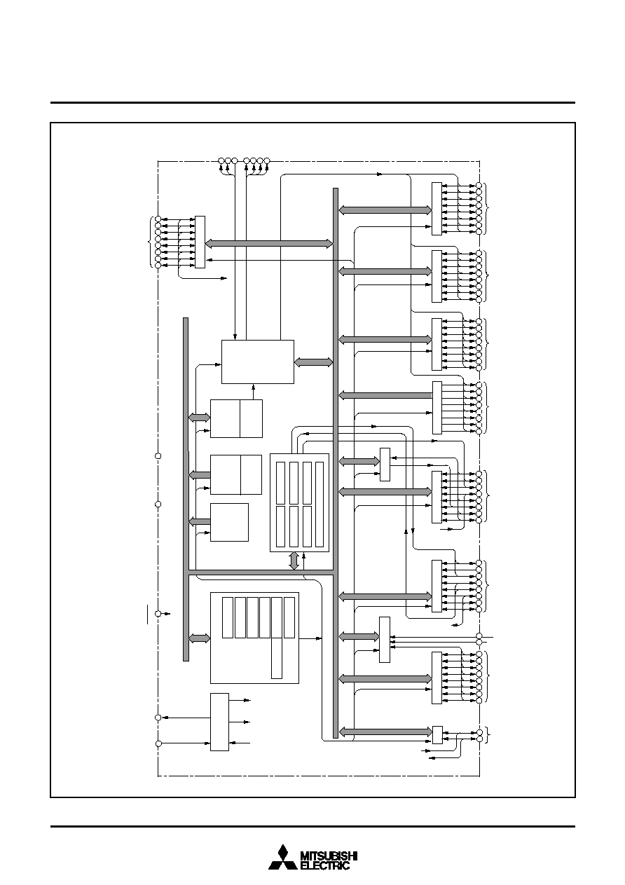
The 38C3 group is the 8-bit microcomputer based on the 740 family
core technology.
The 38C3 group has a LCD drive control circuit, a 10-channel A-D
converter, and a Serial I/O as additional functions.
The various microcomputers in the 38C3 group include variations of
internal memory size and packaging. For details, refer to the section
on part numbering.
For details on availability of microcomputers in the 38C3 group, refer
to the section on group expansion.
FEATURES
q
Basic machine-language instructions ....................................... 71
q
The minimum instruction execution time ............................. 0.5
µ
s
(at 8MHz oscillation frequency)
q
Memory size
ROM .................................................................. 4 K to 48 K bytes
RAM ................................................................. 192 to 1024 bytes
q
Programmable input/output ports ............................................. 57
q
Software pull-up/pull-down resistors
..................................................... (Ports P0≠P8 except Port P5
1
)
q
Interrupts ................................................... 16 sources, 16 vectors
(includes key input interrupt)
q
Timers ............................................................ 8-bit
!
6, 16-bit
!
1
q
A-D converter ................................................. 10-bit
!
8 channels
q
Serial I/O ....................................... 8-bit
!
1 (Clock-synchronized)
q
LCD drive control circuit
Bias ............................................................................ 1/1, 1/2, 1/3
Duty .................................................................... 1/1, 1/2, 1/3, 1/4
Common output .......................................................................... 4
Segment output ........................................................................ 32
q
2 Clock generating circuit
(connect to external ceramic resonator or quartz-crystal oscillator)
q
Power source voltage
In high-speed mode .................................................... 4.0 to 5.5 V
In middle-speed mode ................................................ 2.5 to 5.5 V
In low-speed mode ...................................................... 2.5 to 5.5 V
q
Power dissipation
In high-speed mode ........................................................... 32 mW
(at 8 MHz oscillation frequency)
In low-speed mode .............................................................. 45
µ
W
(at 32 kHz oscillation frequency, at 3 V power source voltage)
q
Operating temperature range .................................... ≠ 20 to 85∞C
APPLICATIONS
Camera, household appliances, consumer electronics, etc.
MITSUBISHI MICROCOMPUTERS
SINGLE-CHIP 8-BIT CMOS MICROCOMPUTER
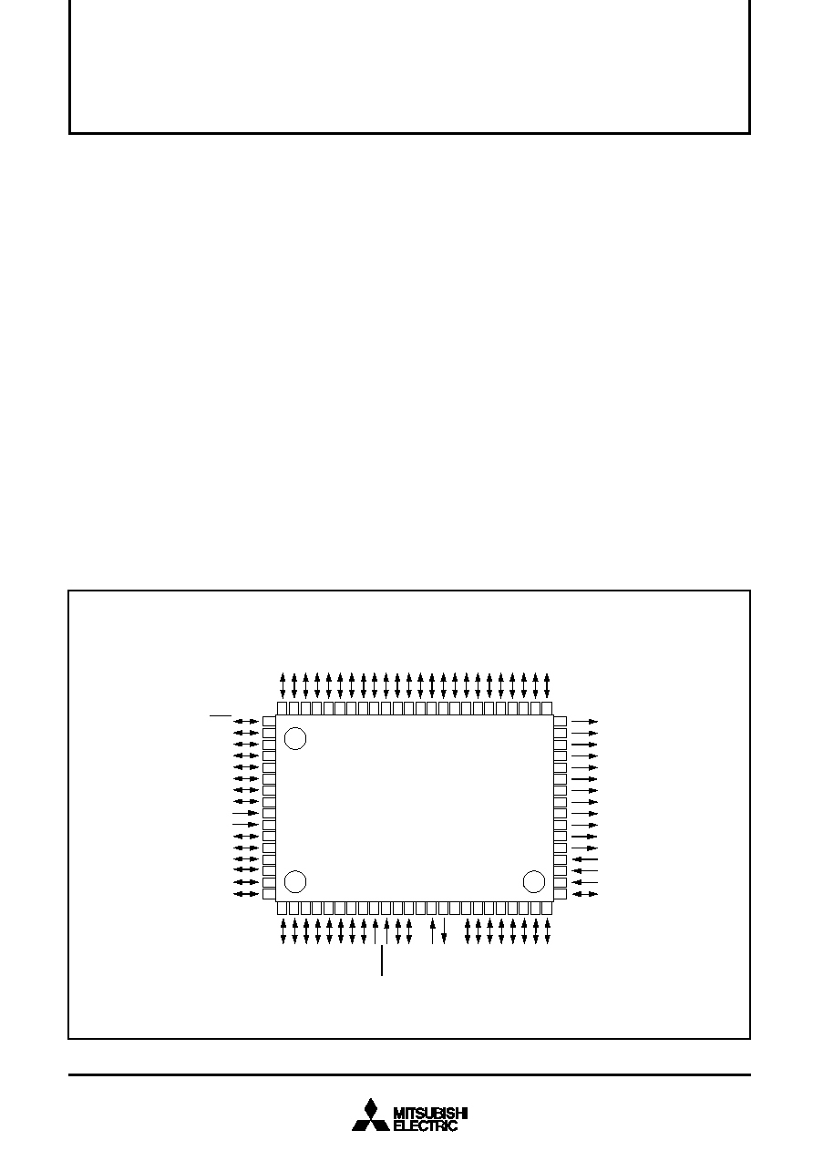
Fig. 1 M38C34M6AXXXFP pin configuration
1
25
26
27
28
29
30
31
32
33
34
35
36
37
38
39
40
64
65
66
67
68
69
70
71
72
73
74
75
76
77
78
79
80
P6
4
/AN
4
P6
5
/AN
5
P6
6
/AN
6
P6
7
/AN
7
AV
SS
V
REF
P6
0
/AN
0
P6
1
/AN
1
P6
2
/AN
2
P6
3
/AN
3
V
CC
V
SS
X
OUT
P7
0
/Xc
IN
P7
1
/Xc
OUT
X
IN
RESET
VL
1
COM
3
COM
2
COM
1
COM
0
VL
3
VL
2
P4
0
/S
CLK2
P4
2
/T3
OUT
P4
3
/
P4
4
/S
IN
P4
5
/S
OUT
P4
6
/S
CLK1
P4
7
/S
RDY
P4
1
/T1
OUT
P8
0
P8
1
P8
2
P8
3
P8
4
P8
5
P8
6
P8
7
P3
0
/SEG
24
P3
3
/SEG
27
P3
4
/SEG
28
P3
5
/SEG
29
P3
6
/SEG
30
P3
7
/SEG
31
P3
1
/SEG
25
P3
2
/SEG
26
M38C34M6AXXXFP
P5
1
P5
2
/PWM
1
P5
3
/CNTR
0
P5
4
/CNTR
1
P5
5
/INT
0
P5
6
/INT
1
P5
7
/INT
2
P5
0
/TA
OUT
P1
0
/SEG
16
P1
1
/SEG
17
P1
2
/SEG
18
P1
3
/SEG
19
P1
4
/SEG
20
P1
5
/SEG
21
P1
6
/SEG
22
P1
7
/SEG
23
P0
0
/SEG
8
P0
1
/SEG
9
P0
2
/SEG
10
P0
3
/SEG
11
P0
4
/SEG
12
P0
5
/SEG
13
P0
6
/SEG
14
P0
7
/SEG
15
P2
7
/SEG
7
P2
6
/SEG
6
P2
5
/SEG
5
P2
4
/SEG
4
P2
3
/SEG
3
P2
2
/SEG
2
P2
1
/SEG
1
P2
0
/SEG
0
63
62
61
60
59
58
57
56
55
54
53
52
51
50
49
48
47
46
45
44
43
42
41
2
3
4
5
6
7
8
9
10
11
12
13
14
15
16
17
18
19
20
21
22
23
24
3
SINGLE-CHIP 8-BIT CMOS MICROCOMPUTER
MITSUBISHI MICROCOMPUTERS
38C3 Group
∑ Apply voltage of 2.5 V to 5.5 V to V
CC
, and 0 V to V
SS
.
∑ Reference voltage input pin for A-D converter.
∑ GND input pin for A-D converter.
∑ Connect to V
SS
.
∑ Reset input pin for active "L."
∑ Input and output pins for the main clock generating circuit.
∑ Feedback resistor is built in between X
IN
pin and X
OUT
pin.
∑ Connect a ceramic resonator or a quartz-crystal oscillator between the X
IN
and X
OUT
pins to set the
oscillation frequency.
∑ If an external clock is used, connect the clock source to the X
IN
pin and leave the X
OUT
pin open.
∑ Input 0
V
L1
V
L2
V
L3
V
CC
voltage.
∑ Input 0 ≠ V
L3
voltage to LCD.
∑ LCD common output pins.
∑ COM
1
, COM
2
, and COM
3
are not used at 1/1 duty ratio.
∑ COM
2
and COM
3
are not used at 1/2 duty ratio.
∑ COM
3
is not used at 1/3 duty ratio.
∑ 8-bit I/O port.
∑ CMOS compatible input level.
∑ CMOS 3-state output structure.
∑ I/O direction register allows each port to be individually
programmed as either input or output.
∑ Pull-down control is enabled.
∑ 8-bit output port.
∑ CMOS state output.
∑ Pull-down control is enabled.
∑ 8-bit I/O port.
∑ CMOS compatible input level.
∑ CMOS 3-state output structure.
∑ I/O direction register allows each pin to be individually
programmed as either input or output.
∑ Pull-up control is enabled.
∑ LCD segment pins
∑ Serial I/O function pin
∑ Timer output pin
∑ Timer output pin
∑
output pin
∑ Serial I/O function pins
Pin
V
CC
, V
SS
V
REF
AV
SS
RESET
X
IN
X
OUT
V
L1
≠ V
L3
COM
0
≠
COM
3
P0
0
/SEG
9
≠
P0
7
/SEG
15
P1
0
/SEG
16
≠
P1
7
/SEG
23
P2
0
/SEG
0
≠
P2
7
/SEG
7
P3
0
/SEG
24
≠
P3
7
/SEG
31
P4
0
/S
CLK2
P4
1
/T
1OUT
P4
2
/T
3OUT
P4
3
/
P4
4
/S
IN
,
P4
5
/S
OUT
,
P4
6
/S
CLK1,
P4
7
/S
RDY
Name
Power source
Analog reference
voltage
Analog power
source
Reset input
Clock input
Clock output
LCD power
source
Common output
I/O port P0
I/O port P1
I/O port P2
Output port P3
I/O port P4
Function except a port function
PIN DESCRIPTION
Table 1 Pin description (1)
Function

4
SINGLE-CHIP 8-BIT CMOS MICROCOMPUTER
MITSUBISHI MICROCOMPUTERS
38C3 Group
∑ 1-bit input pin.
∑ CMOS compatible input level.
∑ 7-bit I/O port.
∑ CMOS compatible input level.
∑ CMOS 3-state output structure.
∑ I/O direction register allows each pin to be individually
programmed as either input or output.
∑ Pull-up control is enabled.
∑ 8-bit I/O port.
∑ CMOS compatible input level.
∑ CMOS 3-state output structure.
∑ I/O direction register allows each pin to be individually
programmed as either input or output.
∑ Pull-up control is enabled.
∑ 2-bit I/O port.
∑ CMOS compatible input level.
∑ CMOS 3-state output structure.
∑ I/O direction register allows each pin to be individually
programmed as either input or output.
∑ Pull-up control is enabled.
∑ 8-bit I/O port.
∑ TTL input level.
∑ CMOS 3-state output structure.
∑ I/O direction register allows each pin to be individually
programmed as either input or output.
∑ Pull-up control is enabled.
Pin
P5
1
P5
0
/TA
OUT
P5
2
/PWM
1
P5
3
/CNTR
0
,
P5
4
/CNTR
1
P5
5
/INT
0
,
P5
6
/INT
1
,
P5
7
/INT
2
P6
0
/AN
0
≠
P6
7
/AN
7
P7
0
/X
COUT,
P7
1
/X
CIN
P8
0
≠ P8
7
Table 2 Pin description (2)
Name
Input port P5
I/O port P5
I/O port P6
I/O port P7
I/O port P8
Function except a port function
∑ Timer A output pin
∑ PWM
1
output (timer output) pin
∑ External count I/O pins
∑ External interrupt input pins
∑ A-D conversion input pins
∑ Sub-clock generating circuit I/O pins
∑ Key input (Key-on wake-up) interrupt
input pins
Function
5
SINGLE-CHIP 8-BIT CMOS MICROCOMPUTER
MITSUBISHI MICROCOMPUTERS
38C3 Group
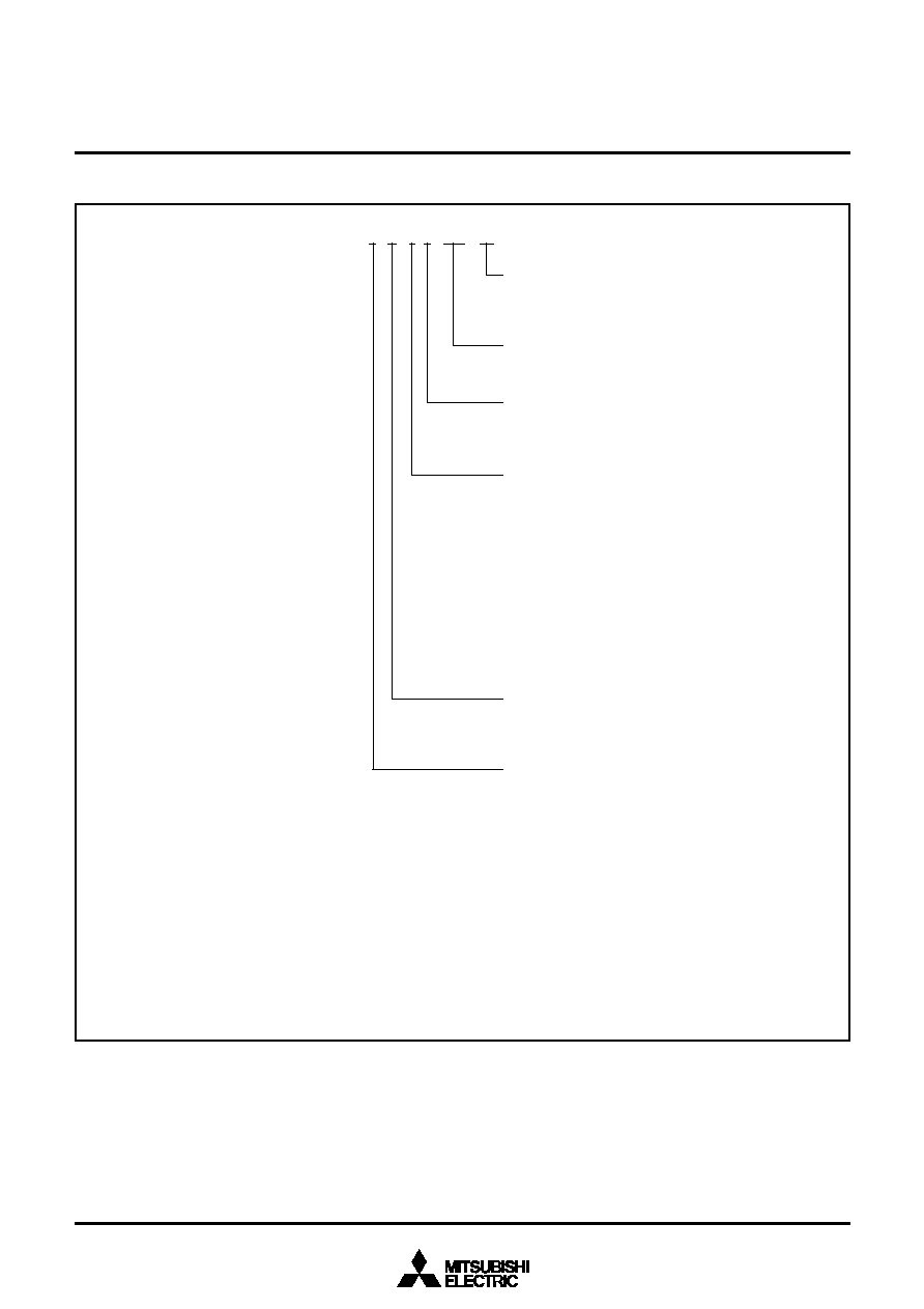
M38C3 4 M 6 A XXX
FP
Product
ROM/PROM size
1
2
3
4
5
6
7
8
: 4096 bytes
: 8192 bytes
: 12288 bytes
: 16384 bytes
: 20480 bytes
: 24576 bytes
: 28672 bytes
: 32768 bytes
The first 128 bytes and the last 2 bytes of ROM
are reserved areas ; they cannot be used.
Memory type
M
E
: Mask ROM version
: EPROM or One Time PROM version
RAM size
0
1
2
3
4
5
6
7
: 192 bytes
: 256 bytes
: 384 bytes
: 512 bytes
: 640 bytes
: 768 bytes
: 896 bytes
: 1024 bytes
Package type
FP
FS
ROM number
Omitted in some types.
A : Standard(Note)
M : M version
: 80P6N-A package
: 80D0 package
9
A
B
C
: 36864 bytes
: 40960 bytes
: 45056 bytes
: 49152 bytes
Note : Difference between standard and M version
∑ Standard :
∑ M version :
Port P5
0
/TA
OUT
pin remains set to the input mode until the direction
register is set to the output mode during reset and after
reset.
Port P5
0
/TA
OUT
pin remains set to the output mode ("L" output) until
the direction register is set to the input mode during reset
and after reset.
PART NUMBERING
Fig. 3 Part numbering