 | –≠–ª–µ–∫—Ç—Ä–æ–Ω–Ω—ã–π –∫–æ–º–ø–æ–Ω–µ–Ω—Ç: UA2B200AX | –°–∫–∞—á–∞—Ç—å:  PDF PDF  ZIP ZIP |

UA2B200AX
Contact Type Image Sensor
( 1/6 )
1.Application
This specification sheet is applied to Contact Type Image Sensor UA2B200AX.
2.
General Description
The UA2B200AX is a contact type image sensor with a valid pixel density of 200 DPI capable of
scanning an image at the rate of 250
µs/line for 200 mm width. The video signal is outputted at the
8-bit long digital value and is provided with black and white output correcting function for each
pixel.
3.
Specifications
The specifications of this contact type image sensor are shown in the table below.
Item
Specifications
Remarks
Valid scanning width
200mm
Sensor output width 207.4 mm
(Including white-basis output)
Pixel density
200dpi
Valid scanning
pixel
1574 pixel
(No. 2-1575 pixel)
Total pixel: 1632 pixels
Number of valid pixels
White-basis
output pixel
16 pixel min
(No. 1617-1632 pixel)
Minimum number of pixels at
maximum tolerance.
Storing time
250
µs/line
Feed speed
Output clock frequency
7.0MHz
Maximum 7.5 MHz
4.
Configuration
The configuration of this contact type image sensor is shown in the table below.
Item
Configuration
Remarks
Optical system
Rod lens array
Angular aperture: 20 degrees
Blue
= 470nm
(LED1,LED0)=(1,0)
Green
= 525nm
(LED1,LED0)=(0,1)
Red
= 655nm
(LED1,LED0)=(0,0)
Light source
LED light source
Infra-red
= 940nm
(LED1,LED0)=(1,1)
For sensor drive
5V
◊ (0.5A)
TBD
Blue
45mAmax.
Green
45mAmax.
Red
35mAmax.
Power supply
For LED
Infrared
50mAmax.
at LED On duty 1/4
Data output mode
8-bit width digital output
TTL output
Digital signal
processing
Black output correction by sensitiveness (pixel unit)
White output correction by sensitiveness (pixel unit)
Gain adjustment (PGA)
PGAProgrammable GainAmp.
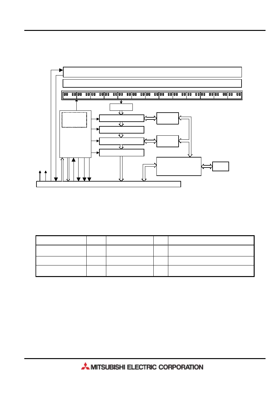
Block diagram
Fig.1
Timing diagram
Fig.2
Outline drawing
Fig.4
UA2B200AX
Contact Type Image Sensor
( 2/6 )
Fig. 1 Internal block diagram
5.
Standard Operating Conditions and Property Specifications
This contact type image sensor shall satisfy the following characteristics.
Characteristic specifications
Item
Code
Specifications
Unit
Remarks
White output
DVp
60min.
Hex
Minimum white output value after black
correction
White output uniformity
DUd
0Amax.
HEX Deviation little to the black offset
MTF
%
TBD
%
Resolution at scanning an original of 1.87
LP/mm using light source G
Note) Only black correction is made for standard shipment and no white correction.
1
864
Lod Lens Array
Line memory
2
LED Light Source
10bit ADC
Dark Correction
PGA
Offset
VDD
GND
VL
ED
L
E
D_
GNDn
LE
D
n
XSYNC
CIS_
CL
K
XSYNC_
O
U
T
XDENB
Serial Control &
Memory/Register Control
EEPROM
CN1
Line memory
White Correction
Timming
Control
CIS
Control
L
E
DCn

UA2B200AX
Contact Type Image Sensor
( 3/6 )
The measurement conditions of characteristic specifications are shown in the following.
Measurement Conditions of Property Specifications
Item
Code
Specifications
Unit
Remarks
Power voltage
VDD
+5.0
V
Red
30typ.
Green
40typ.
Blue
40typ.
LED drive current
I
LED
Infra-Red
45typ.
mA
at LED On duty 1/4
White-basis chart
0.05 - 0.09
O.D.
Storing time
Trep
250.0
µsec
Output clock rate
fCIS_CLK
7.0
MHz
Operating ambient
temperature
Ta
25
∞C
Note) 1) The definition of specification measurement item shall be as follows. The testing chart shall be placed in a
stationary state at the scanning position shown in the outline drawing (Fig. 3) for scanning.
2) Specification measurement shall all be made after black correction.
Fig. 3 LED connection equivalent circuit
VLED
CONNECTOR
LED_GND0
LED_GND1
LED_GND2
LED_GND3
Blue
Green
Red
IR
32
34
36
38
4-100Ohm(0.1W)
for LED protect

UA2B200AX
Contact Type Image Sensor
( 4/6 )
6. Timing Conditions
Item
Code
MIN
TYP
MAX
Unit
Remarks
Scanning cycle
Trep
250.0
µsec
XSYNC
XSYNC effective period
Tw(XSYNC)
500
nsec
CIS_CLK cycle
TCIS_CLK
135
143
nsec
7.0MHz typ.
CIS_CLK duty
-
45
50
55
%
Output line delay
Tldly
36
CIS_CLK
XSYNC_OUT effective width
Twxso
1
CIS_CLK
XSYNC_OUT setup time
Tsuxso
10
50
nsec
XSYNC_OUT hold time
Thdxso
50
nsec
Data output delay time
TDdly
18
19
20
CIS_CLK
DATA setup time
tDs
10
50
nsec
DATA hold time
tDh
50
nsec
LED selection setup time
Tsu(LED)
200
nsec
LED selection hold time
Thd(LED)
2
µsec
Fig. 2 Timing conditions
(Note)
1. This diagram is based on CIS_CLK. [clk] in the unit shows the number of CIS_CLKs.
2. XSYNC is valid only at falling edge.
3. LEDS,LEDEn shows Register Values of CIS signal processing unit.
XDENB
XSYNC
tDdly
(output)
DATA
1,2,3,4
1632
DATA
CIS_CLK
XSYNC_OUT
not Valid
Tw(XSYNC)
TCIS_CLK
(Input)
1
2
Tsu(LED)
TLED
(output)
twxso
XSYNC_OUT
tsuxso
thdxso
LEDn
Trep
tldly
XDENB
tDh
tDs
LEDCn
LEDS◊16CIS_CLK
LEDEn◊16CIS_CLK

UA2B200AX
Contact Type Image Sensor
( 5/6 )
b)
7.
Connector Pin Arrangement
7.1 CN1 (CIS control and signal output)
CN1 pin arrangement
Connector: SM40B-SRDS-G-TF (JST)
Pin No.
Name
Pin No.
Name
1
Data0(LSB)
2
Data1
3
Data2
4
Data3
5
GND
6
GND
7
Data4
8
Data5
9
Data6
10
Data7(MSB)
11
GND
12
GND
13
CIS_CLK
14
GND
15
XSYNC_OUT
16
XDENB
17
VDD
18
VDD
19
XSYNC
20
GND
21
XMW
22
XME
23
XUCS
24
SELBUS
25
UCK
26
GND
27
UDI
28
LEDC0
29
UDO
30
LEDC1
31
VLED
32
LED_GND0
33
LED0
34
LED_GND1
35
LED1
36
LED_GND2
37
LEDC2
38
LED_GND3
39
LEDC3
40
FG
LEDn
XSYNC
(output)
(Input)
DATA
LED0
LED1
LED2
LED3
LED0
XDENB
Image data LED 0
Invalid
Image data LED 2
Invalid
Image data LED 1
Invalid
Image data LED 3 green
Invalid
Invalid