 | –≠–ª–µ–∫—Ç—Ä–æ–Ω–Ω—ã–π –∫–æ–º–ø–æ–Ω–µ–Ω—Ç: MM1099A | –°–∫–∞—á–∞—Ç—å:  PDF PDF  ZIP ZIP |

MITSUMI
System Reset (Built-in Watch Dog Timer) MM1099
System Reset (Built-in Watch Dog Timer)
Monolithic IC MM1099
Outline
The function of this IC series MM1099 is to accurately reset systems, a generating reset signal at the time of
instantaneous supply voltage off or lowering in varied CPU and other logic system.
Further, with the watch dog timer built-in it can diagnose the operation of the system, intermittently
generating reset pulses when they operate erroneously to prevent runaway.
Features
1. Built-in watch dog timer
2. Low current consumption
130µA TYP.
3. Low operating threshold voltage
V
CC
=0.8V
4. Watch dog stop function (RCT terminal)
5. Long clock monitoring time
T
PR
(POWER ON) : T
WD
(clock monitoring)=1 : 1
6. Fewer outer components
Package
DIP-8B (MM1099AD, MM1099BD)
SOP-8C (MM1099AF, MM1099BF)
SIP-8A (MM1099AS, MM1099BS)
Applications
1. Reset circuit for microcomputers, CPU and MPU.
2. Reset circuit for logic circuitry.
3. Monitoring of microcomputer system, etc.
Pin Assignmemt
1
4
3
2
8
5
6
7
SOP-8C/DIP-8B
1
TC
2
N.C
3
CK
4
GND
5
V
CC
6
RCT
7
V
S
8
RESET
-----------------------------------------------------------
1
TC
2
N.C
3
CK
4
GND
5
V
CC
6
RCT
7
V
S
8
RESET
-----------------------------------------------------------
SIP-8A
1
3
5
7
2
4
6
8

MITSUMI
System Reset (Built-in Watch Dog Timer) MM1099
Pin Description
Pin No. Pin name
Function
1
TC
2
N.C
3
CK
4
GND
5
V
CC
6
RCT
7
V
S
8
RESET
Variable terminals T
WD
, T
WR
and T
PR
T
PR
(mS) = 5000 C
T
(µF)
The time for T
WD
, T
WR
and T
PR
to be
T
WD
(mS) = 500 C
T
(µF)
determined by the external capacitor.
T
WR
(mS) = 100 C
T
(µF)
Clock input terminal Inputs the clock from the logic system.
Ground terminal
Voltage detection MM1099A 3.2V MM1099B 4.2V
Watchdog timer stop pin Operation modes: Operation OPEN, Stop connect to GND
Detect voltage variable terminal
Reset output pin (low output)
Absolute Maximum Ratings
Item
Symbol
Rating
Units
Power supply voltage
V
CC
max.
-0.3~+10
V
CK pin input voltage
V
CK
-0.3~V
CC
+0.3 ( <
= +10)
V
V
S
pin input voltage
V
VS
-0.3~V
CC
+0.3 ( <
= +10)
V
Voltage applied to RCT pin
V
RCT
-0.3~V
CC
+0.3 ( <
= +10)
V
Voltage applied to RESET
----------------------------------------------------
pin
V
OH
-0.3~V
CC
+0.3 ( <
= +10)
V
Allowable loss
Pd
300
mW
Storage temperature
T
STG
-40~+125
∞
C
Recommended Operating Conditions
Item
Symbol
Rating
Units
Power supply voltage
V
CC
+2.2~+7.0
V
RESET
----------------------------------------------------
sync current
I
OL
0~1.0
mA
Clock monitoring time setting
T
WD
0.1~1000
mS
Clock rise and fall times
t
FC
, t
RC
<100
µS
TC pin capacitance
C
T
0.0002~2
µF
Operating temperature
T
OP
-25~+75
∞
C
MITSUMI
System Reset (Built-in Watch Dog Timer) MM1099
Electrical Characteristics (DC)
(Except where noted otherwise, MM1099A : V
CC
=3.6V, Ta=25
∞
C, MM1099B : V
CC
=5.0V)
Item
Symbol
Measurement conditions
Min. Typ. Max. Units
Consumption current
MM1099A
I
CC
During watchdog timer operation
(100) (150)
µA
MM1099B
130
195
MM1099A
V
SL
3.10 3.20 3.30
Detection voltage
MM1099B
4.05 4.20 4.35
V
MM1099A
V
SH
3.15 3.25 3.35
MM1099B
4.15 4.30 4.45
Detection voltage temperature coefficient
V
S
/ T
±0.01
%/
∞
C
Hysteresis voltage
MM1099A
V
HYS
25
50
100
mV
MM1099B
50
100
150
CK input threshold
V
TH
0.8
1.2
2
V
CK input current
I
IH
A : V
CK
=3.6V, B : V
CK
=5.0V
0
1
µA
I
IL
V
CK
=0V
-12
-6
-2
Output voltage
MM1099A
V
OH
3.0
3.4
V
(High)
MM1099B
4.0
4.5
Output voltage (Low)
V
OL
1
I
=0.5mA, V
S
=0V
0.2
0.4
V
V
OL
2
I
=1.0mA, V
S
=0V
0.3
0.5
R output sync current
I
OL
V
=1.0V, V
S
=0V
1
2
mA
C
T
charge current
I
CT
1
V
TC
=1.0V during watchdog timer operation -0.16 -0.24 -0.48
µA
I
CT
2
V
TC
=1.0V during power ON reset operation -0.16 -0.24 -0.48
µA
Minimum operating power
V
CCL
0.8
1.0
V
supply voltage to ensure RESET
---------------------------------------------------
RESET
----------------------------------------------------
RESET
----------------------------------------------------
RESET
----------------------------------------------------
V
S
=OPEN, V
CC
V
S
=OPEN, V
CC
V
SH
-V
SL
, V
CC
V
=0.4V
I
=0.1mA
RESET
----------------------------------------------------
RESET
----------------------------------------------------
I
=-1µA, V
S
=OPEN
RESET
----------------------------------------------------

MITSUMI
System Reset (Built-in Watch Dog Timer) MM1099
Electrical Characteristics (AC)
(Except where noted otherwise, MM1096A : V
CC
=3.6V, Ta=25
∞
C MM1096B : V
CC
=5.0V)
Notes :
*
1 The "monitoring time" means the time interval from the last pulse of the clock pulses for timer clear
(negative edge) to the output of the reset pulse. If the clock pulse is not input during this time interval, the
reset output will be given.
*
2 The "reset time" is no other than the reset pulse width, except when resetting the POWER ON.
*
3 The "reset hold time" is the time interval from the time point when V
CC
exceeds the detect (V
SH
) at the time
of Power On Reset (Power variation reset) to the reset release (RESET
-------------------------------------------------
output "HIGH").
*
4 The "output delay time" means the time interval from when the supply voltage comes lower than the
detect voltage (V
SL
) to when comes the reset state (RESET
-------------------------------------------------
output "Low").
*
5 The voltage range is 10 to 90% when measuring the output rise and fall times.
*
6 By varying the capacitance of C
T
, we can vary the watch dog timer monitoring time (T
WD
), the reset time at
the time of the watch dog timer (T
WR
), and the reset hold time at the time of power source rise (T
PR
). The
variable time can be expressed by the following formulas:
T
PR
(mS)
.
=. 5000 C
T
(µF)
T
WD
(mS)
.
=. 5000 C
T
(µF)
T
WR
(mS)
.
=. 100 C
T
(µF)
Example : When CT=0.02µF
T
PR
.
=. 100mS
T
WD
.
=. 100mS
T
WR
.
=. 2mS
Item
Symbol Measurement
conditions
Min.
Typ.
Max.
Units
MM1099A
8
V
CC
input
T
PI
µS
pulse width
MM1099B
8
CK input pulse width
T
CKW
3
µS
CK input cycle
T
CK
20
µS
Watchdog timer
monitoring time
*
1
T
WD
C
T
=0.02µF
50
100
150
mS
Reset time for
watchdog timer
*
2
T
WR
C
T
=0.02µF
1
2
3
mS
Reset hold time for
power supply rise
*
3
T
PR
50
100
150
mS
Output delay time from V
CC
*
4
T
PD
RESET
----------------------------------------------------------------------
pin, R
L
=10k
, C
L
=20pF
2
10
µS
Output rise time
*
5
t
R
RESET
----------------------------------------------------------------------
pin, R
L
=10k
, C
L
=20pF
2.0
4.0
µS
Output fall time
*
5
t
F
RESET
----------------------------------------------------------------------
pin, R
L
=10k
, C
L
=20pF
0.2
1.0
µS
V
CC
3.6V
2.8V
V
CC
5.0V
4.0V
C
T
=0.02µF, V
CC
CK
or
MITSUMI
System Reset (Built-in Watch Dog Timer) MM1099
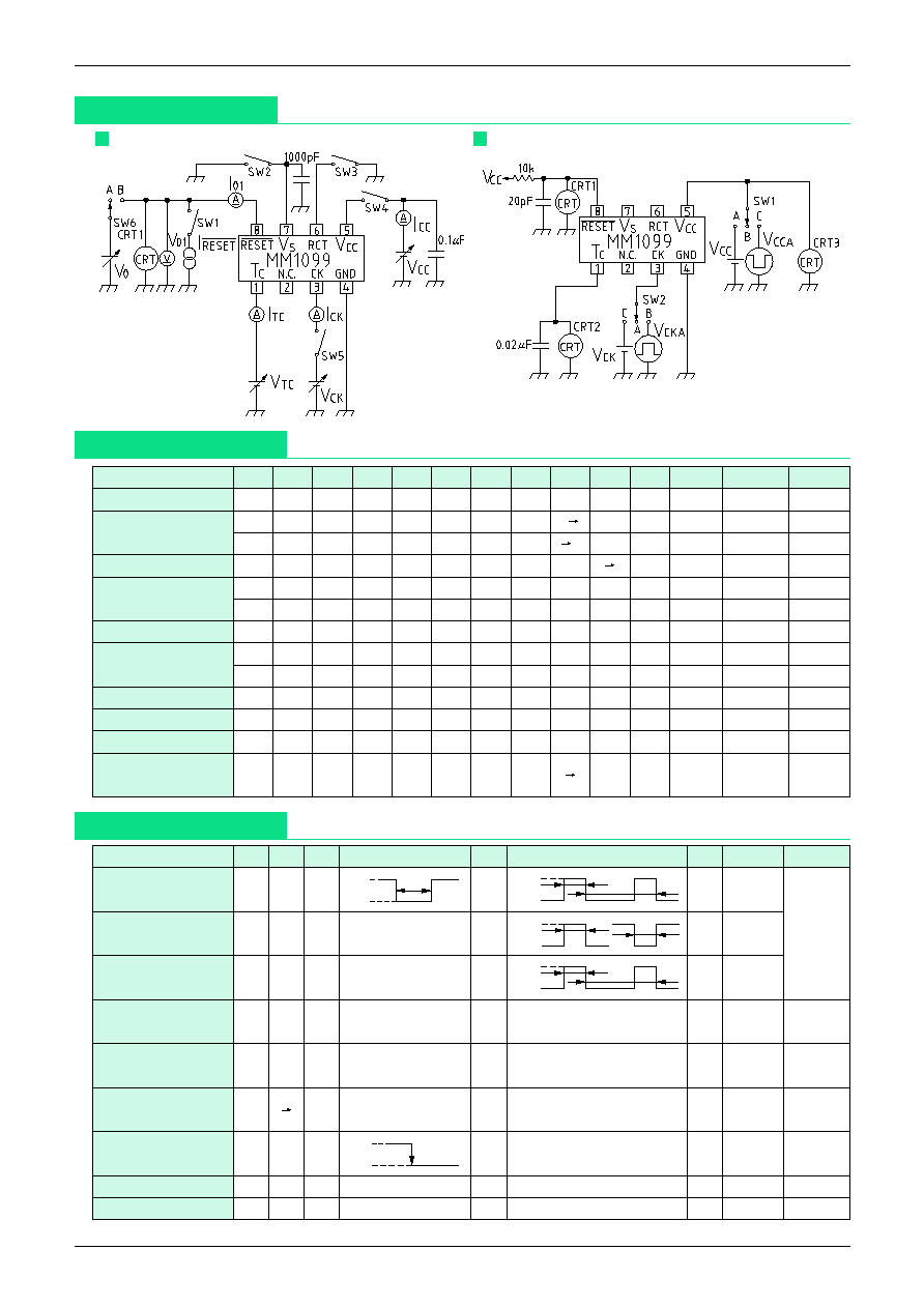
Measuring Circuits
Measuring Circuit 1 (DC)
Measuring Circuit 2 (AC)
Measuring Circuit 1
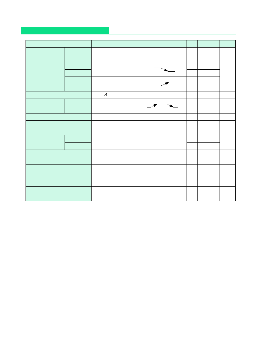
SW & Power Supply Table
Measuring Circuit 2
SW & Power Supply Table
Item
Symbol SW1 SW2 SW3 SW4 SW5 SW6 SW7
V
CC
V
CK
V
CT
I
VM, IM
Notes
Consumption current
I
CC
OFF
OFF
OFF
ON
ON
ON
A
3.6V
3.6V
0V
-
I
CC
Detection voltage
V
SL
OFF
OFF
ON
ON
ON
ON
A
3.6V 3V
0V
2V
-
V
O
1, CRT1
V
SH
OFF
OFF
ON
ON
ON
ON
A
3V 3.6V
0V
2V
-
V
O
1, CRT1
CK input threshold
V
TH
OFF
OFF
OFF
ON
ON
ON
A
3.6V 0V 3V
1V
-
I
CK
, V
CK
CK input current
I
IH
OFF
OFF
OFF
ON
ON
ON
A
3.6V
3.6V
0V
-
I
CK
I
IL
OFF
OFF
OFF
ON
ON
ON
A
3.6V
0V
0V
-
I
CK
Output voltage (High)
V
OH
ON
OFF
ON
ON
ON
ON
A
3.6V
3.6V
2V
-1µA
V
O
1
Output voltage (Low)
V
OL
1
ON
ON
ON
ON
ON
ON
A
3.6V
3.6V
2V
0.5mA
V
O
1
V
OL
2
ON
ON
ON
ON
ON
ON
A
3.6V
3.6V
2V
1.0mA
V
O
1
Output sink current
I
OL
1
OFF
ON
ON
ON
ON
ON
B
3.6V
3.6V
2V
-
I
O
1
V
O
=1V
C
T
charge current 1
I
TC
1
OFF
OFF
OFF
ON
ON
OFF
A
3.6V
-
1V
-
I
TC
C
T
charge current 2
I
TC
2
OFF
OFF
OFF
ON
ON
OFF
A
3.6V
-
IV
-
I
TC
Minimum operating power
supply voltage to ensure RESET
------------------------------------------------------
V
CCL
ON
OFF
ON
ON
ON
ON
A
0V 2V
0V
0V
-
V
O1
, V
CC
RESET
-----------------------------------------------
Item
Symbol SW1 SW2
V
CCA
V
CC
V
CKA
V
CK
CRT
Notes
V
CC
input pulse width
T
P
1
C
B
-
-
CRT1
T1=8µS
CRT2
CK input pulse width T
CKW
A
B
-
3.6V
-
CRT1
T2=3µS
CRT2
CK input cycle
T
CK
A
B
-
3.6V
-
CRT1
T3=20µS
CRT2
Watchdog timer
T
WD
A
A
-
3.6V
-
3.6V
CRT1
monitoring time
CRT2
Reset time
T
WR
A
A
-
3.6V
-
3.6V
CRT1
for watchdog timer
CRT2
Reset hold time for
T
PR
B A
A
-
3.6V
-
3.6V
CRT1
power supply rise
CRT2
Output delay time
from V
CC
T
PD
C
A
-
-
0V
CRT1
Output rise time
T
R
A
A
-
3.6V
-
3.6V
CRT1
Output fall time
T
F
A
A
-
3.6V
-
3.6V
CRT1
3.6V
2.8V
T1
1.4V
0V
T2
T3
1.4V
0V
T2
T2
or
1.4V
0V
3.6V
0V
T2
T3