 | ÐлекÑÑоннÑй компоненÑ: MM1100 | СкаÑаÑÑ:  PDF PDF  ZIP ZIP |
Äîêóìåíòàöèÿ è îïèñàíèÿ www.docs.chipfind.ru
MITSUMI
Compander IC MM1100
MITSUMI
Compander IC
Monolithic IC MM1100
Outline
This IC was developed for use in mobile communication equipment. It is a compander IC incorporating
compressor/expander circuits for a significant noise reduction effect without complicated external circuitry.
On the transmission side, the dynamic range of audio signals is compressed by the compressor circuit; on the
receiving side, the expander expands the signals. As a result the dynamic range over the transmission
channel is reduced logarithmically by one-half.
Features
1. Can be driven at low voltages (down to 2.4V)
2. Compression and expansion circuits enable suppression of unwanted radio waves
3. Consumption current 2.8mA typ.
Package
SOP-14B (MM1100XF)
Applications
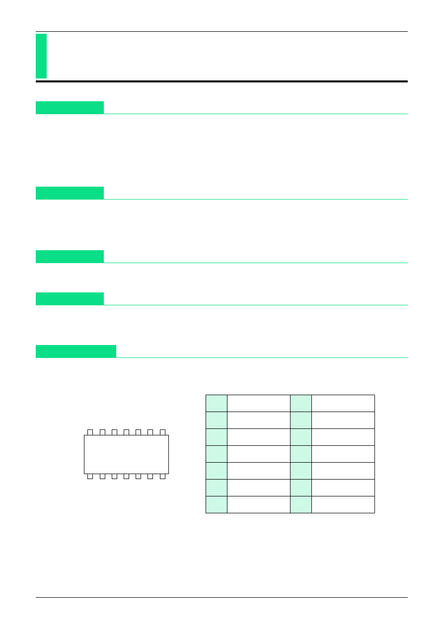
Pin Assignment
1. Cordless telephones
2. Various mobile communication devices
SOP-14B
1
3
6
2
4
5
7
14
11
9
13 12
10
8
1
E.GIN
8
C.OUT
2
E.RIN
9
C.GIN
3
E.RECT
10
C.RIN
4
E.OUT
11
C.RECT
5
E.REF
12
C.IN
6
C.REF
13
C.NF
7
GND
14
V
CC
MITSUMI
Compander IC MM1100
MITSUMI
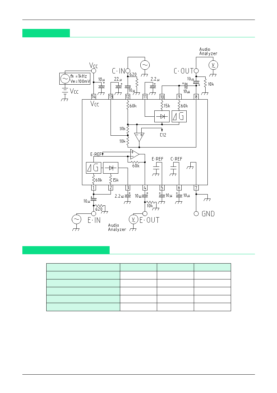
Block Diagram
Absolute Maximum Ratings
(Ta=25
°
C)
Item
Symbol
Ratings
Units
Storage temperature
T
STG
-40~+125
°
C
Operating temperature
T
OPR
-10~+70
°
C
Power supply voltage
V
CC
max.
-0.3~+8
V
Allowable loss
Pd
350
mW
Operating voltage
V
OP
+2.4~+7
V
MITSUMI
Compander IC MM1100
MITSUMI
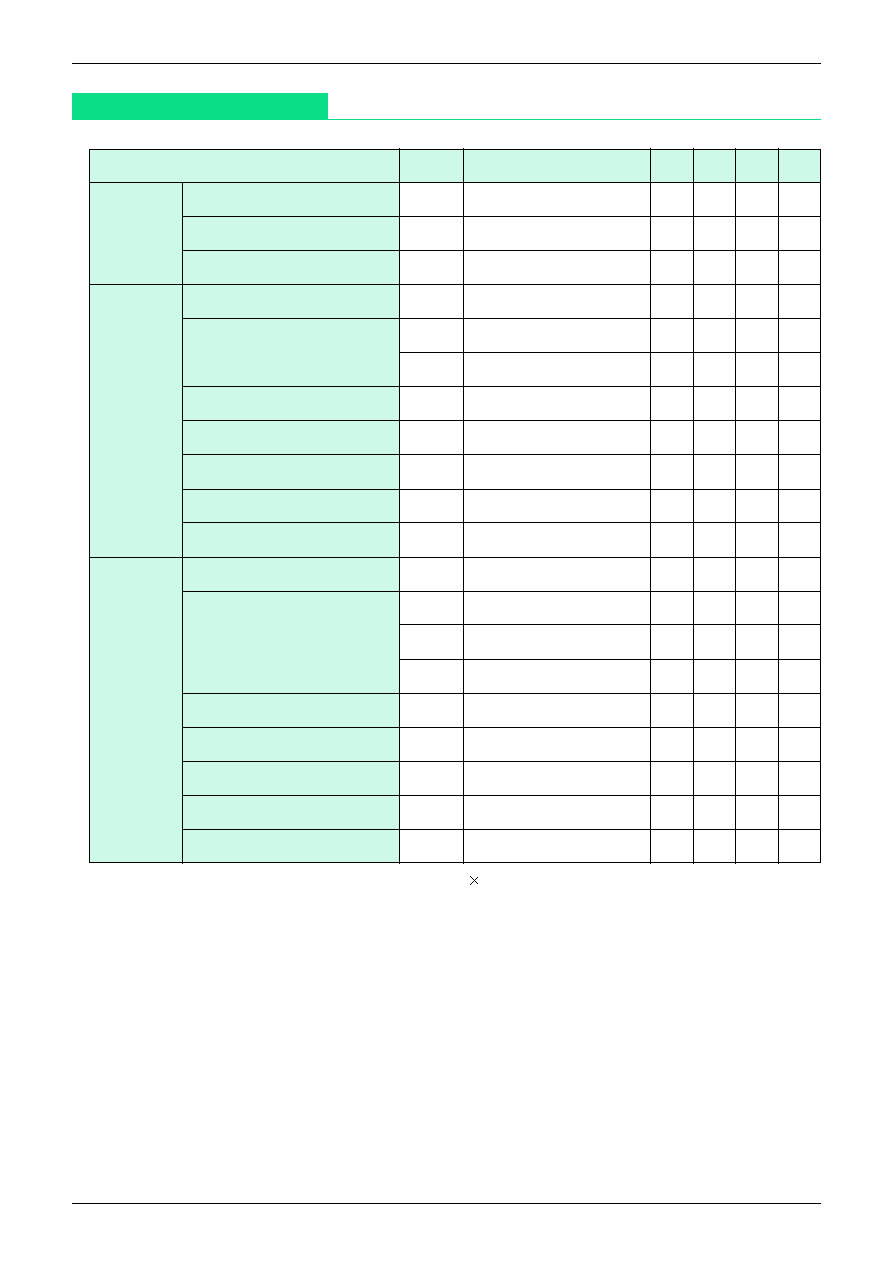
Electrical Characteristics
(Except where noted otherwise, Ta=25
°
C, Vcc=3V, f
IN
=1kHz, VR=0mVrms)
Item
Symbol
Measurement conditions
Min. Typ. Max. Units
Consumption current
I
CC
No signal
1.8
2.8
3.8
mA
Compressor reference voltage
Vrefc
6PIN DC voltage
1.3
1.4
1.5
V
Expander reference voltage
Vrefc
5PIN DC voltage
1.3
1.4
1.5
V
Input reference level
Vinc
V
OC
=300mVrms, V
IN
=0dB
100
120
145 mVrms
Gain error difference
*
Gec1
V
IN
=-20dB
-0.5
0
0.5
dB
Gec2
V
IN
=-40dB
-1.0
0
1.0
dB
Distortion
THDC
V
IN
=0dB
0.3
1.0
%
Output noise voltage
Vnc
No signal (CCITT)
2.5
5.0
mVrms
Limit voltage
Vlimc
THD=10%
1.20
1.40
1.60
V
P-P
Crosstalk
CT
C
EXPV
IN
=0dB
-45
-35
dB
Ripple rejection ratio
RR
C
V
R
=100mVrms, f
R
=1kHz
-20
-12
dB
Input reference level
Vine
Voe=300mVrms, V
IN
=0dB
310
375
450 mVrms
Gee1
V
IN
=-10dB
-0.5
0
0.5
dB
Gain error difference
*
Gee2
V
IN
=-20dB
-1.0
0
1.0
dB
Gee3
V
IN
=-30dB
-1.5
0
1.5
dB
Distortion
THDe
V
IN
=0dB
0.15
1.0
%
Maximum output voltage
Ve max.
THD=10%
700
900
mVrms
Output noise voltage
Vne
No signal (CCITT)
20
40
uVrms
Crosstalk
CTe
COMPV
IN
=0dB
-75
-60
dB
Ripple rejection ratio
RRe
V
R
=100mVrms, f
R
=1kHz
-60
-50
dB
Compressor
unit
Expander
unit
*
Gain error difference = (V
OUT
(dBv) + 10.46dB) -V
IN
(dB) G (dB)
G : COMP=0.5, EXP=2
MITSUMI
Compander IC MM1100
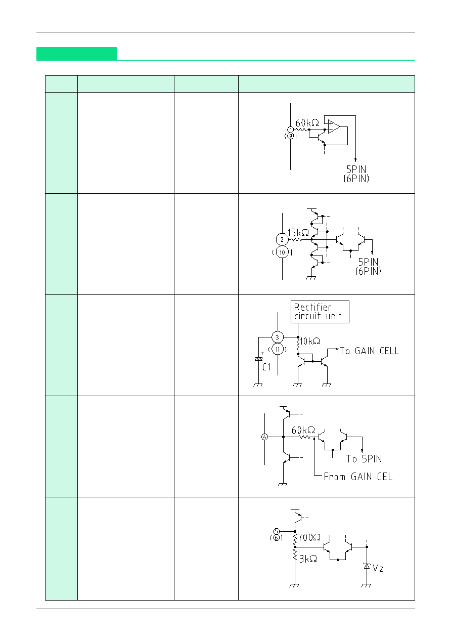
Pin no.
Function
Pin voltage (typ.)
Internal equivalent circuit
MITSUMI
Pin Description
1
Input pin E
1.4V
9
Feedback signal input pin
1.4V
2
Rectifier input pin E
1.4V
10
Rectifier input pin C
1.4V
3
Rectifier pin E
0.7V
11
Rectifier pin C
0.7V
5
Reference voltage pin E
1.4V
6
Reference voltage pin C
1.4V
4
Output pin E
1.4V
The rectifier is a full-wave
rectifier. The response
characteristics (attack time,
release time) are determined
by the time constant of the
external capacitor C1 and the
internal resistance (10k
)
MITSUMI
Compander IC MM1100
MITSUMI
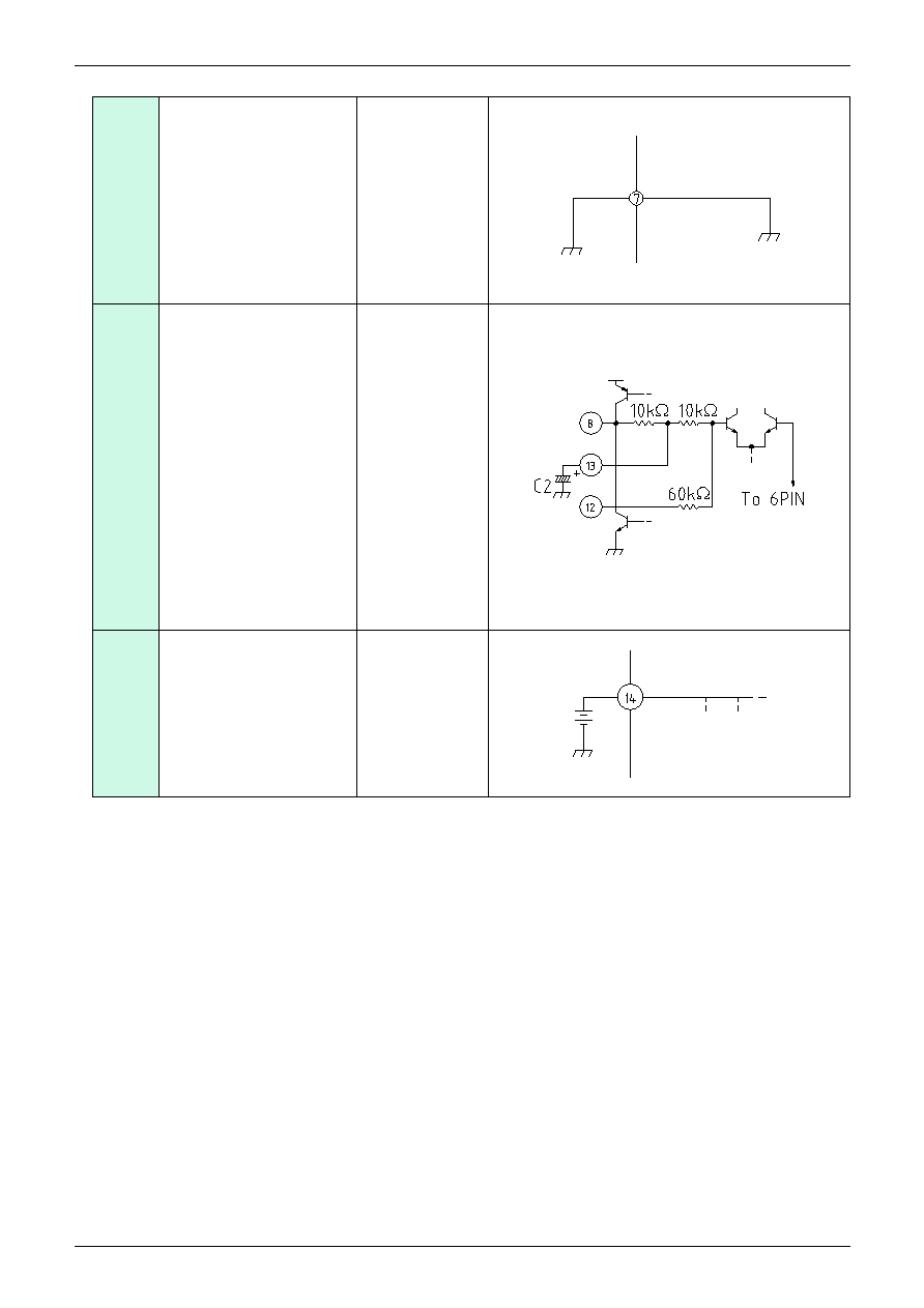
7
GND pin
0V
8
Output pin C
1.4V
12
Input pin E
1.4V
13
AC signal cut pin
1.4V
14
V
CC
pin
3.0V
The compressor amp must
have a DC gain of unity and AC
gain of infinity. In order to
satisfy this requirement, a
capacitor C2 is connected to
pin 13 to remove AC
components. The cutoff
frequency is determined by the
product with the internal
resistance (10k
)