
MITSUMI
System Reset (with battery back-up) MM1134
System Reset (with battery back-up)
Monolithic IC MM1134
Outline
These ICs protect S-RAM data in back-up mode (CS signal makes R-SAM CE pin low and CE
-------------------------------------------
pin high) when
power supply voltage goes below a certain set voltage (detection voltage 3.5V, 4.2V typ.). Further, it switches
from main power supply to battery back-up when power supply voltage drops. Conversely, when power
supply rises, it first switches the S-RAM from battery back-up to main power supply (switching voltage 3.3V
typ.), then from back-up mode to normal mode (CS signal makes S-RAM CE pin high and CE pin low). These
signal processes provide reliable protection against data damage.
Features
1 Power supply switching circuit (switching between main power supply and battery)
2 CS control for S-RAM (normal mode : S-RAM can be accessed, back-up mode: S-RAM can not be
accessed low current consumption mode)
3 With CS signal gate circuit
Characteristics
1. Battery back-up
1. Low IC current consumption (loss current)
0.3µA typ.
2. Drop voltage inside IC (input/output voltage difference)
I
O
=100µA
0.3V typ.
3. Reverse current (reverse leak current)
0.1µA max.
2. Normal operation
1. Drop voltage inside IC (input/output voltage difference)
I
O
=50µA
0.2V typ.
2. Output voltage V
CC
=5V
I
O
=50mA
4.8V typ.
3. Battery-V
CC
switching voltage
3.3V typ.
4. Detection voltage (CS, CS
-
--------------------------------------------------------
, reset output)
A : 3.5V typ.
B : 4.2V typ.

MITSUMI
System Reset (with battery back-up) MM1134
Package
SOP-8C (MM1134 F)
*
contains detection voltage rank.
Applications
1. Memory cards (S-RAM cards)
2. PCs, word processors
3. Fax machines, photocopiers, other office equipment
4. Sequence controllers, other FA equipment
5. Video games and other equipment with S-RAMs
Pin no.
Pin name
1
GND
2
RESET
3
CS
4
V
BATT
5
CS
6
V
OUT
7
Y
8
V
CC
Pin Assignment
1
4
3
2
8
5
6
7
SOP-8C
(TOP VIEW)
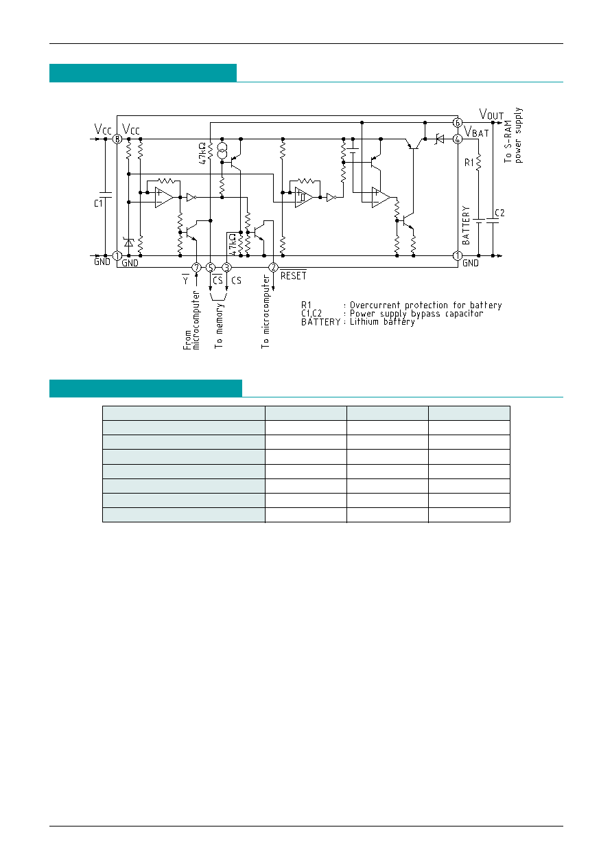
Block Diagram
MITSUMI
System Reset (with battery back-up) MM1134
Equivalent Circuit Diagram
Absolute Maximum Ratings
(Ta=25
∞
C)
Item
Symbol
Rating
Units
Storage temperature
T
STG
-40~+125
∞
C
Operating temperature
T
OPR
-20~+75
∞
C
Power supply voltage
V
CC
max.
-0.3~7
V
Operating voltage
V
CCOP
-0.3~7
V
Allowable loss
Pd
300
mW
Output current
I
O
1
80
mA
Output current
I
O
2
200
µA
Note : I
O
1 expresses V
CC
output current value, and I
O
2 expresses V
BATT
output current value.

MITSUMI
System Reset (with battery back-up) MM1134
Electrical Characteristics
Typical model: MM1134B(Except where noted otherwise, Ta=25∞C, V
CC
=V
RS
=5V, R
RS
=10k
)
Note : When input pulse rise and fall time is less than 6Nsec.
Item
Symbol
Measuring
Measurement conditions
Min. Typ. Max. Units
circuit
Consumption current
I
CC
1
V
CC
=5V, V
BATT
=3V, I
O
1=0mA
1.4
2.2
mA
I/O voltage difference 1
V
SAT
1
1
V
CC
=5V, V
BATT
=3V, I
O
1=1mA
0.03
0.05
V
Output voltage 1
V
O
1
1
V
CC
=5V, V
BATT
=3V, I
O
1=1mA
4.95
4.97
V
Output voltage 2
V
O
2
1
V
CC
=5V, V
BATT
=3V, I
O
1=15mA
4.75
4.90
V
Output voltage 3
V
O
3
1
V
CC
=5V, V
BATT
=3V, I
O
1=50mA
4.70
4.80
V
Detection voltage
V
S
1
V
CC
=H L
4.00
4.20
4.40
V
Hysteresis voltage
V
S
1
V
CC
=L H
50
100
200
mV
Reset output voltage L
V
RSL
1
V
CC
=3.7V
0.2
0.4
V
Reset leakage current H
I
RSH
1
V
CC
=5V, V
RS
=7.0V
±0.01 ±0.1
µA
Reset operation limit voltage
V
OPL
1
V
RSL
0.4V, V
CC
=H L
0.8
1.2
V
CS output voltage L
V
CSL
1
V
CC
=3.7V, V
BATT
=3V, I
CS
=1µA
0.1
V
CS output voltage H
V
CSH
1
V
CC
=5V, V
BATT
=3V, I
CS
=-1µA
4.90
V
CS output voltage L
V
CSL
1
V
CC
=5V, V
BATT
=3V, I
CS
=1µA, V
Y
=0V
0.2
V
CS output voltage H
V
CSH
1
V
CC
=3.7V, V
BATT
=3V, I
CS
=-1µA, V
Y
=0V
V
O
-0.1
V
V
CC
=5V, V
BATT
=3V, I
CS
=-1µA, V
Y
=5V
Detection voltage temperature characteristic
V
S
/ T
1
±0.05 %/
∞
C
Power supply switching voltage
V
B
1
V
CC
=H L
3.15
3.30
3.45
V
Hysteresis voltage
V
B
1
V
CC
=L H
50
100
200
mV
Switching voltage temperature characteristic V
B
/ T
1
±0.05 %/
∞
C
Loss current
I
BL
1
V
CC
=0V, V
BATT
=3V, I
O
2=0µA
0.3
0.5
µA
I/O voltage difference 2
Vsat2
1
V
CC
=0V, V
BATT
=3V, I
O
2=1µA
0.2
0.3
V
Output voltage 4
V
O
4
1
V
CC
=0V, V
BATT
=3V, I
O
2=1µA
2.7
2.8
V
Output voltage 5
V
O
5
1
V
CC
=0V, V
BATT
=3V, I
O
2=100µA
2.6
2.7
V
Reverse current
I
OREV
1
V
CC
=5V, V
BATT
=0V
0.1
µA
Y pin Lo level current
I
YLO
1
V
CC
=5V, V
BATT
=3V, V
Y
=0V
150
400
µA
Y pin
tp
LH
2
V
Y
=L H, C
L
=15pF
*
8
20
ns
Pin transmission delay time
tp
HL
2
V
Y
=H L, C
L
=15pF
*
8
20
ns
Reference voltage (typical)
V
REF
1.25
V
