MITSUMI
6-Input 1-Output Video Switch MM1140
Absolute Maximum Ratings
(Ta=25�C)
Item
Symbol
Ratings
Units
Storage temperature
T
STG
-40~+125
�C
Operating temperature
T
OPR
-20~+75
�C
Power supply voltage
V
CC
15
V
Allowable loss
Pd
350
mW
Electrical Characteristics
(Except where noted otherwise, Ta=25�C, V
CC
=5.0V)
Item
Symbol
Measurement conditions
Min. Typ. Max. Units
Operating power supply voltage range
V
CC
4.75
5.0
13.0
V
Consumption current
Id
Refer to Measuring Circuit
9.0
13.0
mA
Voltage gain
G
V
Refer to Measuring Circuit
-0.5
0
+0.5
dB
Frequency characteristic
F
C
Refer to Measuring Circuit
-1
0
+1
dB
Differential gain
DG
Refer to Measuring Circuit
0
�3
%
Differential phase
DP
Refer to Measuring Circuit
0
�3
deg
Crosstalk
C
T
Refer to Measuring Circuit
-70
-60
dB
Total harmonic distortion
THD
Refer to Measuring Circuit
0.01
0.3
%
Output offset voltage
Voff
Refer to Measuring Circuit
�30
mV
Switch input voltage
H
V
IH
Refer to Measuring Circuit
2.1
V
L
V
IL
Refer to Measuring Circuit
0.7
V
Input impedance
Ri
15
k
Output impedance
Ro
25

MITSUMI
6-Input 1-Output Video Switch MM1140
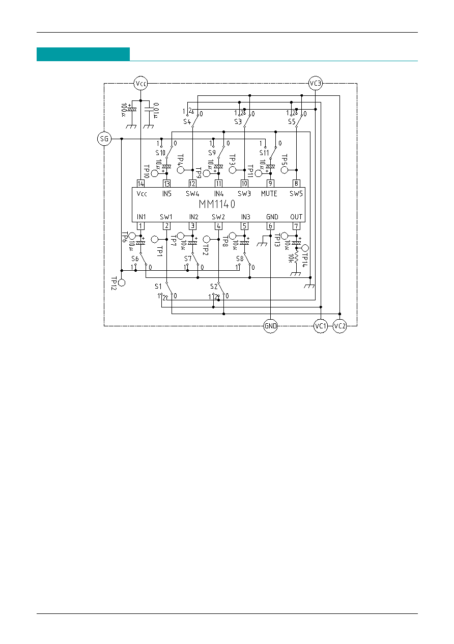
Measuring Procedures
(Except where noted otherwise, V
CC
=5.0V, VC1=V
CC
, VC2=0V)
Item
Symbol
Switch
Measuring Procedure
state
Consumption current
Id
1
Voltage gain
G
V
2
Frequency
F
C
2
characteristic
Differential gain
DG
2
Differential phase
DP
2
Total harmonic
THD
2
distortion
Output offset voltage
Voff
3
Crosstalk
C
T
9
H
V
IH
1
Switch 1
4
input voltage
L
V
IL
1
H
V
IH
2
Switch 2
5
input voltage
L
V
IL
2
H
V
IH
3
Switch 3
6
input voltage
L
V
IL
3
H
V
IH
4
Switch 4
7
input voltage
L
V
IL
4
H
V
IH
5
Switch 5
8
input voltage
L
V
IL
5
Connect a DC ammeter to the V
CC
pin and measure. V
CC
is 5V and
the ammeter is shorted for use in subsequent measurements.
Input a 2.0V
P-P
, 100kHz sine wave to SG, and obtain G
V
from the
following formula given TP12 voltage as V1 and TP14 voltage as V2.
G
V
=20LOG (V2/V1) dB
For the above G
V
measurement, given TP14 voltage for 10MHz as
V3, F
C
is obtained from the following formula.
F
C
=20LOG (V3/V2) dB
Input a 2.0V
P-P
staircase wave to SG, and measure differential gain at TP14.
APL=10~90%
Proceed as for DG, and measure differential phase.
Input a 2.5V
P-P
, 1kHz sine wave to SG, connect a distortion meter to
TP14 and measure.
Measure the DC voltage difference of each switch status at TP13.
Assume VC1=2.1V, VC2=0.7V.
Input a 2.0V
P-P
, 4.43MHz sine wave to SG, and given TP12 voltage as V4
and TP14 voltage as V5, C
T
is obtained from the following formula.
C
T
=20LOG (V5/V4) dB
Impress different optional DC voltages on TP6 and TP7. Gradually
raise from VC3=0V. TP1 voltage when TP7 voltage is output on TP13
is V
IH
1. Gradually lower from VC3=V
CC
. TP1 voltage when TP6
voltage is output on TP13 is V
IL
1.
Impress different optional DC voltages on TP6 and TP8. Gradually
raise from VC3=0V. TP2 voltage when TP8 voltage is output on TP13
is V
IH
2. Gradually lower from VC3=V
CC
. TP2 voltage when TP6
voltage is output on TP13 is V
IL
2.
Impress different optional DC voltages on TP6 and TP9. Gradually
raise from VC3=0V. TP3 voltage when TP9 voltage is output on TP13
is V
IH
3. Gradually lower from VC3=V
CC
. TP3 voltage when TP6
voltage is output on TP13 is V
IL
3.
Impress different optional DC voltages on TP9 and TP10. Gradually
raise from VC3=0V. TP4 voltage when TP10 voltage is output on
TP13 is V
IH
4. Gradually lower from VC3=V
CC
. TP4 voltage when TP9
voltage is output on TP13 is V
IL
4.
Impress different optional DC voltages on TP6 and TP11. Gradually
raise from VC3=0V. TP5 voltage when TP11 voltage is output on
TP13 is V
IH
5. Gradually lower from VC3=V
CC
. TP5 voltage when TP6
voltage is output on TP13 is V
IL
5.