MITSUMI
Superimpose MM1166
Superimpose
Monolithic IC MM1166
Outline
This is a superimpose IC that supports S-VHS, with 1 circuit for Y signals and 1 circuit for C signals, with
built-in character level and border level. The level is suppressed to eliminate the problem of spike noise
generated when switching between input video signal and character signal.
Features
1. Supports S-VHS
2. Built-in character and border levels
3. Frequency response
Y : 10MHz
C : 5MHz
4. Input/output signal
1V
P-P
5. Operating power supply voltage range
4.5~5.5V
Package
SOP-8C (MM1166XF)
Applications
1. TV
2. VCR
3. VCR with camera
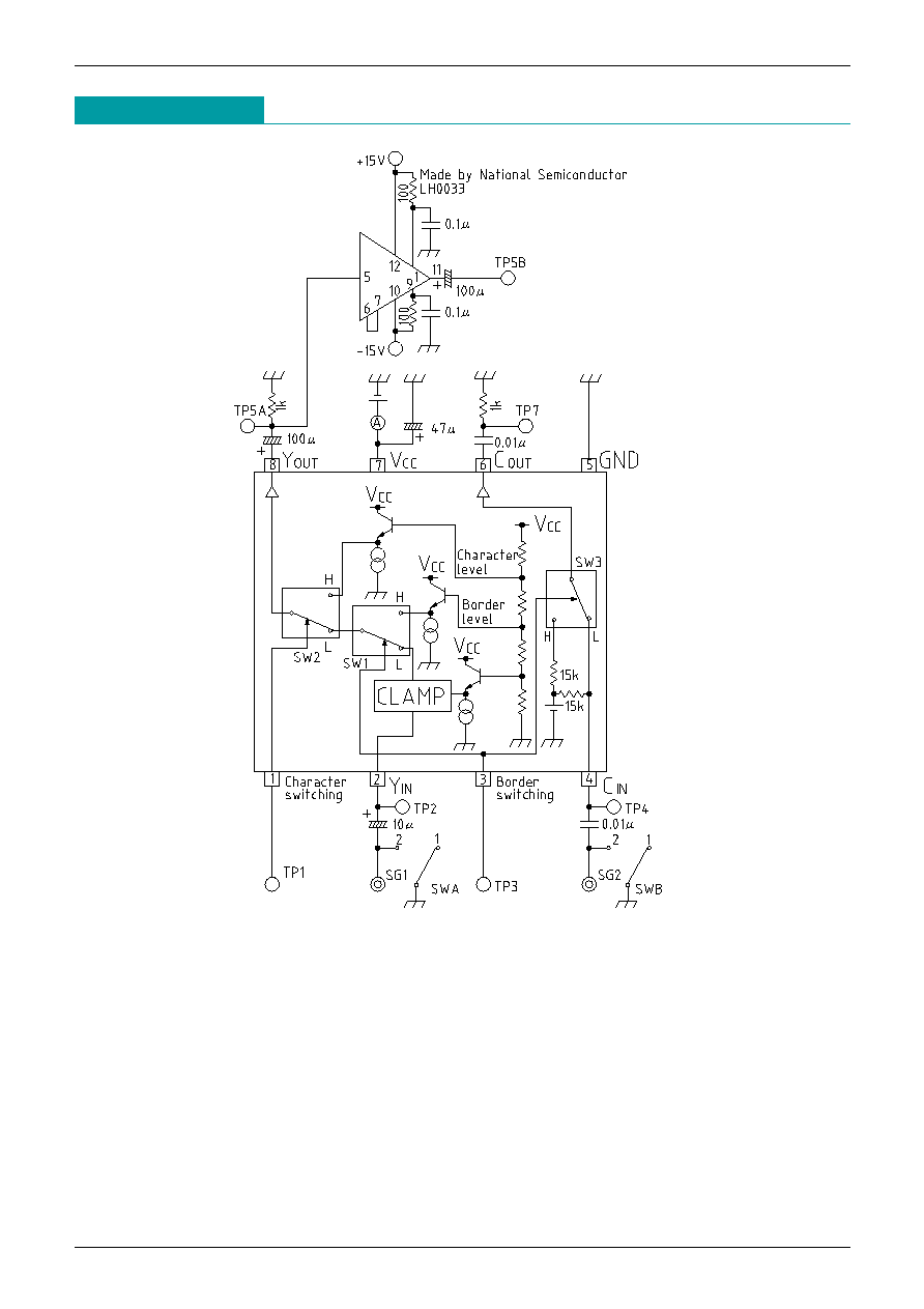
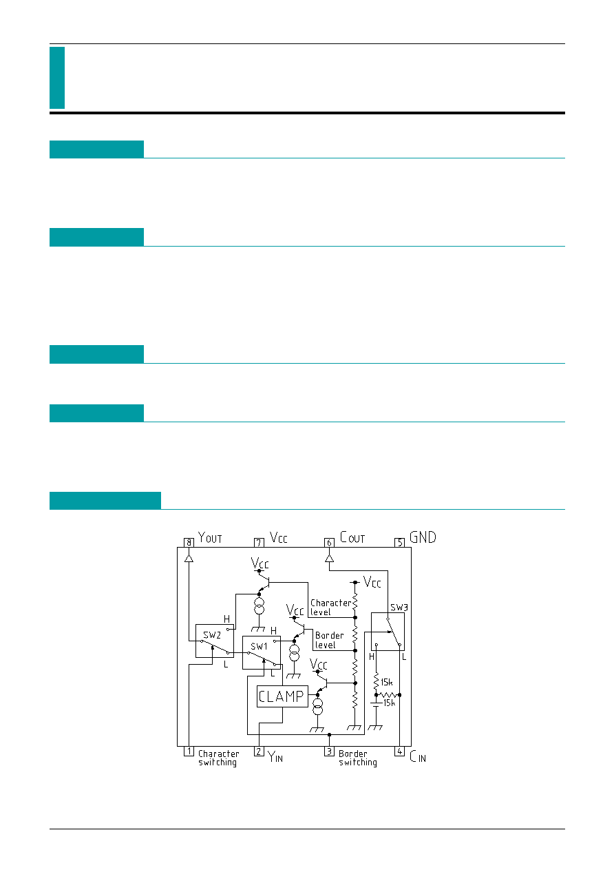
Block Diagram
MITSUMI
Superimpose MM1166
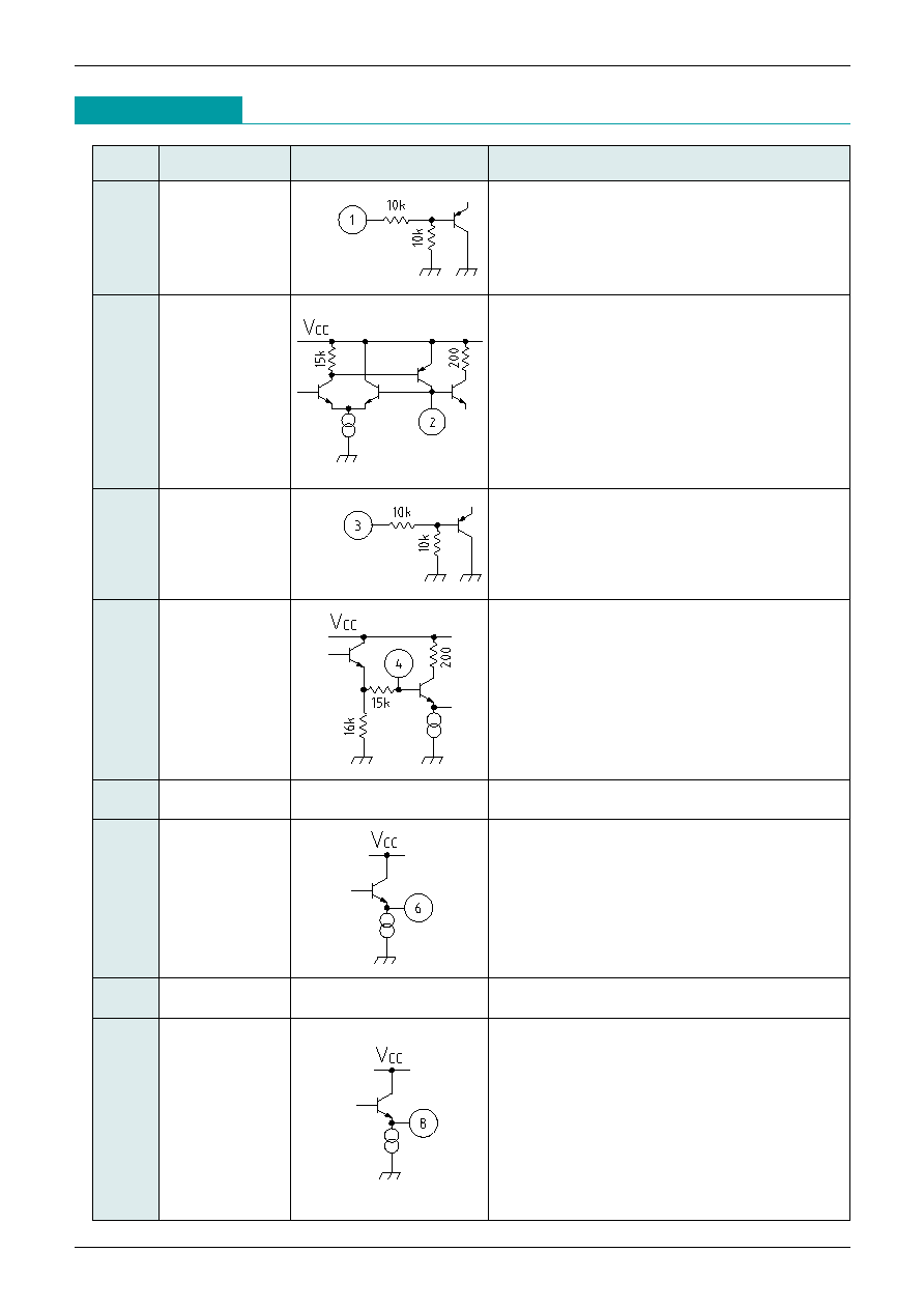
Pin Description
Pin no.
Pin name
Internal equivalent circuit diagram
Pin Description
1
Character switching
2
Y
IN
3
Border switching
4
C
IN
5
GND
6
C
OUT
Input pin for pulse that switches input signal
and character signal
High : character level output
Luminance signal input pin
Input pin for pulse that switches input signal
and border signal
High : border level output
Chroma signal input pin
GND
Chroma signal output pin
7
V
CC
8
Y
OUT
Luminance signal output pin
Power supply pin
MITSUMI
Superimpose MM1166
Absolute Maximum Ratings
(Ta=25�C)
Item
Symbol
Ratings
Units
Storage temperature
T
STG
-40~+125
�C
Operating temperature
T
OPR
-20~+75
�C
Power supply voltage
V
CC
max.
7
V
Allowable loss
Pd
300
mW
Electrical Characteristics
(Except where noted otherwise, Ta=25�C, V
CC
=5.0V, pulse level 0V, SG1~SG2: no signal, SWA, B : 1)
Item
Symbol
Measurement
Measurement conditions
Min. Typ. Max. Units
circuit
Operating power supply voltage
V
CC
4.5
5.0
5.5
V
Consumption current
I
CC
6.5
9.0
mA
Y subsystem
Voltage gain
G
V
1
SG1
: Sweep signal 1V
P-P
, 0.1MHz
-0.5
0
+0.5
dB
Frequency characteristic
F
C
1
TP5A
SG1
: Sweep signal 1V
P-P
-1.0
0
1.0
dB
10MHz/0.1MHz
Differential gain
D
G
TP5B
SG1
: Staircase wave 1V
P-P
-3.0
1.0
3.0
%
Differential phase
D
P
APL
=10, 50, 90%
-3.0
1.0
3.0
deg
Character level
V
CH
TP5A
SG1
: Staircase wave 1V
P-P
*
1
70
75
80
IRE
Edge level
V
ED
SG1
: Staircase wave 1V
P-P
*
1
5
10
15
IRE
C subsystem
Voltage gain
G
V
2
TP7
SG2
: Sine wave 1V
P-P,
0.1MHz
-0.5
0
+0.5
dB
Frequency characteristic
F
C
2
SG2
: Sine wave 1V
P-P
, 5MHz/0.1MHz
-1.0
0
1.0
dB
Crosstalk
*
2
Y
C
C
T
1
TP7
SG1
: Sine wave 1V
P-P
, 4.43MHz SWB : 2
-65
-55
dB
C
Y
C
T
2
TP5A
SG2
: Sine wave 1V
P-P,
4.43MHz SWA : 2
-65
-55
dB
SW input voltage
Character input H
V
IH
1
SG1
: Staircase wave 1V
P-P
*
3
2.1
V
Character input L
V
IL
1
TP5A
SG1
: Staircase wave 1V
P-P
*
4
0.7
V
Edge input H
V
IH
2
SG1
: Staircase wave 1V
P-P
*
5
2.1
V
Edge input L
V
IL
2
SG1
: Staircase wave 1V
P-P
*
6
0.7
V
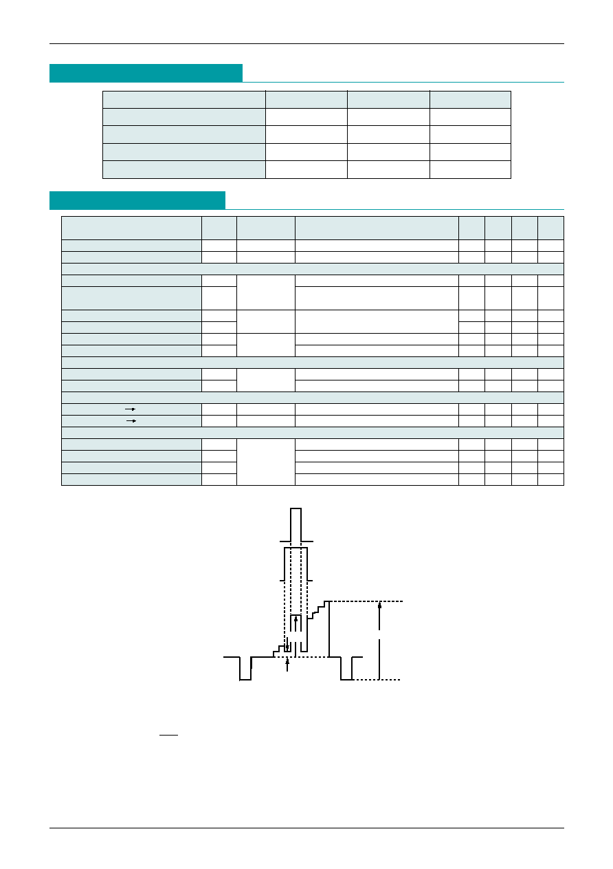
*
1 Input a 1V
P-P
staircase wave to SG1, and pulses as shown in Figure 1 to TP1 and TP3, and measure TP5A.
0V
5V
5V
0V
V
ED
1V
P-P
TP1 waveform
TP3 waveform
TP5A
waveform
V
CH
Figure 1 TP1, TP3, TP5A waveforms
*
2 Given input signal as V1 and output signal as V2, C
T
is obtained as follows.
V2
C
T
=20log dB
V1
*
3 Character switching pin (Pin 1) high level voltage
*
4 Character switching pin (Pin 1) low level voltage
*
5 Border switching pin (Pin 3) high level voltage
*
6 Border switching pin (Pin 3) low level voltage