 | ÐлекÑÑоннÑй компоненÑ: MM1291AF | СкаÑаÑÑ:  PDF PDF  ZIP ZIP |
Äîêóìåíòàöèÿ è îïèñàíèÿ www.docs.chipfind.ru
MITSUMI
Protection of Lithium Ion Batteries (one cell) MM1291
Protection of Lithium Ion Batteries (one cell)
Monolithic IC MM1291
Outline
1-Cell Protection ICs
This is a protection IC for one-cell series that protects lithium ion batteries during excess charging,
discharging, or overcurrent. If abnormalities occur during charging and excess voltage is applied, it has a
function that turns off the external FET switch when voltage is applied to each battery beyond a specified time
(overcharging detection). It also has a function that turns off the external FET switch when the voltage for
each battery falls below a set voltage, to prevent excess discharge when discharging the battery (discharging
detection). At that time, the IC is switched to low current consumption mode. Also, when there is a large
current flow due to shorting or other reasons, there is a functions for turning off the external FET switch
(overcurrent detection). These function comprise a protection circuit, with few external parts, for lithium ion
batteries.
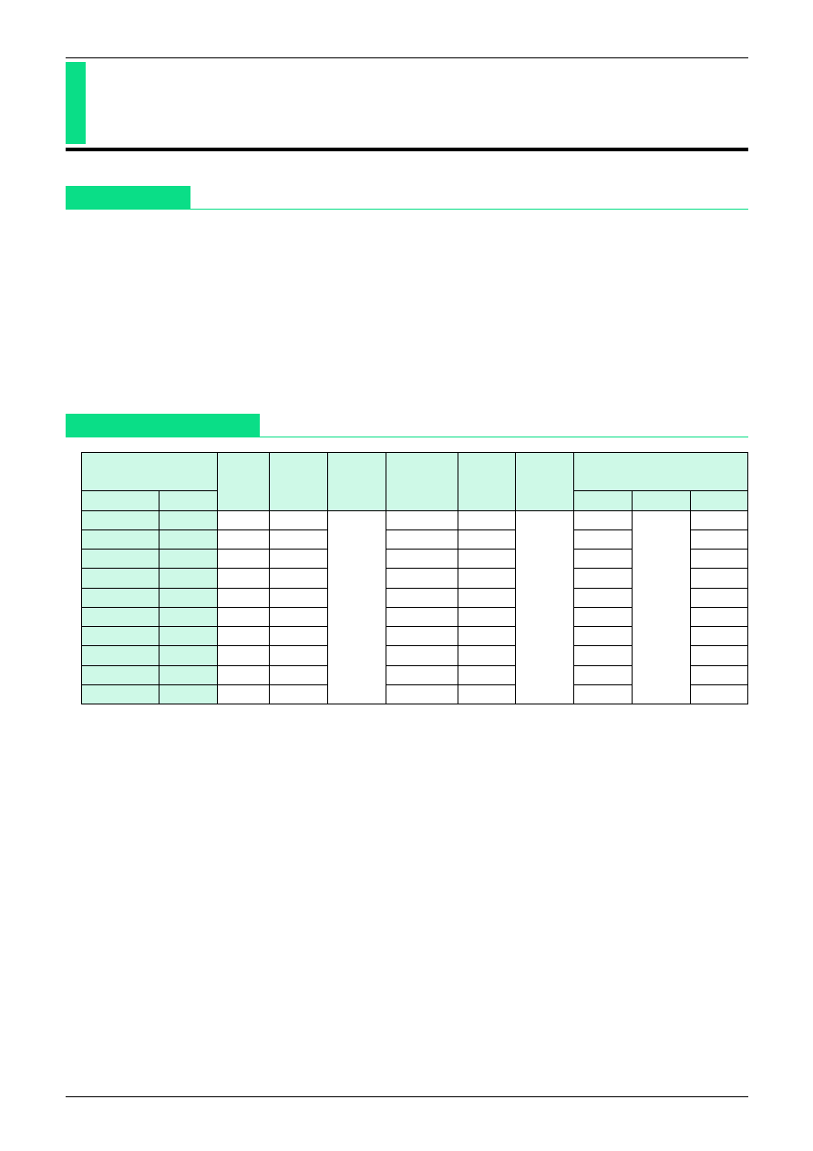
Package
Overcharge
Overdischarge Release
Overcurrent detection
detection Hysteresis Dead time
detection
voltage
Delay
SOP-8
VSOP-8 voltage
Overcurrent Detec time shot-mode
MM1291AF
AW
4.35V
200mV
*
2.6V 2.4V
2.9V
100mV
No
BF
BW
4.25V
200mV
*
2.6V 2.4V
2.9V
100mV
No
CF
4.10V
25mV
*
2.6V 2.4V
2.9V
150mV
No
DF
4.35V
25mV
*
2.6V 2.4V
2.9V
100mV
No
EF
4.35V
27mV
*
2.6V 2.4V
2.9V
100mV
No
GF
4.225V
27mV
*
2.6V 2.4V
2.9V
100mV
No
HF
HW
4.35V
200mV
*
2.6V 2.4V
2.9V
50mV
0.45V
JW
4.25V
270mV
2.3V
2.9V
125mV
0.45V
KF
4.25V
200mV
2.3V
2.9V
50mV
0.9V
MW
4.30V
270mV
2.3V
2.9V
125mV
0.45V
at
Ctd=
0.082µF
min. 0.5S
typ. 1S
max. 1.5S
min. 5mS
typ. 10mS
max. 15mS
min. 5mS
typ. 10mS
max. 15mS
Note : Under open-load conditions, returns to normal mode from overcurrent mode.
(For MM1291A to G, J, M, 5M
or higher; for MM1291H, K, 50M
or higher)

MITSUMI
Protection of Lithium Ion Batteries (one cell) MM1291
Features
1. Current consumption (during overcharging)
V
CC
=4.5V
V
CC
pin 40µA typ.
V
IN
pin 3µA typ.
2. Current consumption (normal)
V
CC
=3.5V
V
CC
pin 7µA typ.
V
IN
pin 2µA typ.
3. Current consumption (during excess discharge)
V
CC
=1.9V
0.7µA typ.
4. Consumption current (during excess discharge)
V
CC
=1.0V
0.17µA max.
5. Overcharge detection voltage (Ta=-20°C~+70°C)
A 4.35V±50mV
B 4.25V±50mV
C 4.10V±50mV
6. Overcharge detection hysteresis
A 200mV typ.
B 200mV typ.
C 27mV typ.
7. Overcharge non-induction time
C
TD
=0.082µF
1S typ.
8. Excess discharge voltage 1
V
CS
=0V
2.6V±0.1V
9. Excess discharge voltage 2
V
CS
=0.05V
2.4V±0.1V
10.Excess discharge reset voltage
2.9V±0.12V
11.Excess discharge during non-induction
10mS typ.
12.Overcurrent detection voltage
A 100mV±10mV
B 100mV±10mV
C 150mV±15mV
13.Reset after overcurrent detection
load release
14.Overcurrent detection non-induction time
10mS typ.
Package
SOP-8C, SOP-8D (MM1291 F)
VSOP-8A (MM1291 W)
*
The box represents the rank resulting from the combination of protection functions.
Applications
1. Cellular phones
2. PHS
3. MD
4. others

MITSUMI
Protection of Lithium Ion Batteries (one cell) MM1291
Pin Assignment
1
4
3
2
8
5
6
7
SOP-8C/SOP-8D
1
GND
2
GD
3
CS
4
OC
5
CE
6
TD
7
V
CC
8
V
IN
Pin Description
Pin N
O
.
N
AME
I/O
Description
1
GND
Input
Negative power supply for this IC. Also acts as detection pin for the battery
connected between V
IN
-GND.
2
GD
Output
Nch-FET gate connection pin for discharge control. Switches gate OFF when
excess discharge is detected, and for current protection. Switches gate ON when
excess discharge is detected in normal state.
3
CS
Input
Detection pin for voltage between CS-GND. Detects excess discharge using Nch-
FET (discharge control) ON resistor and discharge current.
4
OC
Output
Control pin for Nch-FET for charge control. Switches FET off by activating an
external transistor when excess charging is detected.
5
N.C
6
TD
Input
This pin sets non-induction time for overcharge detection. It charges the capacitor
connected between TD-GND with a fixed current during overcharging.
7
V
CC
Input
Positive power supply pin for the IC.
8
V
IN
Input
Detection pin for the battery connected between V
IN
-GND.
MITSUMI
Protection of Lithium Ion Batteries (one cell) MM1291
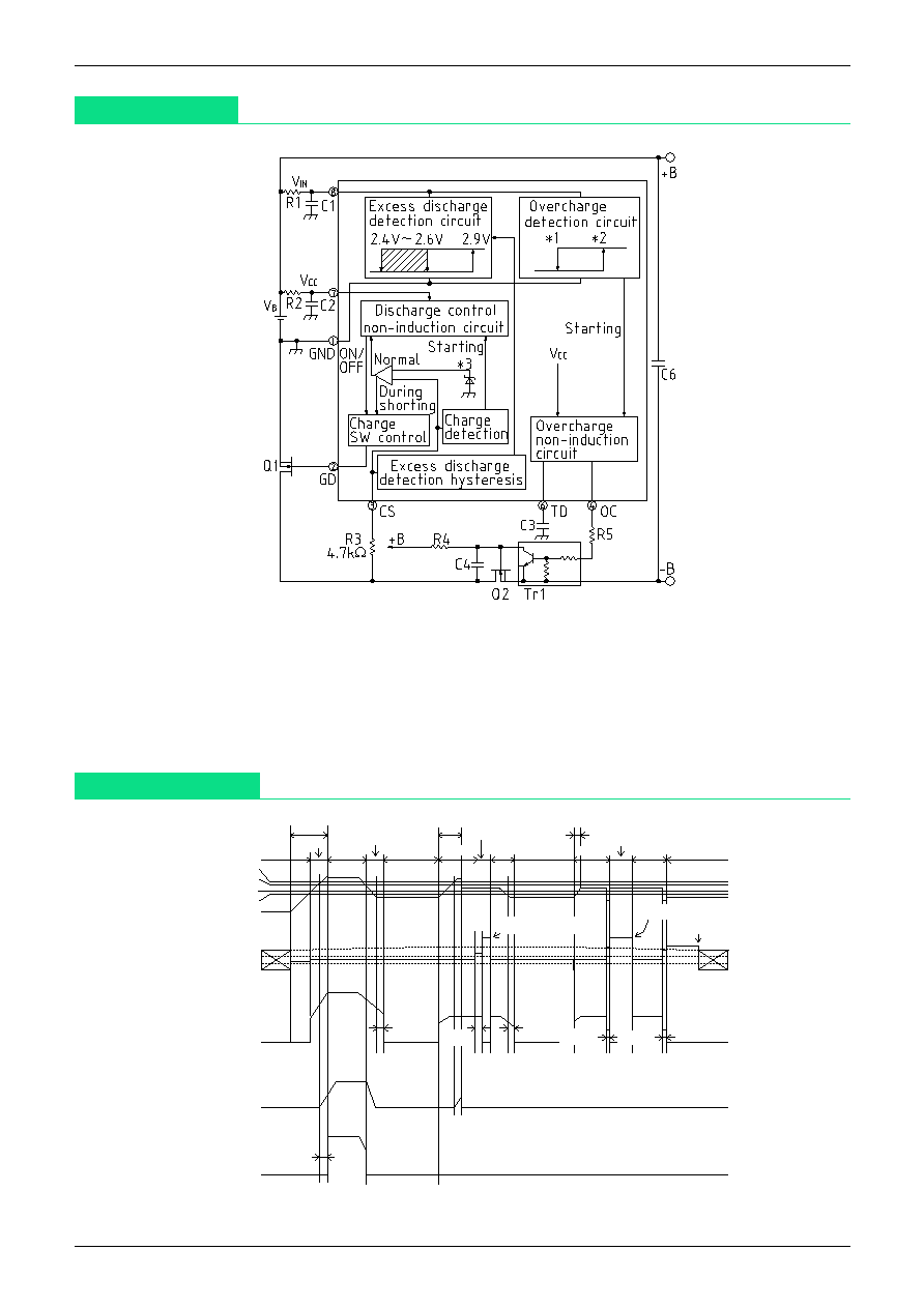
Block Diagram
Timing Chart
V
S
indicates average values.
V
ALML
is low due to the effect of R1 linked to the V
IN
pin.
*
1
A : 4.150V
*
2
A : 4.350V
*
3
A : 0.10V
B : 4.050V
B : 4.250V
B : 0.10V
C : 4.073V
C : 4.100V
C : 0.15V
*
1
unsettled
unsettled
Excess
discharge
Excess
Charge
Excess
discharge
Normal
Normal
Normal
Normal
Charge
Charge
Charge
Normal
Overcurrent protection
Overcurrent protection
Normal
Excess
discharge
Excess discharge
Load release
Load release
Load release
TOD
TOC1
TOC2
TOC2
TOO
T
ALM
0V
V
ALM
V
ALML
V
DF
V
S1
0V
1.0V
V
CS
V
ST
0V
0V
0V
V
IN
(V
CC
)
CS
GD
TD
OC
*
1 C only
MITSUMI
Protection of Lithium Ion Batteries (one cell) MM1291
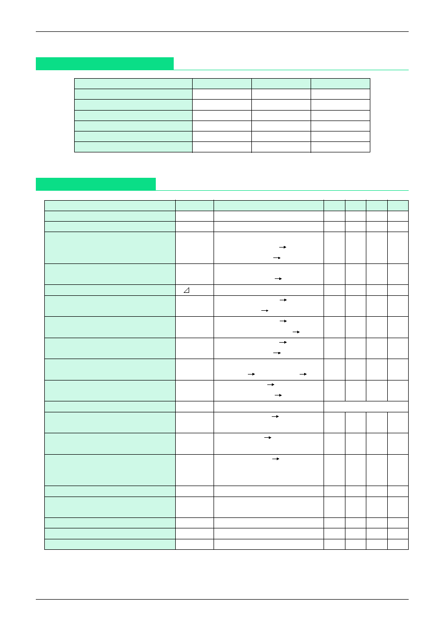
Absolute Maximum Ratings
(Ta=25°C)
Item
Symbol
Rating
Units
Storage temperature
T
STG
-40~+125
°C
Operating temperature
T
OPR
-20~+70
°C
Power supply voltage
V
CC
-0.3~+18
V
V
CC
-OC pin voltage
V
OC
-18~0
V
CS pin voltage
V
CS
-0.6~V
CC
V
Allowable loss
P
D
300
mV
Electrical Characteristics
(Unless otherwise specified Ta=25°C, V
CC
=V
IN
=3.5V, V
CS
=0V, Measurement circuit 1, SW1 : a)
Item
Symbol
Measurement Conditions
Min. Typ. Max. Units
1 (Normal mode) (I
S
1=I
CC
+I
IN
)
I
CC
1
V
CC
=V
IN
=3.5V
8.0
11.0
µA
Consumption current 2 (Overdischarge mode)
I
OP
2
V
CC
=V
IN
=1.9V
0.7
1.0
µA
Ta=-20°C~70°C
Overcharge detection voltage
V
ALM
V
CC
=V
IN
=4.0V 4.5V
4.300 4.350 4.400
V
V
OC
: L H
Overcharge reset voltage
V
ALML
V
CC
=V
IN
=4.5V 4.0V
4.050 4.150 4.240
V
V
OC
: H L
Overcharge hysteresis voltage
V
ALM
V
OC
-V
OCR
150
200
250
mV
Excess discharge detection voltage 1
V
S
1
V
CC
=V
IN
=3.1V 2.0V
2.50
2.60
2.70
V
V
GD
: H L, V
CS
=0V
Excess discharge detection voltage 2
V
S
2
V
CC
=V
IN
=3.1V 2.0V
2.30
2.40
2.50
V
V
CS
=0.05V, V
GD
: H L
Excess discharge reset voltage
V
ODR
V
CC
=V
IN
=2.0V 3.1V
2.78
2.90
3.02
V
V
GD
: L H
Starting voltage
V
ST
V
CC
=V
IN
=2.75V
V
CS
=0V -0.5V, V
GD
: L H
-0.3
-0.1
V
Overcurrent detection voltage
V
CS
V
CS
=0V 0.12V
90
100
110
mV
V
GD
: H L
Overcurrent protection release
load release (more than 5 MEG)
Excess discharge detection
t
OD
V
CC
=V
IN
=3.0V 2.4V,
*
1
5.0
10.0
15.0
mS
non-induction time
measurement circuit 2, SW1 : b, SW2 : a
Excessive current detection during
V
CS
=0V V
CS
,
*
1
5.0
10.0
15.0
mS
non-induction time
t
OC
1
measurement circuit 2, SW1 : a, SW2 : b
V
CC
=V
IN
=4.0V 4.5V,
*
1
Overcurrent non-induction time
t
ALM
measurement circuit 2, SW1 : b, SW2 : a
0.5
1.0
1.5
S
C
TD
=0.082µF
Operating limit voltage
*
2
V
OP
V
CC
When V
GDL
2 > 0.4V
1.2
V
GD pin output voltage H
V
GDH
V
CC
=V
IN
=3.5V
V
GD pin output voltage L1
V
GDL
1
V
CC
=V
IN
=3.5V, V
CS
=0.5V
0.1
0.3
V
GD pin output voltage L2
V
GDL
2
V
CC
=V
IN
=1.5V
0.2
0.4
V
OC pin output current
I
OC
V
CC
=V
IN
=4.5V, SW1 : b
-30
uA
V
CC
-0.3
V
CC
-0.1
MM1291AFBE
*
The CS pin will not cause abnormal operation when connected to protection resistor R
CS
(=4.7k
)
*
1 Refer to input waveforms.
*
2 Operation is unstable below the operating limit voltage.