 | –≠–ª–µ–∫—Ç—Ä–æ–Ω–Ω—ã–π –∫–æ–º–ø–æ–Ω–µ–Ω—Ç: MM1332G | –°–∫–∞—á–∞—Ç—å:  PDF PDF  ZIP ZIP |

MITSUMI
Control of Lithium Ion Batteries Charging (one cell ~ three cells) MM1332
Control of Lithium Ion Batteries Charging (one cell ~ three cells)
Monolithic IC MM1332
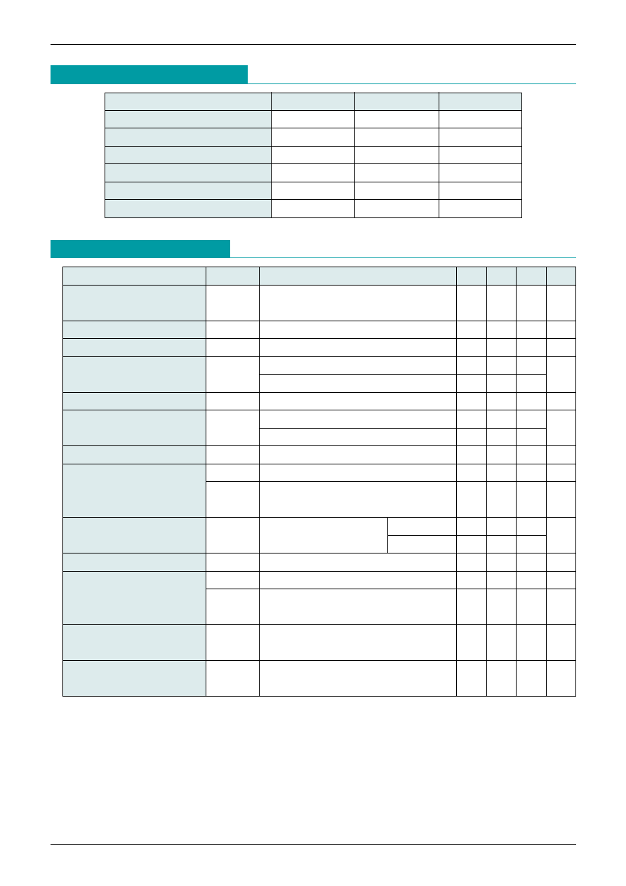
Outline
Series Table
Temperature conditions A: Ta=-25~75∞C, B: Ta=-20~70∞C, C: Ta=0~50∞C,
D: Ta=0~40∞C
This IC is a high precision constant voltage constant current power source controller for lithium ion batteries
serving as power drivers for P-MOS FET. It was developed for use with one to three cell chargers, and the
constant current value can be set freely with external resistance. It has a built-in amplifier for detecting low
battery voltage. Using this IC enables the easy addition of a lithium ion battery charging function to
conventional battery-charging devices.
Features
1. Output voltage (Ta=-20∞C+~70∞C)
3Cell : 12.3V/12.6V±150mV
2Cell : 8.2V/8.4V±100mV
1Cell : 4.1V/4.2V±50mV
2. Current consumption
250µA typ.
3. Constant current output
set by external resistance
Current limit (reference voltage)
0.1V=external resistance current value
4. Low voltage detection function (LV)
2.0V/cell
Package
SOP-8C, SOP-8E (MM1332 F)
*
The box represents the output (charging) voltage rank.
Applications
1. For charging lithium ion batteries
2. High-precision
Stable power sources for all types of equipment
Package
SOP-8C, 8E VSOP-8A, 8B TSOP-16A TSOP-24A
AF
4.100±0.050
B
1cell
BF
8.200±0.100
B
2cell
CF
12.300±0.150
B
3cell
MM1332
DF
4.200±0.050
B
1cell
EF
8.400±0.100
B
2cell
FF
12.600±0.150
B
3cell
GF
Variable
Output
voltage (V)
Output
voltage
temperature
conditions
Full charge
detection
voltage (mV)
Over voltage
detection
voltage (v)
Remarks
*
MITSUMI
Control of Lithium Ion Batteries Charging (one cell ~ three cells) MM1332
Electrical Characteristics
(Unless otherwise specified Ta=25∞C, V
CC
=5V/CEL)
Item
Symbol
Measurement Conditions
Min Typ. Max. Units
Operating power supply
V
CC
Minimum value is during
2.5
5
17.0
V
voltage range
constant-current control
Current consumption 1
I
CC
1
VSW1=VSW2=OV (Charge : ON)
250
µA
Current consumption 2
I
CC
2
VSW1=VSW2=V
CC
(Charge : OFF)
2
µA
Output voltage
V
O
Ta=-20~+70∞C, MM1332A, B, C
4.05
4.10
4.15
V/sell
Ta=-20~+70∞C, MM1332D, E, F
4.15
4.20
4.25
Current limits
V
CL
90
100
110
mV
CEL-CS resistance
R
CEL
MM1332A, B, C
820
k
/sell
MM1332D, E, F
840
SW1 input current
I
SW
1
20
µA
V
L
1
Charge : ON
-0.3
2.0
V
SW1 input voltage
V
H
1
Charge : OFF
VCC
VCC
V
-1.0
+0.3
Low-voltage detection voltage
L
V
A~F Rank
1.90
2.00
2.10
G Rank
2.00
2.15
2.30
V/sell
SW2 input current
I
SW
2
20
µA
V
L
2
Low-voltage detection circuit : ON
-0.3
2.0
V
SW2 input voltage
V
H
2
Low-voltage detection circuit : OFF
VCC
VCC
V
-1.0
+0.3
Low voltage detection
I
LV
0.2
µA
output leak current
Low voltage detection
V
LV
I
SINK
=1mA
0.2
0.4
V
output saturation voltage
*
: MM1332
A : Output voltage 4.1V -for 1cell
B : Output voltage 8.2V -for 2cell
C : Output voltage 12.3V -for 3cell
D : Output voltage 4.2V -for 1cell
E : Output voltage 4.4V -for 2cell
F : Output voltage 12.6V-for 3cell
G : Output voltage available
Absolute Maximum Ratings
(Ta=25∞C)
Item
Symbol
Rating
Units
Storage temperature
T
STG
-40~+125
∞C
Operating temperature
T
OPR
-20~+70
∞C
Power supply voltage
V
CC
max.
-0.3~+18
V
Output voltage
V
O
max.
-0.3~V
CC
V
SW input voltage
V
SW
-0.3~V
CC
+0.3
V
Allowable power dissipation
Pd
300
mW

MITSUMI
Control of Lithium Ion Batteries Charging (one cell ~ three cells) MM1332
Pin Assignment Description
1
4
3
2
8
5
6
7
SOP-8C/SOP-8E
Pin No. Name
I/O
Description
1
SW1
Input
2
SW2
Input
3
LV
Output
4
GND
5
CS
Input
6
CEL
Input
7
EXT
Output
8
V
CC
Charging ON/OFF control input pin.
SW1=V
CC
: OFF, SW1=GND : ON
Goes OFF when open as it is pulled up to V
CC
.
Low voltage detection circuit ON/OFF control input pin.
SW2=V
CC
: OFF, SW2=GND : ON
Goes OFF when open as it is pulled up to V
CC
.
Low voltage detection circuit output pin.
NPN-Tr open collector output; goes ON (low level) for low voltage.
Ground pin.
Current detection pin. Detects current when external resistor voltage drops and
controls current. Reference voltage 0.1V=external resistance current value
Battery voltage input pin
*
Six types depending on rank : 4.1V, 8.2V, 12.3V, 4.2V, 8.4V, 12.6V, (TYP.)
Constant voltage circuit output pin. Controls external P-MOS FET gate and
charges constant voltage.
Power supply input pin.
*
G : Constant voltage circuit input pin
External resistance ratio (R1 : R2) enables setting constant voltage circuit output voltage.
Low voltage detection voltage is set for one cell (4.1V or 4.2V).
Pin Description

MITSUMI
Control of Lithium Ion Batteries Charging (one cell ~ three cells) MM1332
Block Diagram
MM1332A, B, C, D, E, F,
MM1332G

MITSUMI
Control of Lithium Ion Batteries Charging (one cell ~ three cells) MM1332
Timing Chart
CEL<Lv (When Low Voltage Detection Voltage)
V
CC
SW1
SW2
CEL
CS
LV
Charge ON
VH1 (V
CC
-1.0~V
CC
+0.3)
VL1 (-0.3~2.0V)
VH2 (V
CC
-1.0~V
CC
+0.3)
VL2 (-0.3~2.0V)
VCL (100mV typ.)
With LV pulled up to V
CC
by a resistance
Charge OFF
Low Voltage
Detection Circuit ON
CEL<Lv (Low Voltage Detection Voltage)