 | –≠–ª–µ–∫—Ç—Ä–æ–Ω–Ω—ã–π –∫–æ–º–ø–æ–Ω–µ–Ω—Ç: MM1357 | –°–∫–∞—á–∞—Ç—å:  PDF PDF  ZIP ZIP |

MITSUMI
Control of Lithium Ion Batteries (switching regulator secondary) (two cells) MM1357
Control of Lithium Ion Batteries (switching regulator secondary) (two cells)
Monolithic IC MM1357
Outline
This IC is used to control two-cell chargers and the secondary side of switching regulators; it features
enhanced functions for current switching and for overcharge detection and other kinds of protection. The
control output is capable of driving a photocoupler LED. The charging current can be switched between high
and low currents, and each can also be varied externally.
Features
1. Charging voltage
: Can be set externally
2. Charging current (switchable between high and low levels, variable)
High : 320mV typ.
Low : 145mV typ.
3. Reference voltage
: 1.207V typ.
Package
SOP-14B
Applications
1. Switching regulator
2. AC adapter
3. Lithium ion battery charger
MITSUMI
Control of Lithium Ion Batteries (switching regulator secondary) (two cells) MM1357
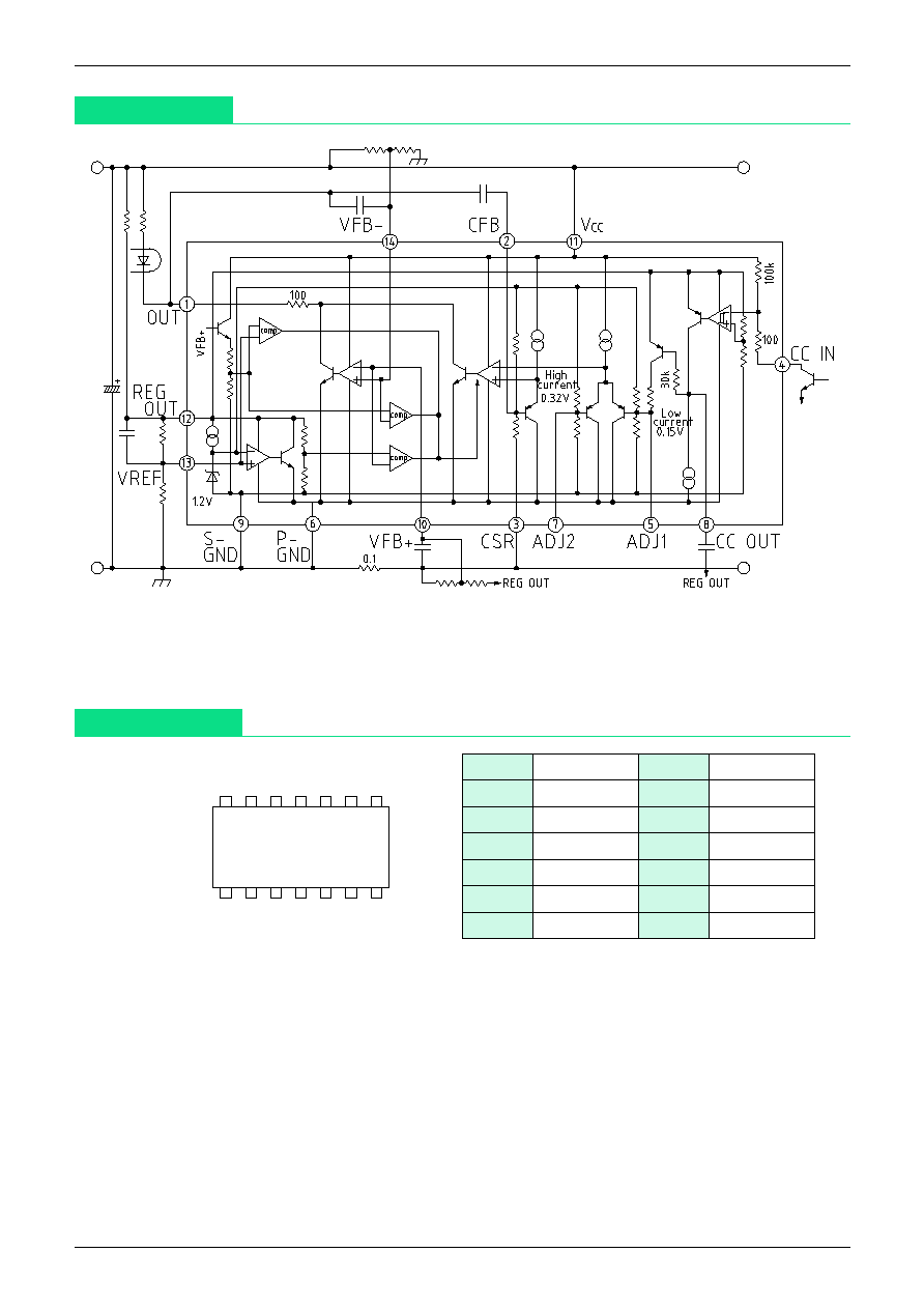
Pin Assignment
SIP-14B
1
3
6
2
4
5
7
14
11
9
13 12
10
8
1
OUT
8
CC OUT
2
CFB
9
S-GND
3
CSR
10
VFB+
4
CC IN
11
V
CC
5
ADJ1
12
REG OUT
6
P-GND
13
VREF
7
ADJ2
14
VFB-
Block Diagram

MITSUMI
Control of Lithium Ion Batteries (switching regulator secondary) (two cells) MM1357
Item
Symbol
Ratings
Units
Storage temperature
T
STG
-40~+125
∞C
Operating temperature
T
OPR
-20~+85
∞C
Power supply voltage
V
CC
max.
-0.3~+24
V
Allowable loss
P
D
350
mW
Absolute Maximun Ratings
Pin Description
Pin no. Pin name Input/output
Function
1
OUT
Output
Output pin for charging control
An external photocoupler is controlled for constant-current, constant-voltage charging control.
Amp inverting input pin for current control
An external capacitor (approx. 0.1 µF) is connected between CFB and OUT, and
phase compensation used to improve oscillation.
2
CFB
Input
Current detection pin
Current is detected via the voltage drop across an external resistance between
CSR and GND (R1), to control the charging current.
3
CSR
Input
Charging current switching signal input pin
H (V
CC
) is the charging current 0.15V/R1, and L (GND) is the charging current
0.32V/R1. If for instance R1 is 0.1
, then switching is between 1.5A and 3.2A (typ.).
The switching voltage VTH is as follows.
When REG OUT is 2.5V, V
TH
is 2.05V typ.
When REG OUT is 4V, V
TH
is 3.0V typ.
When REG OUT is 5V, V
TH
is 3.7V typ.
4
CC IN
Input
Amp non-inverting input pin 1 for current control
The pin voltage is set at 0.15V typ. With CC-IN at H or open, the non-inverting input
pin of the current control amp is at 0.15 V.
By adjusting the pin voltage using an external resistance or by other means, the
charging current can be varied.
5
ADJ1
Input
6
P-GND
Input
Power ground pin
Amp non-inverting input pin 2 for current control
The pin voltage is set at 0.32V typ. With CC-IN at L, the non-inverting input pin of the
current control amp is at 0.32V.
By adjusting the pin voltage using an external resistance or by other means, the
charging current can be varied.
7
ADJ2
Input
8
CC OUT
Output
Charging current switching signal output pin
Output is in phase with CC IN. By connecting an external capacitor between CC OUT
and REG OUT, a delay can be added only when the current switching CC IN goes
from H to L. For instance, when REG OUT is 4V, on connecting an 0.1µF capacitor
CC OUT becomes about 50mS (an example is shown in the Timing Chart section).
9
S-GND
Input
Signal ground pin
10
VFB+
Input
Amp non-inverting input pin for voltage control
The charging voltage is set through the resistances at the VFB + pin and the VFB - pin.
11
V
CC
Input
Power supply input pin
12
REG OUT
Output
Reference voltage circuit output pin
The reference voltage can be set between 2 and 6V. The input current to start the
reference voltage should be set to 1mA or greater.
13
VREF
Input
Reference voltage circuit input pin
The VREF pin voltage is set at 1.2V typ. The REG OUT voltage can be set through the
resistances between REG OUT and VREF, and between VREF and GND.
Amp inverter input pin for voltage control
14
VFB-
Input
Amp inverting input pin for voltage control
The charging voltage can be set through the resistances at the VFB + pin and VFB - pin.
By connecting an external capacitor (approx. 0.1µF) between VFB and OUT for phase
compensation, oscillation can be improved.
MITSUMI
Control of Lithium Ion Batteries (switching regulator secondary) (two cells) MM1357
Timing Chart
Timing chart for connection of a timing capacitor C
T
to CC OUT
With REG OUT at 4V and C
T
=0.1µF, TD is approx. 50mS.
8.4V
4V
0.15V
CC IN
Low-current
mode
High-current
mode
CC OUT
V
TH
V
TH
0.32V
0
V
TH
level
0
CC-IN
CC-OUT
CSR
V
TH
level
TD
Electrical Characteristics
(Except where noted otherwise, Ta=25∞C, REG OUT=4V, V
CC
=8.4V)
Item
Symbol
Measurement conditions
Min. Typ. Max. Units
V
CC
minimum input current
I
CC
Excluding REG OUT input current
0.25
0.40
mA
Amp input for voltage control
Input offset voltage
V
IO
1
5
mV
Input bias current VFB+
I
B+
20
250
nA
Input bias current VFB-
I
B-
20
250
nA
Common-mode input voltage range
V
I
*
0.7
REG OUT
-0.7
V
Amp input for current control
ADJ1 pin input impedance
R
ADJ
1
13
k
ADJ2 pin input impedance
R
ADJ
2
13
k
CFB pin input impedance
R
CFB
2
k
Current limit 1
V
CL
1
High-current mode
310
320
330
mV
Current limit 2
V
CL
2
Low-current mode
137
145
153
mV
OUT pin input current 1
I
S
1
OUT=8.4V (voltage-control amp)
20
mA
OUT pin input current 2
I
S
2
OUT=4 V (voltage-control amp)
20
mA
OUT pin leakage current
I
L
OUT=24V
2
µA
CC IN input impedance
R
CI
100
k
CC switching voltage L (VTR mode)
V
CL
2.6
V
CC switching voltage H (CHG mode)
V
CH
3.4
V
CC OUT output intake current
I
CO
1
On switching from low to high current mode
6
µA
CC OUT output current
I
CO
2
On switching from high to low current mode
0.5
mA
CC OUT output voltage range
V
CO
0.4
3.6
V
Reference voltage
V
REF
1.195 1.207 1.219
V
REG OUT output voltage variable range
V
REG
2.0
6.0
V
REG OUT maximum input current
I
max.
20
mA
REG OUT minimum input current
I
min.
1.0
mA
*
Because there is an internal circuit for protection against shorts of external components, the common-mode
input voltage range is 0.7V to REG OUT-0.7V. Values are set such that overvoltages do not occur when
there is a short between VBF+ and REG OUT or between VFB- and GND.
Recommended Operating Conditions
Item
Symbol
Ratings
Units
Operating temperature
T
OPR
-15~+80
∞C
Operating voltage
V
OPR
+2~+20
*
V
*
The minimum operating voltage is under constant-current control

MITSUMI
Control of Lithium Ion Batteries (switching regulator secondary) (two cells) MM1357
Note 1 : 1. The REG OUT voltage can be set to 1.2V typ. (R5+R6)/R6. (REG OUT = 2 to 6V)
2. The value of R4 should be set according to the load. (Consider it to be a shunt regulator.)
3. The voltage under constant-voltage charging is equal to (R3/R2) REG OUT. When a high-
precision voltage is required, use the knob for adjustment.
4. The current in constant-current charging can be set to either of two values, 0.15V/R1 (when CC-IN
is H), and 0.32V/R1 (when CC-IN is L).
5. R7 is a resistance for current limiting.
6. The capacitors C1 and C5 are to prevent oscillation; C4 is for soft starting of the REG OUT
voltage; and C2 is used to delay current switching (CC-OUT switched from H to L).
Note 2 : This IC incorporates a voltage-controlling amp and protection against shorting to VREF ; when R2,
R3, R5 and R6 are shorted, the voltage is limited to its minimum value. By means of a comparator
within the VFB+, VFB- and VREF pin area, upon resistance shorting the OUT pin is forced to L.
Note 3 : The above diagram is an example for reference purposes; in actual use the circuit should be studied
thoroughly prior to use.
Application Circuits
Characteristics
Current limit 1 vs temperature
0.35
0.3
0.25
-25
0
25
50
75 85
Ambient temperature (
∞
C)
Current limit 1 (V)
Current limit 2 vs temperature
0.2
0.15
0.1
-25
0
25
50
75 85
Ambient temperature (
∞
C)
Current limit 2 (V)

MITSUMI
Control of Lithium Ion Batteries (switching regulator secondary) (two cells) MM1357
CC switching voltage vs temperature
REG OUT=4V
3.5
3
2.5
-25
0
25
50
75 85
Ambient temperature (
∞
C)
CC IN, L H
CC IN, H L
CC switching voltage (V)
CC switching voltage vs REG OUT voltage
5
4
3
2
1
0
2
3
4
5
6
REG OUT voltage (V)
CC IN, L H
CC IN, H L
CC switching voltage (V)
CC OUT-DELAY TIME Ta=25∞C REG OUT=4V
(C
T
is the capacitance between CC OUT and REG OUT)
5
4
3
2
1
0
-1
0
20
40
60
100
80
120
TIME (mS)
CT=0.1
µ
F
CT=0.047
µ
F
CT=0
µ
F
CC OUT (V)
CC OUT intake current vs temperature
8
6
10
4
0
2
-25
0
25
50
75 85
Ambient temperature (
∞
C)
CC OUT intake current (
µ
A)
REG OUT voltage vs REG OUT input current Ta=25∞C
5
4
3
2
1
0
0.1
1
10
100
REG OUT input current (mA)
REG OUT voltage (V)
Reference voltage vs temperature
1.22
1.21
1.2
-25
0
25
50
75 85
Ambient temperature (
∞
C)
Reference voltage (V)
REG OUT voltage (4V)- temperature
4.05
4
3.95
-25
0
25
50
75 85
Ambient temperature (
∞
C)
REG OUT input current10mA
REG OUT voltage (4V) (V)