 | –≠–ª–µ–∫—Ç—Ä–æ–Ω–Ω—ã–π –∫–æ–º–ø–æ–Ω–µ–Ω—Ç: MS6260MU | –°–∫–∞—á–∞—Ç—å:  PDF PDF  ZIP ZIP |

MO
SA
MS6260
Gain And Attenuation Volume Controller IC
REV 1 1 www.mosanalog.com.tw
Gain and Attenuation Volume Controller IC
One Set of Stereo Input, Low voltage
Gain and Attenuation 15~-79dB, Good PSRR
FEATURES
Operation range: 2.7V~5.5V
Low power consumption
Gain/Attenuation: 15dB to ≠79dB at 1dB/step
Good PSRR and low pop noise
Housed in 10 pin MSOP package
I
2
C interface
APPLICATIONS
Multimedia system
Hi-Fi audio system
MP3, PDA
DESCRIPTION
The MS6260 is the stereo audio volume controller IC. It uses CMOS technology specially for the low voltage
application with low noise, rail-to-rail output. The MS6260 provide an I
2
C control interface with gain / attenuation
range of 15dB to ≠79dB, 1dB/step. The excellent power supply ripple reject is a good for audio system. The initial
condition is set to be maximum attenuation ≠79dB and mute on mode when power on.
PIN CONFIGURATION
Symbol Pin
Description
A.O.
1
Address option *
L-IN
2
Left channel input
L-OUT
3
Left channel output
V
SS
4 Ground
SDA 5
I
2
C data input
SCL 6
I
2
C clock input
V
DD
7
Positive supply voltage
R-OUT
8
Right channel output
R-IN
9
Right channel input
V
REF
10
Reference voltage = 1/2V
DD
9
8
7
10
2
3
4
1
R-IN
R-OUT
V
DD
SCL
L-IN
L-OUT
V
SS
SDA
5
6
MS6260
A.O.
V
REF
Note: 1. Pin 1 is set to Lo or open , the address code is 88H (10001000B).
2. Pin 1 is set to Hi , the address code is 8CH (10001100B).
3. The V
REF
connects a capacitor to Vss.

MO
SA
MS6260
Gain And Attenuation Volume Controller IC
REV 1 2 www.mosanalog.com.tw
BLOCK DIAGRAM
I2C Interface
-10dB/STEP
-1dB/STEP
1dB/STEP
Serial Bus Decoder and Latches
Reference
Circuit
1dB/STEP
-1dB/STEP
-10dB/STEP
L-IN
R-IN
REF
SDA
SCL
V
REF
R-OUT
L-OUT
ORDERING INFORMATION
Package
Part number
Packaging Marking
Transport Media
10-Pin MSOP
MS6260MTR
6260
3.5k Units Tape and Reel
10-Pin MSOP
MS6260MU
6260
80 Units Tube
10-Pin MSOP (lead free)
MS6260MGTR
6260G
3.5k Units Tape and Reel
10-Pin MSOP (lead free)
MS6260MGU
6260G
80 Units Tube
ABSOLUTE MAXIMUM RATINGS
Symbol
Parameter Rating
Unit
V
DD
Supply
Voltage
6
V
V
ESD
Electrostatic Handling
-4500 to 4500
V
T
STG
Storage Temperature Range
-65 to 150
T
A
Operating Ambient Temperature Range
-40 to 85
T
J
Maximum Junction Temperature
150
T
S
Soldering Temperature, 10 seconds
260
R
THJA
Thermal Resistance from Junction to Ambient in Free Air
MSOP10
194
/W
OPERATING RATINGS
Symbol Parameter Min Typ Max Unit
V
DD
Supply Voltage
2.7
-
5.5
V
MO
SA
MS6260
Gain And Attenuation Volume Controller IC
REV 1 3 www.mosanalog.com.tw
5V ELECTRICAL CHARACTERISTICS
(V
DD
=5.0V, V
SS
=0V, Attenuation=0dB, Gain=0dB, f=1kHz, V
O
=0dBV, V
REF
Cap=10uF; unless otherwise specified)
Symbol Parameter
Conditions Min
Typ
Max
Unit
DC Characteristics
I
Q
Quiescent current
-
3.8
4.2
mA
Max gain
-
15
-
dB
A
GA
Gain/Attenuation
Max attenuation
-
-79
-
dB
A
STEP
Gain/Attenuation step
-
1
-
dB
E
GA
Gain/Attenuation step error
-
0.3
-
dB
E
IGA
Interchannel gin/attenuation error
-
0.3
-
dB
CS Channel
separation
95 105 - dB
PSRR
Power supply rejection ratio
Vripple = -20dBV, 100Hz
-
53
-
dB
MUTE Mute
Attenuation
Vin=0dBV
-
85
-
dB
Rin Input
Impedance
18 20 - k
Rout Output
Impedance
-
50 100
AC Characteristics
Vo
Maximum output voltage swing
(THD+N)/S < 0.1%
-
4.8
-
Vpp
THD+N
Total harmonic distortion plus
noise
-
-69
-64
dB
S/N Signal-to-noise
ratio
V
O
=4.5Vpp 95
100
-
dB
Bus Characteristics
V
IH
Bus high input level
-
-
0.7V
DD
V
V
IL
Bus low input level
0.3V
DD
- - V
3.3V ELECTRICAL CHARACTERISTICS
(V
DD
=3.3V, V
SS
=0V, Attenuation=0dB, Gain=0dB, f=1kHz, V
O
=-3dBV, V
REF
Cap=10uF; unless otherwise specified)
Symbol Parameter
Conditions Min
Typ
Max
Unit
DC Characteristics
I
Q
Quiescent current
-
3.7
4.1
mA
CS Channel
separation
90 100 - dB
PSRR
Power supply rejection ratio
Vripple = -20dBV, 100Hz
-
52
-
dB
MUTE Mute
Attenuation
Vin=-3dBV
-
80
-
dB
AC Characteristics
Vo
Maximum output voltage swing
(THD+N)/S < 0.1%
-
3
-
Vpp
THD+N
Total harmonic distortion plus
noise
-
-69
-64
dB
S/N Signal-to-noise
ratio
85 90 - dB

MO
SA
MS6260
Gain And Attenuation Volume Controller IC
REV 1 4 www.mosanalog.com.tw
2.7V ELECTRICAL CHARACTERISTICS
(V
DD
=2.7V, V
SS
=0V, Attenuation=0dB, Gain=0dB, f=1kHz, V
O
=-3dBV, V
REF
Cap=10uF; unless otherwise specified)
Symbol Parameter
Conditions Min
Typ
Max
Unit
DC Characteristics
I
Q
Quiescent current
-
3.2
3.6
mA
CS Channel
separation
90 100 - dB
PSRR
Power supply rejection ratio
Vripple = -20dBV, 100Hz
-
50
-
dB
MUTE Mute
Attenuation
Vin=-3dBV
-
80
-
dB
AC Characteristics
Vo
Maximum output voltage swing
(THD+N)/S < 0.3%
-
2
-
Vpp
THD+N
Total harmonic distortion plus
noise
-
-69
-64
dB
S/N Signal-to-noise
ratio
85 90 - dB
TYPICAL PERFORMANCE CHARACTERISTICS
(Ta=25, R
L
=10k
, V
REF
Cap=10uF; unless otherwise specified)
THD+N (%)
OUTPUT VOLTAGE (dBV)
THD+N (%)
OUTPUT VOLTAGE (dBV)
THD+N (%)
OUTPUT VOLTAGE (dBV)
THD+N vs. output voltage
THD+N vs. output voltage
THD+N vs. output voltage
f=20Hz
f=20Hz
f=20Hz
f=1kHz
f=20kHz
f=20kHz
f=1kHz
f=1kHz
f=20kHz
V
DD
=5V
V
DD
=2.7V
V
DD
=3.3V
THD+N (%)
FREQUENCY (Hz)
C
H
A
N
N
E
L SEPAR
ATION
(
d
B)
FREQUENCY (Hz)
QUIE
S
C
E
N
T CURRE
NT (mA
)
SUPPLY VOLTAGE (V)
THD+N vs. frequency
Channel separation vs. frequency
Quiescent current vs. supply voltage
V
DD
=5V
V
O
=0dBV
V
DD
=3.3V
V
O
=-3dBV
V
DD
=2.7V
V
O
=-3dBV
V
DD
=5V
V
O
=0dBV
V
DD
=2.7V
V
O
=-3dBV
V
DD
=3.3V
V
O
=-3dBV
MO
SA
MS6260
Gain And Attenuation Volume Controller IC
REV 1 5 www.mosanalog.com.tw
PSR
R
(
d
B)
FREQUENCY (Hz)
PSR
R
(
d
B)
FREQUENCY (Hz)
PSR
R
(
d
B)
FREQUENCY (Hz)
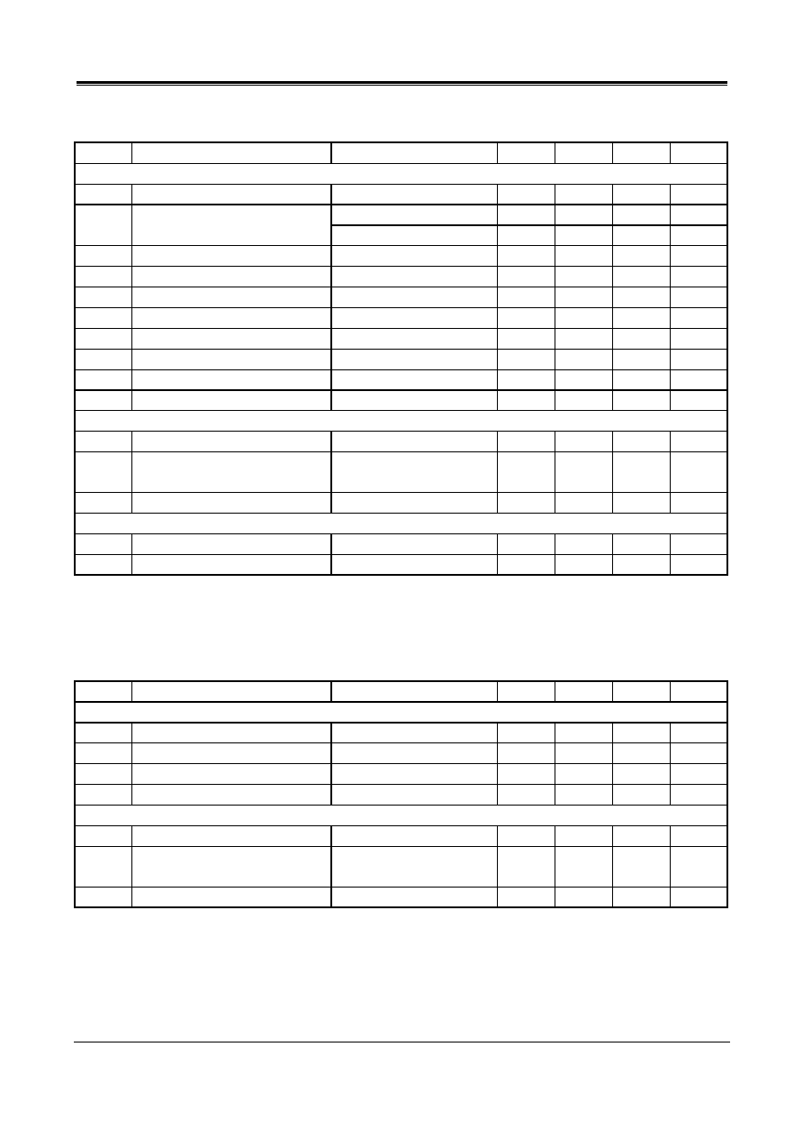
PSRR vs. frequency
PSRR vs. frequency
PSRR vs. frequency
CAP=22uF
CAP=22uF
CAP=22uF
CAP=10uF
CAP=10uF
CAP=10uF
CAP=2.2uF
CAP=2.2uF
CAP=2.2uF
V
DD
=5V
V
RR
=-20dBV
V
DD
=3.3V
V
RR
=-20dBV
V
DD
=2.7V
V
RR
=-20dBV
I
2
C BUS DESCRIPTION
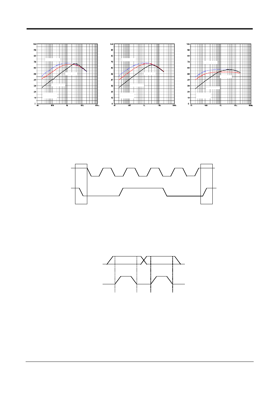
Start and stop conditions
A start condition is activated when the SCL is set to HIGH and SDA shifts from HIGH to LOW state. The stop
condition is activated when SCL is set to HIGH and SDA shifts from LOW to HIGH state. Please refer to the timing
diagram below.
SDA
SCL
Start
Stop
SCL : Serial Clock Line, SDA : Serial Data Line
Data validity
A data on the SDA line is considered valid and stable only when the SCL signal is in HIGH state. The HIGH and
LOW states of the SDA line can only change when the SCL signal is LOW. Please refer to the figure below.
SDA
SCL
Data line
stable,
Data valid
Data
change
allowed
Byte format
Every byte transmitted to the SDA line consists of 8 bits. Each byte must be followed by an acknowledge bit.
The MSB is transmitted first.