
MOSA ELECTRONICS
MS6610
Stereo Audio DAC
- 1 -
www.mosanalog.com.tw
FEATURES
Current output Easy application :
Space saving package(SOP8 ) Operation range: 2.7V~5.5V
Low power consumption Output and bias current are proportional to supply voltage
Low total harmonic distortion
Wide dynamic range(16-bit resolution)
Fast setting time permits 2*, 4*, and 8* oversampling(serial input) or double speed operation at 4* oversampling
Internal bias current ensures maximum dynamic range
Wide operating temperature range of -40 to 85
Internal timing and control circuits
Compatible with most of the Japanese input formats; time multiplexed, two's complement, TTL
No zero crossing distortion
APPLICATIONS
VCD Player, DVD Player.
DESCRIPTION
The MS6610 is a 16-bit current-output Digital-to-Analog Converter(DAC). The MS6610 is fabricated in a 0.8
µ
m
CMOS process and features extremely low power dissipation, small package size and ease of application. The accuracy
of the matched coarse current sources, combined with the unique symmetrical decoding method, preclude zero-crossing
distortion and ensures high quality audio reproduction. These unique features, combined with its exceptional
performance, make the MS6610 ideally suited for use in digital audio equipment. MS6610 is pin and function
compatible with the Philips, TDA1545.
PINNING
Symbol Pin
Description
BCK
1
bit clock input
WS
2
word select input
DATA 3
data
input
GND 4
ground
V
DD
5
positive supply voltage
I
OL
6
left channel output
V
REF
7
reference voltage output
I
OR
8
right channel output
7
6
5
8
2
3
4
1
MS6610
I
OR
V
REF
I
OL
V
DD
BCK
WS
DATA
GND
Pin configuration

MOSA ELECTRONICS
MS6610
Stereo Audio DAC
- 2 -
www.mosanalog.com.tw
BLOCK DIAGRAM
LEFT OUTPUT LATCH
LEFT BIT SWITCHES
11-BIT
PASSIVE
DIVIDER
32 (5-BIT)
MATCHED
CURRENT
SOURCES
Iref
RIGHT OUTPUT LATCH
RIGHT BIT SWITCHES
32 (5-BIT)
MATCHED
CURRENT
SOURCE
11-BIT
PASSIVE
DIVIDER
Iref
LEFT INPUT LATCH
RIGHT INPUT LATCH
CONTROL
&
TIMING
Vref
Vref
REFERENCE
SOURCE
I
BL
Iref I
BR
I
BL
I
BR
-
+
-
+
1
2
3
BCK
WS
DATA
6
8
V
OUT
left
V
OUT
right
5
V
DD
4
OP1
OP2
I
OL
I
OR
1nF C2
3.9K
R2
1nF C1
3.9K
R1
ground
C3
100nF
7
Rref
11K
R4
33K
R3
22K
+
C4
1uF
Vref
Fig.1 Block diagram.
LIMITING VALUES
Symbol
Parameter Min
Max
Unit
V
DD
Positive Supply Voltage
-
6
V
Tsig
Storage Temperature Range
-55
+150
T
XTAL
Maximum Crystal Temperature
-
+150
T
AMB
Operating Ambient Temperature Range
-40
+85
Ves Electrostatic
Handling
-2000
2000 V

MOSA ELECTRONICS
MS6610
Stereo Audio DAC
- 3 -
www.mosanalog.com.tw
ELECTRICAL CHARACTERISTICS
(Ta=25, V
DD
=5V)
SYM PARAMETER CONDITIONS
MIN
TYP
MAX
UNIT
V
DD
Positive Supply Voltage
2.7
5
5.5
V
I
DD
Operating Current
at code 0000H
-
3
5
mA
PSSR
Power Ripple Rejection Ratio
-
30
dB
DIGITAL INPUTS (WS, BCK, DATA)
SYM PARAMETER CONDITIONS
MIN
TYP
MAX
UNIT
f
BCK
Input Clock Frequency
18.4
MHz
BR
Bit Rate Data Input (Pin 3)
18.4
Mbits/s
F
WS
Word Select Input (Pin 2)
384
kHz
t
r
Rise
Time
12
ns
t
f
Fall
Time
12
ns
t
C
r
Bit Clock Cycle Time
54
ns
t
HB
Bit Clock High Time
15
ns
t
LB
Bit Clock Low Time
15
ns
t
SD
Data Set-up Time
12
ns
t
HD
Data Hold Time to Bit Clock
2
ns
t
HW
Word Select Hold Time
2
ns
t
SW
Word Select Set-up Time
12
ns
ANALOG INPUT (Iref)
SYM PARAMETER CONDITIONS
MIN
TYP
MAX
UNIT
Rref
Reference Resistor (Fig.1)
7.4
11.0
14.6
K
ANALOG OUTPUT (I
OL
, I
OR
)
SYM PARAMETER CONDITIONS
MIN
TYP
MAX
UNIT
Res
Resolution
16
bits
V
DCC
DC output Voltage Compliance
2.0
V
DD
-1 V
I
FS
Full Scale Output Current
I
FS = 0.2V
DD
0.9 1.0 1.1 mA
T
CFS
Full Scale Temperature Coefficient at
Analog Outputs ; I
OL
, I
OR
±
400
10-
16
Ptot
Total Power Dissipation
at code 0000H
15
mW
I
bias
Bias Current (adjustable)
643
714
785
µ
A
THD
Total Harmonic Distortion
including noise
-85
-78
dB
at 0 dB
0.005
0.01
THD
Total Harmonic Distortion
including noise
-30
-24
dB
at -60 dB
3
6
S/N
Signal-to-Noise Ratio
a-weighted at code
0000H
92
dB
CS Channel
Separation
95
dB
MOSA ELECTRONICS
MS6610
Stereo Audio DAC
- 4 -
www.mosanalog.com.tw
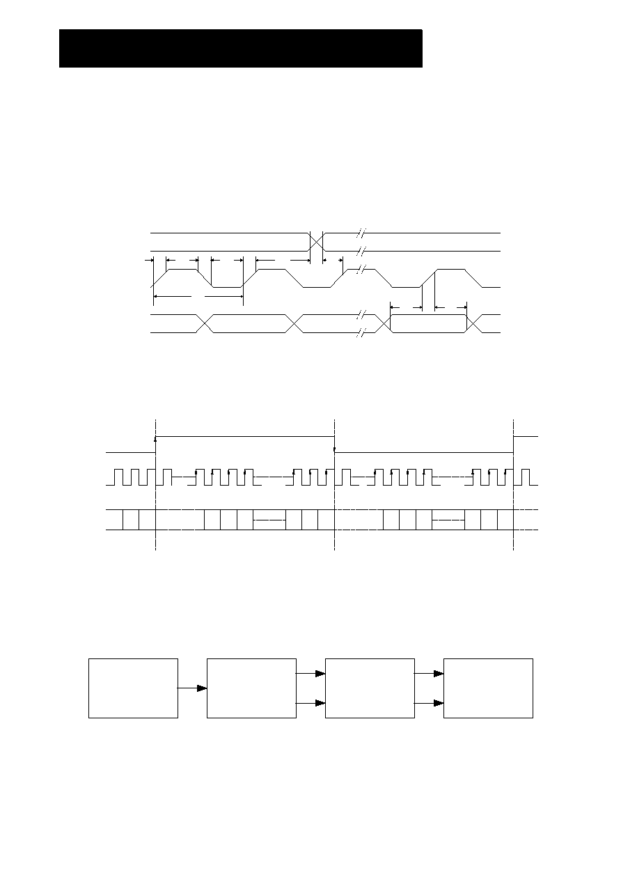
TIMING AND DATA FORMAT
The MS6610 accepts input serial data formats of 16-bit word length. Left and right data words are time
multiplexed. The MSB(bit 1) must always be First. The format of data input is shown in Figs. 2 and 3. With a LOW
level on the word select input(WS) input data is placed in the right input register and with HIGH level on the WS input
data is placed in the left register. The data in the input registers are simultaneously latched in the output registers which
control the bit switches. Internal bias currents IBL and IBR are each added to the full scale output current IFS in order
to achieve the maximum dynamic range at the outputs of OP1 and OP2(Fig. 1). The reference output voltage Vref(Fig.
1) is 2/3 VDD. In this way the maximum dynamic range is achieved over the entire power supply range.
RIGHT
WS
BCK
DATA
LSB
MSB
t
r
t
HB
t
f
t
cr
t
LB
t
HW
t
SW
LEFT
t
SD
t
HD
Fig.2 Timing and input signals.
0
1
2
15
14
13
2
1
0
MSB
LSB
15
14
13
2
1
0
MSB
LSB
RIGHT
LEFT
WS
BCK
DATA
MEASUREMENT BLOCK DIAGRAM
R-ch
L-ch
AC Level (Vrms)
THD
THD+N
Generate
sinewave pattern for
BCK.WS.DATA
MS6610
MS6308
f = 1 kHz , 2Vp-p
sinewave
Pattern
Generator
DAC
OPAmp
Analysis
Equipment
NOTE : THD and THD+N is measured by HP AUDIO ANALYZER and FFT Analysis.

MOSA ELECTRONICS
MS6610
Stereo Audio DAC
- 5 -
www.mosanalog.com.tw
APPLICATION INFORMATION
MS6308
1
2
3
V
REF
3.9k
7
5
6
10k
V
OA
8
4
100uF
100uF
V
DD
1nF
BCK
33k
8
3.9k
V
OB
10k
100uF
1nF
6
7
1
2
3
WS
DATA
MS6610
5
4
22k
1uF
0.1uF
10uF
Fig.3 Example of application with MS6610 (audio DAC)
EXTERNAL DIMENSIONS
1.27
0.42
6.0 3.9
4.8
1.4
0.22
1.27
0.42
0.23
0.68
1
4
5
8
Unit : mm
Tolerance : 0.1mm