 | –≠–ª–µ–∫—Ç—Ä–æ–Ω–Ω—ã–π –∫–æ–º–ø–æ–Ω–µ–Ω—Ç: MS6863 | –°–∫–∞—á–∞—Ç—å:  PDF PDF  ZIP ZIP |
Document Outline
- ˛ˇ
- ˛ˇ
- ˛ˇ
- ˛ˇ
- ˛ˇ
- ˛ˇ
- ˛ˇ
- ˛ˇ
- ˛ˇ
- ˛ˇ

MO
SA
MS6863
Dual 2W Power Amplifiers with Stereo Headphone
REV 1 1
www.mosanalog.com
Dual 2W Power Amplifiers / Stereo Headphone
Low Voltage, Pop Noise Free Function
FEATURES
Operation range: 2.7V~5.5V
Shutdown Current 0.4uA at 5V
Output power, THD+N=1%
BTL, R
L
=3, 2.3W at 5V
BTL, R
L
=4, 2W at 5V, 0.8W at 3.3V, 500mW at 2.7V
BTL, R
L
=8, 1.2W at 5V, 0.5W at 3.3V, 350mW at 2.7V
SE, R
L
=8, 300mW at 5V,130mW at 3.3V, 85mW at 2.7V
SE, R
L
=32, 90mW at 5V, 40mW at 3.3V, 25mW at 2.7V
Headphone sense
Unity-gain stable
pop noise free control (extra function for pin7)
Space-saving TSSOP20, enhance thermal pad
APPLICATIONS
Desktop computer's sound card
Portable audio devices
Portable digital TV
MP3 peripheral
Handheld games
Cross-reference:
LM4863
DESCRIPTION
The MS6863 is a low distortion power amplifier that can drive 2*2W of continuous average power into a dual 4
bridged-tied load (BTL) or 2 * 90mW into stereo 32 single ended (SE) loads headphone.
It
can automatically switch
between dual BTL and stereo SE modes utilizing a headphone sense pin. The BTL configuration eliminates the need
for external coupling capacitors on the output in most applications. The unity gain stable MS6863's gain is set by
external gain-setting resistors.
The MS6863 has good feature for portable equipment, these features include the low voltage operation, micropower
consumption shutdown mode, enhance thermal pad and small package TSSOP20, make the MS6863 ideally suited for
use in portable audio equipments. The MS6863 has an extra selection for pin7 to achieve pop noise free in shutdown
control.
BLOCK DIAGRAM
SD
A2
-
+
+INA
GND
V
DD
BYPASS
+INB
+OUT A
-OUT B
-OUT A
+OUT B
A1
-
+
B2
-
+
B1
-
+
-INA
-INB
HP-IN
Power
Manage
MO
SA
MS6863
Dual 2W Power Amplifiers with Stereo Headphone
REV 1 2
www.mosanalog.com
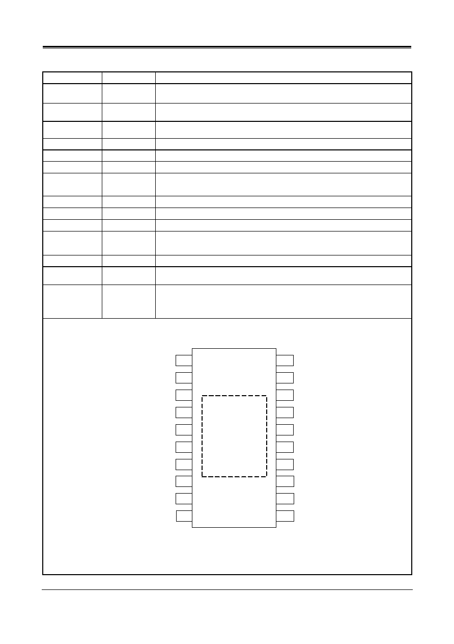
PIN CONFIGURATION
Symbol
Pin
Description
SD 1
SHUTDOWN places the entire device in shutdown mode when held high.
TTL compatible input.
+OUTA
3
Bridged-tied load positive output A.
-OUTA
5
Left channel output or bridged-tied load negative output A.
-INA
6
Negative input A.
+INA 8
Positive
input
A.
+INB 13
Positive
input
B.
BYPASS 14
BYPASS is a capacitor to the voltage divider for the internal mid-supply bias.
This terminal should be connected to a 0.1-F to 10-F capacitor C
B
.
B
-INB
15
Negative input B
-OUTB
16
Right channel output or bridged-tied load negative output B.
+OUTB
18
Bridged-tied load positive output B.
HP-IN 20
Headphone input detection.
A logical low sets BTL mode, a logical high sets SE mode.
VDD
4, 17
Supply voltage
GND
2, 9, 10
11, 12, 19
Ground
GND (SDPR)
7
Connected to ground, it is compatible for LM4863
SDPR: Shutdown Power Preparation.
Pop noise free in shutdown control, please refer to application information
TSSOP20
GND
16
17
18
19
20
2
3
4
1
GND
+OUTA
VDD
-OUTA
5
-INA
+OUTB
VDD
-OUTB
-INB
15
6
14
7
GND(SDPR)
SD
BYPASS
HP-IN
MS6863
13
+INA
8
GND
+INB
12
9
11
10
GND
GND
Thermal
Pad
GND
MO
SA
MS6863
Dual 2W Power Amplifiers with Stereo Headphone
REV 1 3
www.mosanalog.com
ORDERING INFORMATION
Package Part
number
Packaging Marking
Transport Media
20Pin TSSOP (lead free)
MS6863TGTR
MS6863G
2.5Units Tape and Reel
20Pin TSSOP (lead free)
MS6863TGU
MS6863G
75Units Tube
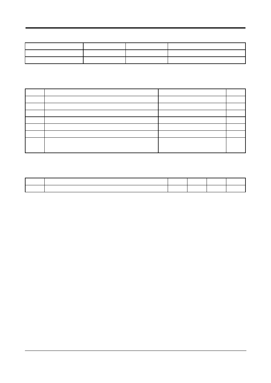
ABSOLUTE MAXIMUM RATINGS
Symbol
Parameter Rating
Unit
V
DD
Supply
voltage
6
V
V
ESD
Electrostatic handling
2000
V
T
STG
Storage temperature range
-65 to 150
T
A
Operating ambient temperature range
-40 to 85
T
J
Maximum junction temperature
150
T
S
Soldering temperature, 10 seconds
260
R
THJA
Thermal resistance from junction to ambient in free air
TSSOP20 (enhance thermal pad)
51
/W
OPERATING RATINGS
Symbol Parameter Min Typ Max Unit
V
DD
Supply
voltage
2.7 5 5.5 V
MO
SA
MS6863
Dual 2W Power Amplifiers with Stereo Headphone
REV 1 4
www.mosanalog.com
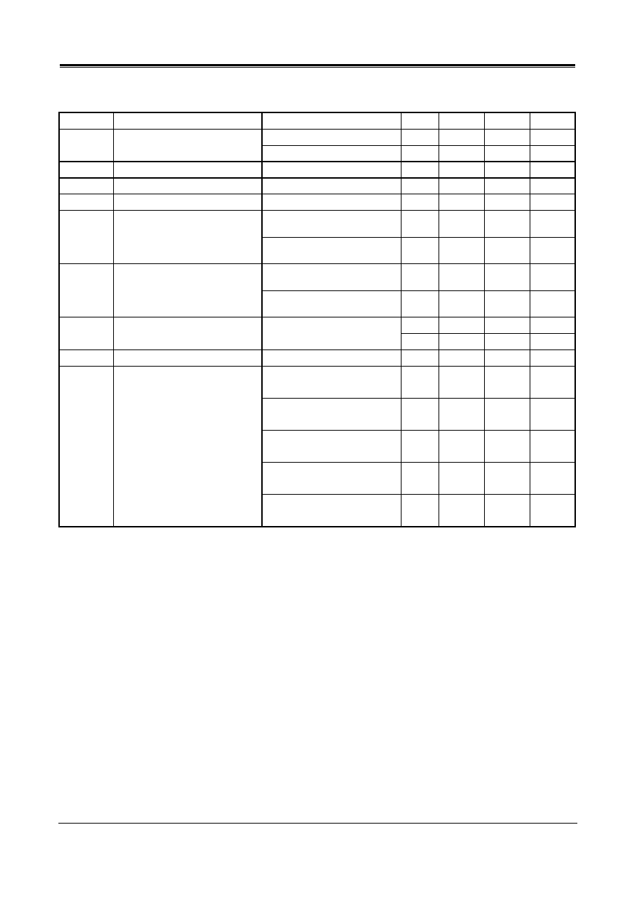
5V ELECTRICAL CHARACTERISTICS
Ta = 25∞C, V
DD
=5V, f=1kHz, BW<30kHz, unless otherwise specified.
Symbol Parameter
Conditions Min
Typ
Max
Unit
BTL Mode, V
IN
=0V, I
O
=0A - 5.9 - mA
I
Q
Quiescent current
SE Mode, V
IN
=0V, I
O
=0A - 3.1 - mA
I
SD
Shutdown current
SD Mode, V
SD
=V
DD
- 0.4 2 uA
V
SDH
Shutdown input voltage high
2.0
-
-
V
V
SDL
Shutdown input voltage low
-
-
0.8
V
BTL Mode, R
L
=8
Po=1W
- 95 - dB
CS Channel
separation
SE Mode, R
L
=32
Po=60mW
- 90 - dB
BTL Mode , R
L
=8
C
BP
=1uF, f=100Hz
- 63 - dB
PSRR
Power supply rejection ratio
SE Mode , R
L
=32
C
BP
=10uF, f=100Hz
- 55 - dB
- -75 -68 dB
THD+N
Total harmonic distortion plus
noise
SE mode, R
L
=32, 75mW
- 0.018 0.04 %
S/N
Signal-to-noise ratio
SE mode, A-weighting
90
95
-
dB
BTL Mode, R
L
= 3
THD+N = 1%
- 2.3 - W
BTL Mode, R
L
= 4
THD+N = 1%
- 2 - W
BTL Mode, R
L
= 8
THD+N = 1%
- 1.3 - W
SE Mode, R
L
=8
THD+N = 1%
- 300m - W
Po Output
power
SE Mode, R
L
= 32
THD+N = 1%
- 90m - W
MO
SA
MS6863
Dual 2W Power Amplifiers with Stereo Headphone
REV 1 5
www.mosanalog.com
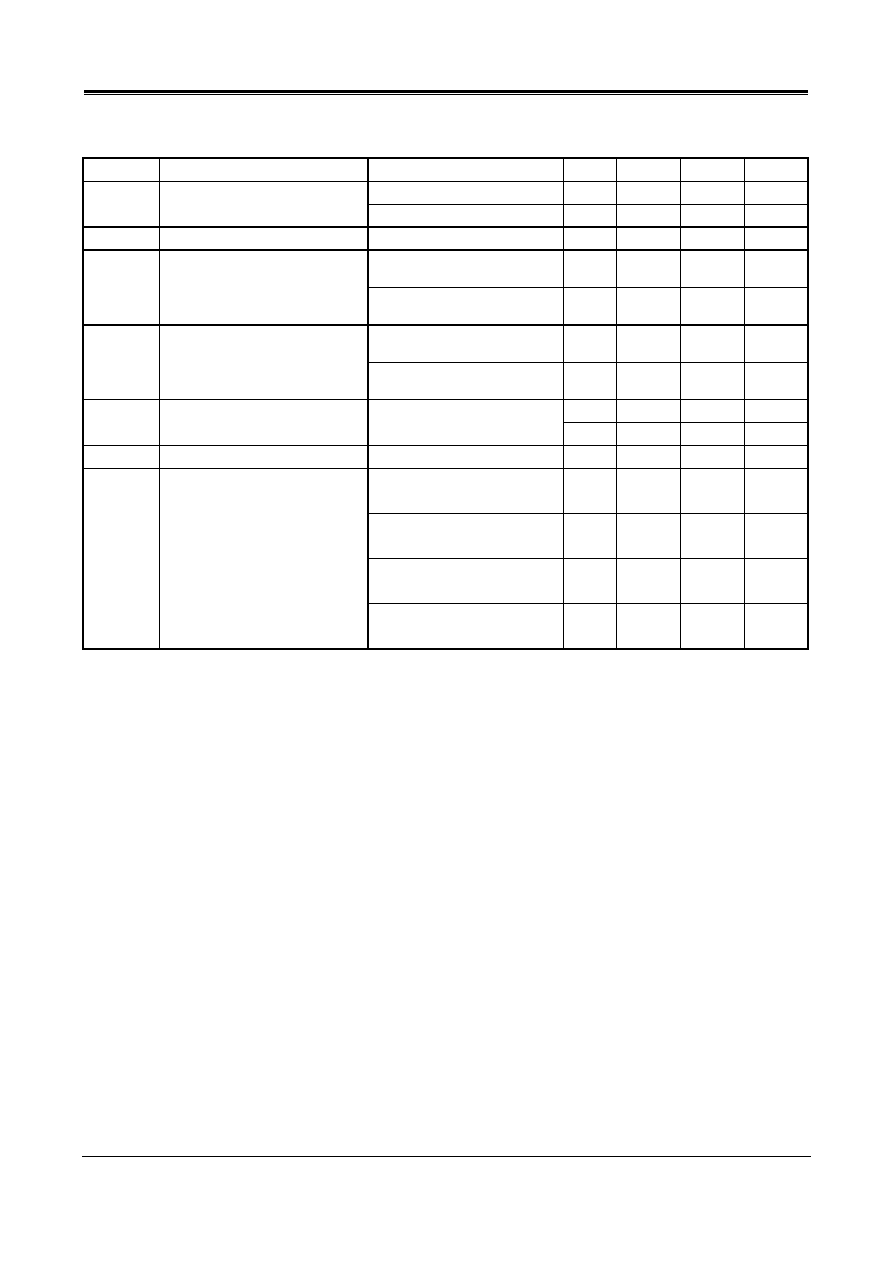
3.3 V ELECTRICAL CHARACTERISTICS
Ta = 25∞C, V
DD
=3.3V, f=1kHz, BW<30kHz, unless otherwise specified.
Symbol Parameter
Conditions Min
Typ
Max
Unit
BTL Mode, V
IN
=0V, I
O
=0A - 5.4 - mA
I
Q
Quiescent current
SE Mode, V
IN
=0V, I
O
=0A - 2.8 - mA
I
SD
Shutdown current
SD Mode, V
SD
=V
DD
- 0.2 - uA
BTL Mode, R
L
=8
Po=120mW
- 83 - dB
CS Channel
separation
SE Mode, R
L
=32
Po=25mW
- 86 - dB
BTL Mode , R
L
=8
C
BP
=1uF, f=100Hz
- 60 - dB
PSRR
Power supply rejection ratio
SE Mode , R
L
=32
C
BP
=10uF, f=100Hz
- 53 - dB
- -73 -65 dB
THD+N
Total harmonic distortion plus
noise
SE mode, R
L
=32, 25mW
0.022
0.056 %
S/N
Signal-to-noise ratio
SE mode, A-weighting
89
94
-
dB
BTL Mode, R
L
= 4
THD+N = 1%
- 0.8 - W
BTL Mode, R
L
= 8
THD+N = 1%
- 0.5 - W
SE Mode, R
L
=8
THD+N = 1%
- 130m - W
Po Output
power
SE Mode, R
L
= 32
THD+N = 1%
- 40m - W