
1
MS7200L/7201AL/7202AL
MOSEL VITELIC
MS7200L/01AL/02AL Rev. 1.0 January 1995
MS7200L/7201AL/7202AL
256 x 9, 512 x 9, 1K x 9
CMOS FIFO
Features
s
First-In/First-Out static RAM based dual port
memory
s
Three densities in a x9 configuration
s
Low power versions
s
Includes empty, full, and half full status flags
s
Direct replacement for industry standard
Mostek and IDT
s
Ultra high-speed 30 MHz FIFOs available with
33 ns cycle times.
s
Fully expandable in both depth and width
s
Simultaneous and asynchronous read and write
s
Auto retransmit capability
s
TTL compatible interface, single 5V � 10%
power supply
s
Available in 28 pin 300 mil and 600 mil plastic
DIP, 32 Pin PLCC and 330 mil SOG
Descriptions
The MS7200L/7201AL/7202AL are dual-port
static RAM based CMOS First-In/First-Out (FIFO)
memories organized in nine-bit wide words. The
devices are configured so that data is read out in
the same sequential order that it was written in.
Additional expansion logic is provided to allow for
unlimited expansion of both word size and depth.
The dual-port RAM array is internally sequenced
by independent Read and Write pointers with no
external addressing needed. Read and write
operations are fully asynchronous and may occur
simultaneously, even with the device operating at
full speed. Status flags are provided for full, empty,
and half-full conditions to eliminate data underflow
and overflow. The x9 architecture provides an
additional bit which may be used as a parity or
control bit. In addition, the devices offer a retransmit
capability which resets the Read pointer and allows
for retransmission from the beginning of the data.
The MS7200L/7201AL/7202AL are available in a
range of frequencies from 10 to 30 MHz (33 - 100 ns
cycle times). A low power version with a 500�A
power down supply current is available. They are
manufactured on Mosel-Vitelic's high performance
1.2� CMOS process and operate from a single 5V
power supply.
W
WRITE
CONTROL
WRITE
POINTER
READ
POINTER
READ
CONTROL
RESET
LOGIC
FLAG
LOGIC
EXPANSION
LOGIC
THREE
STATE
BUFFERS
DATA OUTPUTS (Q0-Q8)
DATA INPUTS (Q0-Q8)
R
XI
EF
HF
FF
XO
RS
FL / RT
RAM
ARRAY
256x9
512x9
1Kx9
Block Diagram
28-PIN PDIP
Pin Configurations
32-PIN PLCC
V
D6
D7
FL / RT
EF
XO / HF
CC
Q2
Q3
Q8
GND
Q1
Q0
FF
XI
D0
D1
D2
D3
D8
300 mil
600 mil
DIP
&
330 mil
SOG
W
Q6
Q5
Q4
R
Q7
RS
D5
D4
1
2
3
4
5
6
7
8
9
10
11
12
13
14
28
27
26
25
24
23
22
21
20
19
18
17
16
15
D
D
XI
FF
Q
Q
Q
D6
D7
NC
FL / RT
RS
EF
XO / HF
Q7
Q6
5
8
7
8
9
10
11
14
13
29
28
27
26
25
24
23
22
21
D
3
D
8
W
NC
V
CC
D
4
D
5
1
0
0
1
NC
2
14
Q
8
V
SS
NC
R
Q
4
Q
5
D2
Q
3
32 Pin PLCC
Top View
15 16 17 18 19 20
4
3
2
1 32 31 30

2
MS7200L/7201AL/7202AL
MOSEL VITELIC
MS7200L/01AL/02AL Rev. 1.0 January 1995
Signal Descriptions
INPUTS:
Data In (D
0
- D
8
)
These data inputs accept 9-bit data words for
sequential storage in the FIFO during write
operations.
CONTROLS:
Reset (
RS
)
The reset input is active LOW. When asserted,
the device is asynchronously reset, and both the
read and write internal pointers are set to the first
location in the FIFO. A Reset is required after
power-up before a write operation can occur. Both
Read Enable (
R
) and Write Enable (
W
) must be
HIGH during Reset.
Read Enable (
R
)
The read enable input is active LOW. As long as
the Empty Flag (
EF
) is not set, the read cycle is
started on the falling edge of this signal. The data is
accessed on a First-In/First-Out basis, independent
of any write activity, and is presented on the Data
Output pins (Q0 - Q8). When
R
goes HIGH the Data
Output pins return to the high impedance state, and
the read pointer is incremented. When the FIFO is
empty or all of the data has been read, the Empty
Flag will be set and further read operations are
inhibited until a valid write operation has been
performed.
Write Enable (
W
)
The write enable input is active LOW. As long as
the Full Flag (
FF
) is not set, the write cycle is started
on the falling edge of this signal. The data present
on the Data Input pins (D0 - D8) is stored
sequentially, independent of any read activity.
When
W
goes HIGH the write cycle is terminated
and the write pointer is incremented. When the
maximum capacity of the FIFO has been reached
the Full Flag will be set, and further write operations
are inhibited until a valid read operation has been
performed.
Expansion In (
XI
)
This input pin serves two purposes. When
grounded, it indicates that the device is being
operated in the single device mode. In Depth
Expansion mode, this pin is connected to the
Expansion Out Output (
XO
) of the previous device.
First Load/Retransmit (
FL
/
RT
)
This is a dual-purpose input. In single device
mode (when Expansion In (
XI
) is grounded) this pin
acts as the retransmit input. A LOW pulse on this
will reset the read pointer to the first memory
location of the FIFO. The write pointer is unaffected.
Both the read enable (
R
) and write enable (
W
)
inputs must remain HIGH during the retransmit
cycle.
In Depth Expansion mode this pin acts as a first
load indicator. It must be grounded on the first
device in the chain to indicate which device is the
first to receive data.
OUTPUTS:
Data Output (Q
0
- Q
8
)
A 9 bit data word from the FIFO is output on these
pins during read operations. They are in the high
impedance state whenever
R
is HIGH.
Empty Flag (
EF
)
This output is active LOW. When all of the data
has been read from the FIFO (defined as when the
Read pointer is one location behind the Write
pointer) this flag will be set. The Data Output pins
will be forced into the high impedance state, and all
further read operations will be inhibited until a valid
write operation has been performed (which will
reset this flag).
Full Flag (
FF
)
This output is active LOW. To prevent data
overflow, when the maximum capacity of the FIFO
has been reached (defined as when the Write
pointer is one location behind the Read pointer) this
flag will be set. All further write operations will be
inhibited until a valid read operation has been
performed (which will reset this flag).
Expansion Out/Half Full Flag (
XO
/
HF
)
This dual-purpose output is active LOW. In single
device mode (when Expansion In (
XI
) is grounded)
this flag will be set at the falling edge of the next
write operation after the FIFO has reached one-half
of its maximum capacity. This flag will remain set as
long as the difference between the read pointer and
the write pointer is greater than one-half of the
maximum capacity of the FIFO.
In Depth Expansion mode, this output is
connected to the Expansion In Input of the next
device in the chain. The Expansion Out pin
provides a pulse to the next device in the chain
when the last memory location has been reached.
3
MS7200L/7201AL/7202AL
MOSEL VITELIC
MS7200L/01AL/02AL Rev. 1.0 January 1995
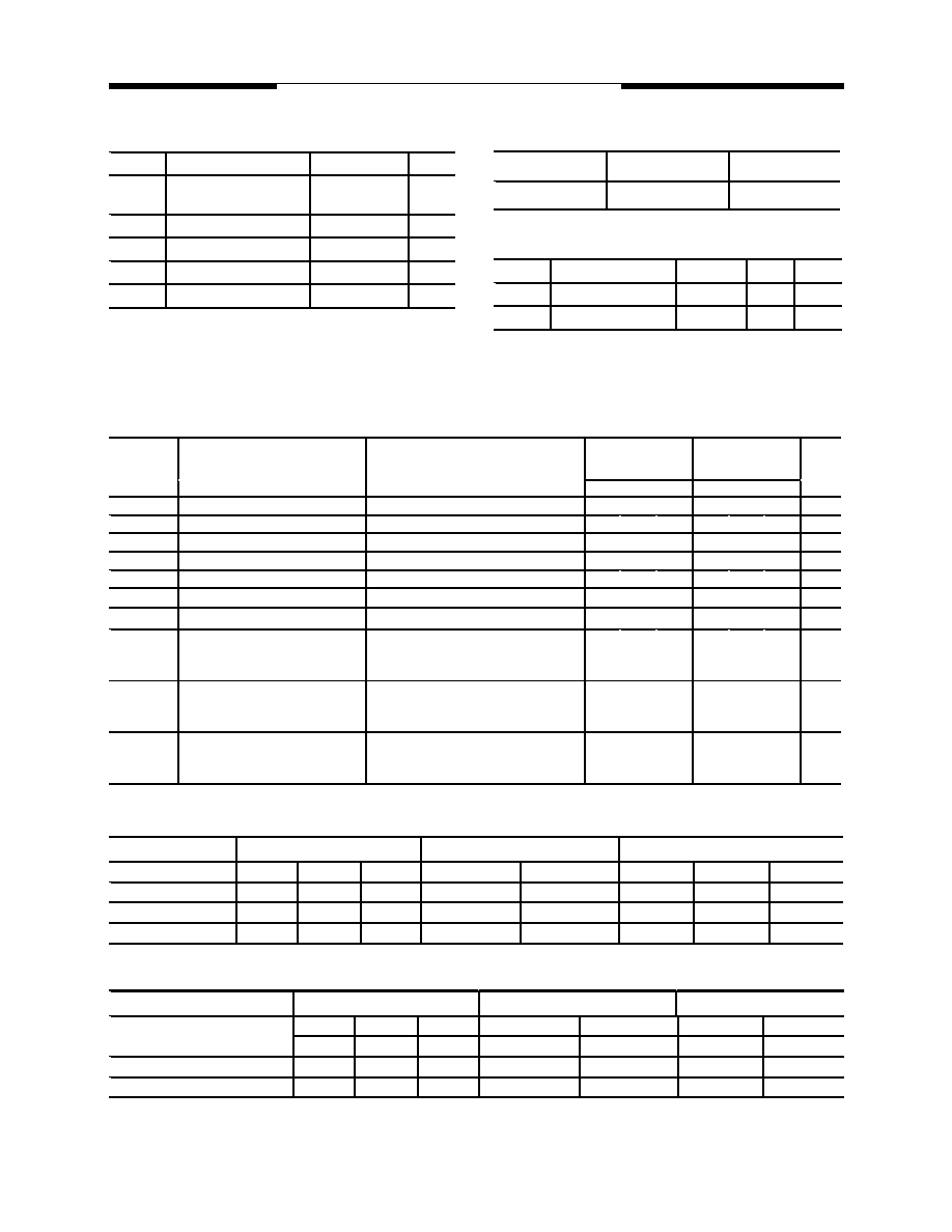
Operating Range
Capacitance
(1)
T
A
= 25�C, f = 1.0MHz
Range
Ambient
Temperature
Vcc
Commercial
0
�
C to + 70
�
C
5V
�
10%
Symbol
Parameter
Condition
Unit
V
TERM
Terminal Voltage with
Repect to GND
-0.5 to +7.0
V
T
BIAS
Temperature Under Bias
-10 to +125
�
C
T
STG
Storage Temperature
-60 to +150
�
C
P
T
Power Dissipation
1.0
W
I
OUT
DC Output Current
20
mA
Absolute Maximum Ratings
(1)
Symbol
Parameter
Condition
Max.
Unit
C
IN
Input Capacitance
V
IN
= 0V
4
pF
C
Q
Output Capacitance
V
DQ
= 0V
6
pF
DC Electrical Characteristics (over the commercial operating range)
Depth Expansion/Compound Expansion Mode
NOTE:
1.
XI
is connected to
XO
of previous device. See Figure 15.
RS
= Reset Input.
FL
/
RT
= First Load/Retransmit.
EF
= Empty Flag
Output.
FF
Full Flag Output.
XI
= Expansion Input.
1.
Stresses greater than those listed under ABSOLUTE
MAXIMUM RATINGS may cause permanent damage to the
device. This is a stress rating only and functional operation
of the device at these or any other conditions above those
indicated in the operational sections of this specification is
not implied. Exposure to absolute maximum rating conditions
for extended periods may affect reliability.
Truth Tables
Single Device Configuration/Width Expansion Mode
NOTE: 1. Pointer will increment if flag is high.
Mode
Inputs
Internal Status
Outputs
RS
RT
XI
Read Pointer
Write Pointer
EF
FF
HF
Reset
0
X
0
Location Zero
Location Zero
0
1
1
Retransmit
1
0
0
Location Zero
Unchanged
X
X
X
Read/Write
1
1
0
Increment
(1)
Increment
(1)
X
X
X
Mode
Inputs
Internal Status
Outputs
RS
FL
XI
Read Pointer
Write Pointer
EF
FF
Reset-First Device
0
0
(1)
Location Zero
Location Zero
0
1
Reset all Other Devices
0
1
(1)
Location Zero
Unchanged
0
1
Read/Write
1
X
(1)
X
X
X
X
Test
MS7200L/7201AL
7202AL
(-25, -35)
MS7200L/7201AL
7202AL
(-50, -80)
Parameter
Parameter
Test Conditions
Min. Typ. Max. Min.
Typ. Max. Units
V
IL
Input Low Voltage
-
-
0.8
-
-
0.8
V
V
IH
Input High Voltage
2.0
-
-
2.0
-
-
V
I
IL
Input Leakage Current
V
CC
= Max, V
IN
= 0Vto V
CC
-1
1
-1
1
�
A
I
OL
Output Leakage Current
V
CC
= Max, R= V
IH
, V
IN
= 0V toV
CC
-10
10
-10
10
�
A
V
OL
Output Low Voltage
V
CC
= Min, I
OL
= 8mA
-
-
0.4
-
-
0.4
V
V
OH
Output High Voltage
V
CC
= Min, I
OH
= -2mA
2.4
-
-
2.4
-
-
V
I
CC1
Operating Power Supply Current V
CC
= Max, I
I/O
= 0mA, F = F
m ax
-
-
125
-
50
80
mA
I
CC2
Average Standby Current
V
CC
= Max,
R
=
W
=
RS
=
FL
/
RT
=
V
IH
,
I
I/O
= 0mA
-
-
15
-
5
8
mA
I
CCSB(S)
Power Down Power Supply
Current (Standard Power)
V
CC
= Max,
R
=
W
=
RS
=
FL
/
RT
>
V
CC
-0.2V, V
IN
> V
CC
-0.2V or V
IN
<
0.2V
-
-
5
-
-
5
mA
I
CCSB(L)
Power Down Power Supply
Current (Low Power)
V
CC
= Max,
R
=
W
=
RS
=
FL
/
RT
>
V
CC
-0.2V, V
IN
> V
CC
-0.2V or V
IN
<
0.2V
-
-
500
-
-
500
�
A

4
MS7200L/7201AL/7202AL
MOSEL VITELIC
MS7200L/01AL/02AL Rev. 1.0 January 1995
AC Electrical Characteristics (over the commercial operating range)
Parameter
MS7200L-25
MS7201AL-25
MS7202AL-25
MS7200L-35
MS7201AL-35
MS7202AL-35
MS7200L-50
MS7201AL-50
MS7202AL-50
MS7200L-80
MS7201AL-80
MS7202AL-80
Name
Parameter
Min.
Max.
Min.
Max.
Min.
Max.
Min.
Max.
Units
S
Shift Frequency
--
30
--
22.2
--
15
--
10
MHz
Read Cycle
t
RC
Read Cycle Time
33
--
45
--
65
--
100
--
ns
t
A
Access Time
--
25
--
35
--
50
--
80
ns
t
RPW
Read Pulse Width
25
--
35
--
50
--
80
--
ns
t
RR
Read Recovery Time
8
--
10
--
15
--
20
--
ns
t
RLZ
(2)
Read Pulse Low to Data Bus at Low Z
5
--
5
--
10
--
10
--
ns
t
RHZ
(2,3)
Read Pulse High to Data Bus at High Z
--
18
--
20
--
30
--
30
ns
t
DV
Data Valid from Read Pulse High
5
--
5
--
5
--
5
--
ns
Write Cycle
t
WC
Write Cycle Time
33
--
45
--
65
--
100
--
ns
t
WPW
(1)
Write Pulse Width
25
--
35
--
50
--
80
--
ns
t
WR
Write Recovery Time
8
--
10
--
15
--
20
--
ns
t
DS
Data Setup Time
15
--
18
--
30
--
40
--
ns
t
DH
Data Hold Time
0
--
0
--
5
--
10
--
ns
t
WLZ
(2,3)
Write Pulse High to Data Bus at Low Z
5
--
10
--
15
--
20
--
ns
Flag Timing
t
REF
Read Low to Empty Flag Low
--
25
--
30
--
45
--
60
ns
t
RHF
Read High to Half Full Flag High
--
33
--
45
--
65
--
100
ns
t
RFF
Read High to Full Flag High
--
25
--
30
--
45
--
60
ns
t
WEF
Write High to Empty Flag High
--
25
--
30
--
45
--
60
ns
t
WFF
Write Low to Full Flag Low
--
25
--
30
--
45
--
60
ns
t
WHF
Write Low to Half Full Flag Low
--
33
--
45
--
65
--
100
ns
t
RPE
Read Pulse Width After EF High
25
--
35
--
50
--
80
--
ns
t
WPF
Write Pulse Width After
FF
High
25
--
35
--
50
--
80
--
ns
Reset Timing
t
RSC
Reset Cycle Time
33
--
45
--
65
--
100
--
ns
t
RS
(1)
Reset Pulse Width
25
--
35
--
50
--
80
--
ns
t
RSS
Reset Set Up Time
25
--
35
--
50
--
80
--
ns
t
RSR
Reset Recovery Time
8
--
10
--
15
--
20
--
ns
t
EFL
Reset to Empty Flag Low
--
33
--
45
--
65
--
100
ns
t
HFH
Reset to Half Full Flag High
--
33
--
45
--
65
--
100
ns
t
FFH
Reset to Full Flag High
--
33
--
45
--
65
--
100
ns
Retransmit Timing
t
RTC
Retransmit Cycle Time
33
--
45
--
65
--
100
--
ns
t
RT
(1)
Retransmit Pulse Width
25
--
35
--
50
--
80
--
ns
t
RTS
Retransmit Set up Time
25
--
35
--
50
--
80
--
ns
t
RTR
Retransmit Recovery Time
8
--
10
--
15
--
20
--
ns
Expansion Timing
t
XOL
Read/Write to
XO
Low
--
25
--
35
--
50
--
80
ns
t
XOH
Read/Write to
XO
High
--
25
--
35
--
50
--
80
ns
t
XI
XI
Pulse Width
25
--
35
--
50
--
80
--
ns
t
XIS
XI
Set up Time
15
--
15
--
15
--
15
--
ns
t
XIR
XI
Recovery Time
8
--
10
--
10
--
10
--
ns
NOTES:
1.
Pulse widths less than minimum value are not allowed.
2.
Values guaranteed by design, not currently tested.
3.
Only applies to read data flow-through mode.

5
MS7200L/7201AL/7202AL
MOSEL VITELIC
MS7200L/01AL/02AL Rev. 1.0 January 1995
INCLUDING
JIG AND
SCOPE
Figure 1a
30pF
R2
255
R1 480
5V
OUTPUT
INCLUDING
JIG AND
SCOPE
5pF
R2
255
R1 480
5V
OUTPUT
Figure 1b
167
OUTPUT
THEVENIN EQUIVALENT
Equivalent to:
ALL INPUT PULSES
90%
90%
10%
10%
5 ns
5 ns
GND
3.0V
1.73V
Figure 2
AC Test Conditions
Key to Switching Waveforms
WAVEFORM
INPUTS
OUTPUTS
MUST BE
STEADY
WILL BE
STEADY
MAY CHANGE
FROM H TO L
WILL BE
CHANGING
FROM H TO L
MAY CHANGE
FROM L TO H
WILL BE
CHANGING
FROM L TO H
DON'T CARE:
ANY CHANGE
PERMITTED
CHANGING:
STATE
UNKNOWN
DOES NOT
APPLY
CENTER
LINE IS HIGH
IMPEDANCE
"OFF" STATE
AC Test Loads and Waveforms
Timing Waveforms
Input Pulse Levels
0V~ 3.0V
Input Rise and Fall Times
5 ns
Timing Reference Level
1.5V
RS
t
RS
t
RSS
t
RSC
t
EFL
t
RSR
t
HFH
, t
FFH
t
RSS
W
EF
HF, FF
R
RESET
Q0-Q8
t
RC
t
A
t
RPW
t
RR
t
RLZ
t
DV
t
RHZ
t
A
READ
DATA VALID
READ
DATA VALID
R
ASYNCHRONOUS READ OPERATION