MOSEL VITELIC
1
V54C316162VA
HIGH PERFORMANCE
3.3 VOLT 1M X 16 SYNCHRONOUS DRAM
2 BANKS X 512Kbit X 16
V54C316162VA Rev. 1.0 January 1998
PRELIMINARY
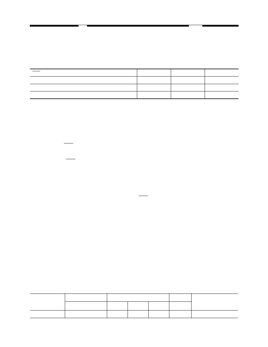
CAS Latency = 3
8
10
12
System Frequency (f
CK
)
125 MHz
100 MHz
83 MHz
Clock Cycle Time (t
CK3
)
8 ns
10 ns
12 ns
Clock Access Time (t
AC3
)
7 ns
8 ns
9 ns
Features
s
2 banks x 512Kbit x 16 organization
s
High speed data transfer rates up to 125 MHz
s
Full Synchronous Dynamic RAM, with all signals
referenced to clock rising edge
s
Single Pulsed RAS Interface
s
Dual Data Mask for Byte Control
s
Dual Banks controlled by A11
s
Programmable CAS Latency: 1, 2, 3
s
Programmable Wrap Sequence: Sequential or
Interleave
s
Programmable Burst Length:
1, 2, 4, 8 and full page for Sequential Type
1, 2, 4, 8 for Interleave Type
s
Multiple Burst Read with Single Write Operation
s
Automatic and Controlled Precharge Command
s
Random Column Address every CLK (1-N Rule)
s
Suspend Mode and Power Down Mode
s
Auto Refresh and Self Refresh
s
Refresh Interval: 4096 cycles/64 ms
s
Available in 50 Pin 400 mil TSOP-II
s
LVTTL Interface
s
Single +3.3 V
�
0.3 V Power Supply
Description
The V54C316162VA is a dual bank Synchronous
DRAM organized as 2 banks x 512Kbit x 16. The
V54C316162VA achieves high speed data transfer
rates up to 125 MHz by employing a chip architec-
ture that prefetches multiple bits and then synchro-
nizes the output data to a system clock
All of the control, address, data input and output
circuits are synchronized with the positive edge of
an externally supplied clock.
Operating the two memory banks in an inter-
leaved fashion allows random access operation to
occur at higher rate than is possible with standard
DRAMs. A sequential and gapless data rate of up to
125 MHz is possible depending on burst length,
CAS latency and speed grade of the device.
Device Usage Chart
Operating
Temperature
Range
Package Outline
Access Time (ns)
Power
Temperature
Mark
T
8
10
12
Std.
0
�
C to 70
�
C
�
�
�
�
�
Blank

2
V54C316162VA Rev. 1.0 January 1998
MOSEL VITELIC
V54C316162VA
C = CMOS PROCESS
SYCHRONOUS
DRAM FAMILY
REVISION
LEVEL
DEVICE
NUMBER
MOSEL-VITELIC
MANUFACTURED
2 BANKS x 512Kbit x 16 (4K REFRESH)
PKG
SPEED
V
54
C
31
62
T
3.3V, LVTTL, INTERFACE
T = TSOP-II
31161602-01
61
8 ns
10 ns
12 ns
PWR.
BLANK (NORMAL)
50 Pin Plastic TSOP-II
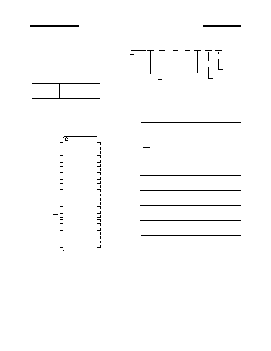
PIN CONFIGURATION
Top View
Pin Names
V
CC
I/O
1
I/O
2
V
SSQ
I/O
3
I/O
4
V
CCQ
I/O
5
I/O
6
V
SSQ
I/O
7
I/O
8
V
CCQ
LDQM
WE
CAS
RAS
CS
A
11
A
10
A
0
A
1
A
2
A
3
V
CC
V
SS
I/O
16
I/O
15
V
SSQ
I/O
14
I/O
13
V
CCQ
I/O
12
I/O
11
V
SSQ
I/O
10
I/O
9
V
CCQ
NC
UDQM
CLK
CKE
NC
A
9
A
8
A
7
A
6
A
5
A
4
V
SS
1
2
3
4
5
6
7
8
9
10
11
12
13
14
15
16
17
18
19
20
21
22
23
24
25
50
49
48
47
46
45
44
43
42
41
40
39
38
37
36
35
34
33
32
31
30
29
28
27
26
31161600 02
CLK
Clock Input
CKE
Clock Enable
CS
Chip Select
RAS
Row Address Strobe
CAS
Column Address Strobe
WE
Write Enable
A
0
�A
10
Address Inputs
A
11
(BS)
Bank Select
I/O
1
�I/O
16
Data Input/Output
DQM, LDQM, UDQM
Data Mask
V
CC
Power (+3.3V)
V
SS
Ground
V
CCQ
Power for I/O's (+3.3V)
V
SSQ
Ground for I/O's
NC
Not connected
Description
Pkg.
Pin Count
TSOP-II
T
50

MOSEL VITELIC
V54C316162VA
3
V54C316162VA Rev. 1.0 January 1998
Absolute Maximum Ratings*
Ambient Temperature
Under Bias ................................... �10
�
C to +80
�
C
Storage Temperature (plastic) ......... -55 to +125
�
C
Input/Output Voltage... -0.5 to Min (V
CC
+0.5, 4.6) V
Voltage Relative to V
SS
.................. -1.0V to +4.6 V
Data Output Current ..................................... 50 mA
Power dissipation .......................................... 1.0 W
*
Note:
Operation above Absolute Maximum Ratings can
adversely affect device reliability.
Capacitance*
T
A
= 0 to 70
�
C, V
CC
= 3.3 V
�
0.3 V, f = 1 Mhz
*
Note:
Capacitance is sampled and not 100% tested.
Symbol
Parameter
Max. Unit
C
I1
Input Capacitance (A0 to A11)
4
pF
C
I2
Input Capacitance
RAS, CAS, WE, CS, CLK, CKE, DQM
4
pF
C
IO
Output Capacitance (I/O)
5
pF
Block Diagram
I/O1
Data Latches
Data Latches
8
16
Column Decoder and DQ Gate
Sense Amplifiers
Data Input/Output Buff
ers
16
CKE Buffer
CLK Buffer
CS Buffer
RAS Buffer
CAS Buffer
WE Buffer
DQM Buffer
CKE
CLK
CS
RAS
CAS
DQM
WE
Command Decoder
Mode Register
Refresh Clock
Row
Address
Counter
Self
A1
A2
A3
A4
A5
A6
A7
A10
A8
A9
A0
A11 (BS)
12
12
Sequential
Control
Bank A
Row/Column
Select
Bank A
Predecode A
Column Decoder and I/O Gate
Sense Amplifiers
Sequential
Control
Bank B
Predecode B
16
Address Buff
ers (12)
Row/Column
Select
Bank B
3
11
3
11
11
Data Latches
16
Column Decoder and I/O Gate
Sense Amplifiers
256
Memory Bank B
2048 x 1024
Memory Bank B
2048 x 256
2048
Ro
w Decoder
Ro
w Decoder
16
16
16
16
16
16
16
1024
256
Memory Bank A
2048 x 256
2048
Ro
w Decoder
Ro
w Decoder
I/O2
I/O3
I/O4
I/O5
I/O6
I/O7
I/O16

4
V54C316162VA Rev. 1.0 January 1998
MOSEL VITELIC
V54C316162VA
Signal Pin Description
Pin
Type
Signal
Polarity
Function
CLK
Input
Pulse
Positive
Edge
The system clock input. All of the SDRAM inputs are sampled on the rising edge of the
clock.
CKE
Input
Level
Active High Activates the CLK signal when high and deactivates the CLK signal when low, thereby
inititiates either the Power Down mode, Suspend mode or the Self Refresh mode.
CS
Input
Pulse
Active Low
CS enables the command decoder when low and disables the command decoder
when high. When the command decoder is disabled, new commands are ignored but
previous operations continue.
RAS, CAS
WE
Input
Pulse
Active Low
When sampled at the positive rising edge of the clock, CAS, RAS, and WE define the
command to be executed by the SDRAM.
A
0
�A
10
Input
Level
--
During a Bank Activate command cycle, A0-A10 defines the row address (RA0-RA10)
when sampled at the rising clock edge.
During a Read or Write command cycle, A0-A9 defines the column address
(CA0-CAn) when sampled at the rising clock edge.CAn depends from the SDRAM
organization.
1M x 16 SDRAM CAn = CA7
In addition to the column address, A10 is used to invoke autoprecharge operation at
the end of the burst read or write cycle. If A10 is high, autoprecharge is selected and
A11 defines the bank to be precharged (low=bank A, high=bank B). If A10 is low,
autoprecharge is disabled.
During a Precharge command cycle, A10 is used in conjunction with A11 to control
which bank(s) to precharge. If A10 is high, both bank A and bank B will be precharged
regardless of the state of A11. If A10 is low, then A11 is used to define which bank to
precharge.
A
11
(BS)
Input
Level
--
Selects which bank is to be active. A11 low selects bank A and A11 high selects bank
B.
I/O
1
�I/O
16
Input
Output
Level
--
Data Input/Output pins operate in the same manner as on conventional DRAMs.
DQM
LDQM
UDQM
Input
Pulse
Active High The Data Input/Output mask places the I/O buffers in a high impedance state when
sampled high. In Read mode, DQM has a latency of two clock cycles and controls the
output buffers like an output enable. In Write mode, DQM has a latency of zero and
operates as a word mask by allowing input data to be written if it is low but blocks the
write operation if DQM is high.
V
CC
, V
SS
Supply
Power and ground for the input buffers and the core logic.
V
CCQ
, V
SSQ
Supply
--
--
Isolated power supply and ground for the output buffers to provide improved noise
immunity.

5
V54C316162VA Rev. 1.0 January 1998
MOSEL VITELIC
V54C316162VA
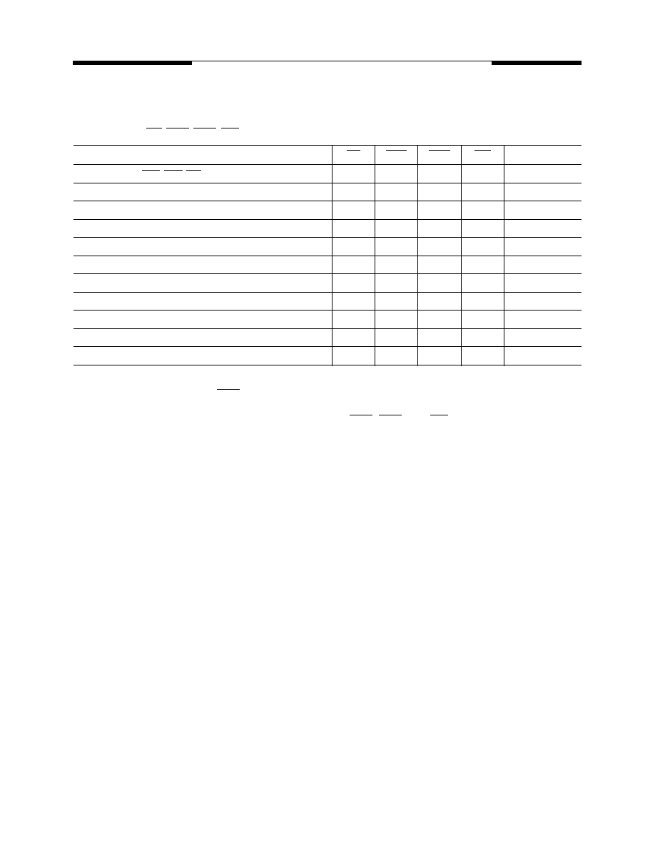
Operation Definition
All of SDRAM operations are defined by states of
control signals CS, RAS, CAS, WE, and DQM at the
positive edge of the clock. The following list shows
the most important operation commands.
Mode Register
For application flexibility, a CAS latency, a burst
length, and a burst sequence can be programmed in
the SDRAM mode register. The mode set operation
must be done before any activate command after
the initial power up. Any content of the mode register
can be altered by re-executing the mode set com-
mand. Both banks must be in precharged state and
CKE must be high at least one clock before the
mode set operation. After the mode register is set, a
Standby or NOP command is required. Low signals
of RAS, CAS, and WE at the positive edge of the
clock activate the mode set operation. Address input
data at this timing defines parameters to be set as
shown in the following table.
Operation
CS
RAS
CAS
WE
(L/U)DQM
Standby, Ignore RAS, CAS, WE and Address
H
X
X
X
X
Row Address Strobe and Activating a Bank
L
L
H
H
X
Column Address Strobe and Read Command
L
H
L
H
X
Column Address Strobe and Write Command
L
H
L
L
X
Precharge Command
L
L
H
L
X
Burst Stop Command
L
H
H
L
X
Self Refresh Entry
L
L
L
H
X
Mode Register Set Command
L
L
L
L
X
Write Enable/Output Enable
X
X
X
X
L
Write Inhibit/Output Disable
X
X
X
X
H
No Operation (NOP)
L
H
H
H
X
