
MOSEL VITELIC
1
V54C365404VC
HIGH PERFORMANCE 143/133/125 MHz
3.3 VOLT 16M X 4 SYNCHRONOUS DRAM
4 BANKS X 4Mbit X 4
V54C365404VC Rev. 0.6 September 1999
PRELIMINARY
7
75
8PC
8
System Frequency (f
CK
)
143 MHz
133 MHz
125 MHz
125 MHz
Clock Cycle Time (t
CK3
)
7 ns
7.5 ns
8 ns
8 ns
Clock Access Time (t
AC3
) CAS Latency = 3
5.4 ns
5.4 ns
6 ns
7 ns
Clock Access Time (t
AC2
) CAS Latency = 2
5.5 ns
6 ns
6 ns
7 ns
Features
s
4 banks x 4Mbit x 4 organization
s
High speed data transfer rates up to 143 MHz
s
Full Synchronous Dynamic RAM, with all signals
referenced to clock rising edge
s
Single Pulsed RAS Interface
s
Data Mask for Read/Write Control
s
Four Banks controlled by BA0 & BA1
s
Programmable CAS Latency: 2, 3
s
Programmable Wrap Sequence: Sequential or
Interleave
s
Programmable Burst Length:
1, 2, 4, 8 and full page for Sequential Type
1, 2, 4, 8 for Interleave Type
s
Multiple Burst Read with Single Write Operation
s
Automatic and Controlled Precharge Command
s
Random Column Address every CLK (1-N Rule)
s
Suspend Mode and Power Down Mode
s
Auto Refresh and Self Refresh
s
Refresh Interval: 4096 cycles/64 ms
s
Available in 54 Pin 400 mil TSOP-II
s
LVTTL Interface
s
Single +3.3 V
�
0.3 V Power Supply
Description
The V54C365404VC is a four bank Synchronous
DRAM organized as 4 banks x 4Mbit x 4. The
V54C365404VC achieves high speed data transfer
rates up to 143 MHz by employing a chip architec-
ture that prefetches multiple bits and then synchro-
nizes the output data to a system clock
All of the control, address, data input and output
circuits are synchronized with the positive edge of
an externally supplied clock.
Operating the four memory banks in an inter-
leaved fashion allows random access operation to
occur at higher rate than is possible with standard
DRAMs. A sequential and gapless data rate of up to
143 MHz is possible depending on burst length,
CAS latency and speed grade of the device.
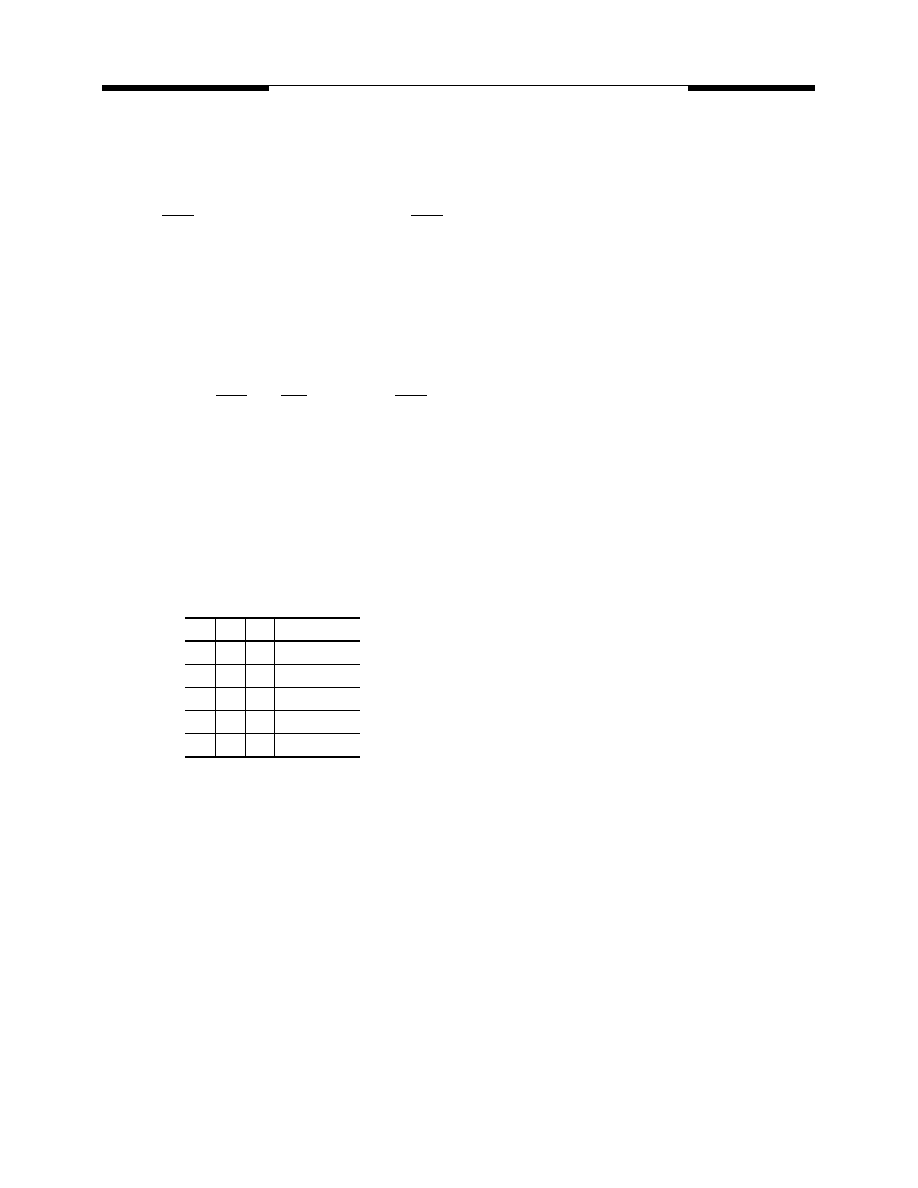
Device Usage Chart
Operating
Temperature
Range
Package Outline
Access Time (ns)
Power
Temperature
Mark
T
7
75
8PC
8
Std.
L
0
�
C to 70
�
C
�
�
�
�
�
�
�
Blank
2
V54C365404VC Rev. 0.6 September 1999
MOSEL VITELIC
V54C365404VC
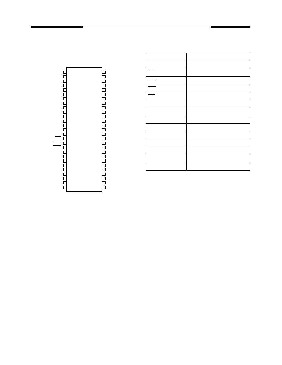
54 Pin Plastic TSOP-II
PIN CONFIGURATION
Top View
Pin Names
V
CC
NC
V
CCQ
NC
I/O
1
V
SSQ
NC
NC
V
CCQ
NC
I/O
2
V
SSQ
NC
V
CC
NC
WE
CAS
RAS
CS
BA0
BA1
A
10
A
0
A
1
A
2
A
3
V
CC
V
SS
NC
V
SSQ
NC
I/O
4
V
CCQ
NC
NC
V
SSQ
NC
I/O
3
V
CCQ
NC
V
SS
NC
DQM
CLK
CKE
NC
A
11
A
9
A
8
A
7
A
6
A
5
A
4
V
SS
1
2
3
4
5
6
7
8
9
10
11
12
13
14
15
16
17
18
19
20
21
22
23
24
25
26
27
54
53
52
51
50
49
48
47
46
45
44
43
42
41
40
39
38
37
36
35
34
33
32
31
30
29
28
31644002 02
CLK
Clock Input
CKE
Clock Enable
CS
Chip Select
RAS
Row Address Strobe
CAS
Column Address Strobe
WE
Write Enable
A
0
�A
11
Address Inputs
BA0, BA1
Bank Select
I/O
1
�I/O
4
Data Input/Output
DQM
Data Mask
V
CC
Power (+3.3V)
V
SS
Ground
V
CCQ
Power for I/O's (+3.3V)
V
SSQ
Ground for I/O's
NC
Not connected

MOSEL VITELIC
V54C365404VC
3
V54C365404VC Rev. 0.6 September 1999
Capacitance*
T
A
= 0 to 70
�
C, V
CC
= 3.3 V
�
0.3 V, f = 1 Mhz
*
Note:
Capacitance is sampled and not 100% tested.
Absolute Maximum Ratings*
Operating temperature range ................... 0 to 70
�
C
Storage temperature range .................-55 to 150
�
C
Input/output voltage.................. -0.3 to (V
CC
+0.3) V
Power supply voltage .......................... -0.3 to 4.6 V
Power dissipation ..............................................1 W
Data out current (short circuit).......................50 mA
*Note:
Stresses above those listed under "Absolute Maximum
Ratings" may cause permanent damage of the device.
Exposure to absolute maximum rating conditions for
extended periods may affect device reliability.
Symbol
Parameter
Max. Unit
C
I1
Input Capacitance (A0 to A11)
5
pF
C
I2
Input Capacitance
RAS, CAS, WE, CS, CLK, CKE, DQM
5
pF
C
IO
Output Capacitance (I/O)
6.5
pF
C
CLK
Input Capacitance (CLK)
4
pF
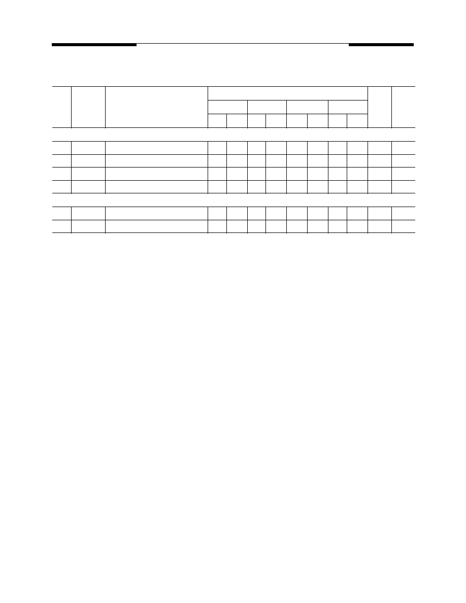
Block Diagram
Row decoder
Memory array
Bank 0
4096 x 1024
x 4 bit
Column decoder
Sense amplifi
er & I(O) b
u
s
Row decoder
Memory array
Bank 1
4096 x 1024
x 4 bit
Column decoder
Sense amplifi
er & I(O) b
u
s
Row decoder
Memory array
Bank 2
4096 x 1024
x 4 bit
Column decoder
Sense amplifi
er & I(O) b
u
s
Row decoder
Memory array
Bank 3
4096 x 1024
x 4 bit
Column decoder
Sense amplifi
er & I(O) b
u
s
Input buffer
Output buffer
I/O
1
-I/O
4
Column address
counter
Column address
buffer
Row address
buffer
Refresh Counter
A0 - A11, BA0, BA1
A0 - A9, AP, BA0, BA1
Control logic & timing generator
CLK
CKE
CS
RAS
CAS
WE
DQM
Row Addresses
Column Addresses

4
V54C365404VC Rev. 0.6 September 1999
MOSEL VITELIC
V54C365404VC
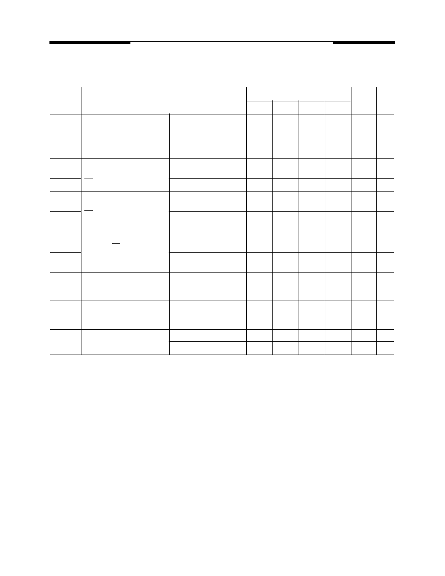
Signal Pin Description
Pin
Type
Signal
Polarity
Function
CLK
Input
Pulse
Positive
Edge
The system clock input. All of the SDRAM inputs are sampled on the rising edge of the
clock.
CKE
Input
Level
Active High Activates the CLK signal when high and deactivates the CLK signal when low, thereby
initiates either the Power Down mode, Suspend mode, or the Self Refresh mode.
CS
Input
Pulse
Active Low CS enables the command decoder when low and disables the command decoder when
high. When the command decoder is disabled, new commands are ignored but previous
operations continue.
RAS, CAS
WE
Input
Pulse
Active Low When sampled at the positive rising edge of the clock, CAS, RAS, and WE define the
command to be executed by the SDRAM.
A0 - A11
Input
Level
--
During a Bank Activate command cycle, A0-A11 defines the row address (RA0-RA11)
when sampled at the rising clock edge.
During a Read or Write command cycle, A0-An defines the column address (CA0-CAn)
when sampled at the rising clock edge.CAn depends from the SDRAM organisation:
16M x 4 SDRAM CAn = CA9 (Page Length = 1024 bits)
In addition to the column address, A10(=AP) is used to invoke autoprecharge operation
at the end of the burst read or write cycle. If A10 is high, autoprecharge is selected and
BA0, BA1 defines the bank to be precharged. If A10 is low, autoprecharge is disabled.
During a Precharge command cycle, A10(=AP) is used in conjunction with BA0 and BA1
to control which bank(s) to precharge. If A10 is high, all four banks will BA0 and BA1 are
used to define which bank to precharge.
BA0,
BA1
Input
Level
--
Selects which bank is to be active.
DQx
Input
Output
Level
--
Data Input/Output pins operate in the same manner as on conventional DRAMs.
DQM
Input
Pulse
Active High The Data Input/Output mask places the DQ buffers in a high impedance state when sam-
pled high. In Read mode, DQM has a latency of two clock cycles and controls the output
buffers like an output enable. In Write mode, DQM has a latency of zero and operates as
a word mask by allowing input data to be written if it is low but blocks the write operation
if DQM is high.
One DQM input it present in x4 SDRAMs.
VCC, VSS
Supply
Power and ground for the input buffers and the core logic.
VDDQ
VSSQ
Supply
--
--
Isolated power supply and ground for the output buffers to provide improved noise
immunity.

5
V54C365404VC Rev. 0.6 September 1999
MOSEL VITELIC
V54C365404VC
Operation Definition
All of SDRAM operations are defined by states of control signals CS, RAS, CAS, WE, and DQM at the
positive edge of the clock. The following list shows the thruth table for the operation commands.
Notes:
1.
V = Valid , x = Don't Care, L = Low Level, H = High Level
2.
CKEn signal is input level when commands are provided, CKEn-1 signal is input level one clock before the commands
are provided.
3.
These are state of bank designated by BS0, BS1 signals.
4.
Device state is Full Page Burst operation
5.
Power Down Mode can not entry in the burst cycle. When this command assert in the burst mode cycle device is clock
suspend mode.
Operation
Device
State
CKE
n-1
CKE
n
CS
RAS
CAS
WE
DQM
A0-9,
A11
A10
BS0
BS1
Row Activate
Idle
3
H
X
L
L
H
H
X
V
V
V
Read
Active
3
H
X
L
H
L
H
X
V
L
V
Read w/Autoprecharge
Active
3
H
X
L
H
L
H
X
V
H
V
Write Active
3
H
X
L
H
L
L
X
V
L
V
Write with Autoprecharge
Active
3
H
X
L
H
L
L
X
V
H
V
Row Precharge
Any
H
X
L
L
H
L
X
X
L
V
Precharge All
Any
H
X
L
L
H
L
X
X
H
X
Mode Register Set
Idle
H
X
L
L
L
L
X
V
V
V
No Operation
Any
H
X
L
H
H
H
X
X
X
X
Device Deselect
Any
H
X
H
X
X
X
X
X
X
X
Auto Refresh
Idle
H
H
L
L
L
H
X
X
X
X
Self Refresh Entry
Idle
H
L
L
L
L
H
X
X
X
X
Self Refresh Exit
Idle
(Self Refr.)
L
H
H
X
X
X
X
X
X
X
L
H
H
X
Power Down Entry
Idle
Active
5
H
L
H
X
X
X
X
X
X
X
L
H
H
X
Power Down Exit
Any
(Power
Down)
L
H
H
X
X
X
X
X
X
X
L
H
H
L
Data Write/Output Enable
Active
H
X
X
X
X
X
L
X
X
X
Data Write/Output Disable
Active
H
X
X
X
X
X
H
X
X
X

6
V54C365404VC Rev. 0.6 September 1999
MOSEL VITELIC
V54C365404VC
Power On and Initialization
The default power on state of the mode register is
supplier specific and may be undefined. The
following power on and initialization sequence
guarantees the device is preconditioned to each
users specific needs. Like a conventional DRAM,
the Synchronous DRAM must be powered up and
initialized in a predefined manner. During power on,
all VCC and VCCQ pins must be built up
simultaneously to the specified voltage when the
input signals are held in the "NOP" state. The power
on voltage must not exceed VCC+0.3V on any of
the input pins or VCC supplies. The CLK signal
must be started at the same time. After power on,
an initial pause of 200
�
s is required followed by a
precharge of both banks using the precharge
command. To prevent data contention on the DQ
bus during power on, it is required that the DQM and
CKE pins be held high during the initial pause
period. Once all banks have been precharged, the
Mode Register Set Command must be issued to
initialize the Mode Register. A minimum of eight
Auto Refresh cycles (CBR) are also required.These
may be done before or after programming the Mode
Register. Failure to follow these steps may lead to
unpredictable start-up modes.
Programming the Mode Register
The Mode register designates the operation
mode at the read or write cycle. This register is di-
vided into 4 fields. A Burst Length Field to set the
length of the burst, an Addressing Selection bit to
program the column access sequence in a burst cy-
cle (interleaved or sequential), a CAS
Latency
Field
to set the access time at clock cycle and a Opera-
tion mode field to differentiate between normal op-
eration (Burst read and burst Write) and a special
Burst Read and Single Write mode. The mode set
operation must be done before any activate com-
mand after the initial power up. Any content of the
mode register can be altered by re-executing the
mode set command. All banks must be in pre-
charged state and CKE must be high at least one
clock before the mode set operation. After the mode
register is set, a Standby or NOP command is re-
quired. Low signals of RAS, CAS, and WE at the
positive edge of the clock activate the mode set op-
eration. Address input data at this timing defines pa-
rameters to be set as shown in the previous table.
Read and Write Operation
When RAS is low and both CAS and WE are high
at the positive edge of the clock, a RAS cycle starts.
According to address data, a word line of the select-
ed bank is activated and all of sense amplifiers as-
sociated to the wordline are set. A CAS cycle is
triggered by setting RAS high and CAS low at a
clock timing after a necessary delay, t
RCD
, from the
RAS timing. WE is used to define either a read
(WE = H) or a write (WE = L) at this stage.
SDRAM provides a wide variety of fast access
modes. In a single CAS cycle, serial data read or
write operations are allowed at up to a 125 MHz
data rate. The numbers of serial data bits are the
burst length programmed at the mode set opera-
tion, i.e., one of 1, 2, 4, 8 and full page. Column ad-
dresses are segmented by the burst length and
serial data accesses are done within this boundary.
The first column address to be accessed is supplied
at the CAS timing and the subsequent addresses
are generated automatically by the programmed
burst length and its sequence. For example, in a
burst length of 8 with interleave sequence, if the first
address is `2', then the rest of the burst sequence is
3, 0, 1, 6, 7, 4, and 5.
Full page burst operation is only possible using
the sequential burst type and page length is a func-
tion of the I/O organisation and column addressing.
Full page burst operation do not self terminate once
the burst length has been reached. In other words,
unlike burst length of 2, 3 or 8, full page burst con-
tinues until it is terminated using another command.

MOSEL VITELIC
V54C365404VC
7
V54C365404VC Rev. 0.6 September 1999
Address Input for Mode Set (Mode Register Operation)
Similar to the page mode of conventional
DRAM's, burst read or write accesses on any col-
umn address are possible once the RAS cycle
latches the sense amplifiers. The maximum t
RAS
or
the refresh interval time limits the number of random
column accesses. A new burst access can be done
even before the previous burst ends. The interrupt
operation at every clock cycles is supported. When
the previous burst is interrupted, the remaining ad-
dresses are overridden by the new address with the
full burst length. An interrupt which accompanies
with an operation change from a read to a write is
possible by exploiting DQM to avoid bus contention.
When two or more banks are activated
sequentially, interleaved bank read or write
operations are possible. With the programmed
burst length, alternate access and precharge
operations on two or more banks can realize fast
serial data access modes among many different
pages. Once two or more banks are activated,
column to column interleave operation can be done
between different pages.
A11
A3
A4
A2
A1
A0
A10 A9
A8
A7
A6
A5
Address Bus (Ax)
BT
Burst Length
CAS Latency
Mode Register
CAS Latency
A6
A5
A4
Latency
0
0
0
Reserve
0
0
1
Reserve
0
1
0
2
0
1
1
3
1
0
0
4
1
0
1
Reserve
1
1
0
Reserve
1
1
1
Reserve
Burst Length
A2
A1
A0
Length
Sequential
Interleave
0
0
0
1
1
0
0
1
2
2
0
1
0
4
4
0
1
1
8
8
1
0
0
Reserve
Reserve
1
0
1
Reserve
Reserve
1
1
0
Reserve
Reserve
1
1
1
Full Page
Reserve
Burst
Type
A3
Type
0
Sequential
1
Interleave
Operation Mode
BA1 BA0 A11 A10 A9 A8 A7
Mode
0
0
0
0
0
0
0
Burst Read/Burst
Write
0
0
0
0
1
0
0
Burst Read/Single
Write
Operation Mode
BA0
BA1

8
V54C365404VC Rev. 0.6 September 1999
MOSEL VITELIC
V54C365404VC
Burst Length and Sequence:
Burst
Length
Starting Address
(A2 A1 A0)
Sequential Burst Addressing
(decimal)
Interleave Burst Addressing
(decimal)
2
xx0
xx1
0, 1
1, 0
0, 1
1, 0
4
x00
x01
x10
x11
0, 1, 2, 3
1, 2, 3, 0
2, 3, 0, 1
3, 0, 1, 2
0, 1, 2, 3
1, 0, 3, 2
2, 3, 0, 1
3, 2, 1, 0
8
000
001
010
011
100
101
110
111
0 1 2 3 4 5 6 7
1 2 3 4 5 6 7 0
2 3 4 5 6 7 0 1
3 4 5 6 7 0 1 2
4 5 6 7 0 1 2 3
5 6 7 0 1 2 3 4
6 7 0 1 2 3 4 5
7 0 1 2 3 4 5 6
0 1 2 3 4 5 6 7
1 0 3 2 5 4 7 6
2 3 0 1 6 7 4 5
3 2 1 0 7 6 5 4
4 5 6 7 0 1 2 3
5 4 7 6 1 0 3 2
6 7 4 5 2 3 0 1
7 6 5 4 3 2 1 0
Full
Page
nnn
Cn, Cn+1, Cn+2,.....
not supported
Refresh Mode
SDRAM has two refresh modes, Auto Refresh
and Self Refresh. Auto Refresh is similar to the CAS
-before-RAS refresh of conventional DRAMs. All of
banks must be precharged before applying any re-
fresh mode. An on-chip address counter increments
the word and the bank addresses and no bank infor-
mation is required for both refresh modes.
The chip enters the Auto Refresh mode, when
RAS and CAS are held low and CKE and WE are
held high at a clock timing. The mode restores word
line after the refresh and no external precharge com-
mand is necessary. A minimum tRC time is required
between two automatic refreshes in a burst refresh
mode. The same rule applies to any access com-
mand after the automatic refresh operation.
The chip has an on-chip timer and the Self Re-
fresh mode is available. It enters the mode when
RAS, CAS, and CKE are low and WE is high at a
clock timing. All of external control signals including
the clock are disabled. Returning CKE to high en-
ables the clock and initiates the refresh exit opera-
tion. After the exit command, at least one t
RC
delay
is required prior to any access command.
DQM Function
DQM has two functions for data I/O read and write
operations. During reads, when it turns to "high" at a
clock timing, data outputs are disabled and become
high impedance after two clock delay (DQM Data
Disable Latency t
DQZ
). It also provides a data mask
function for writes. When DQM is activated, the write
operation at the next clock is prohibited (DQM Write
Mask Latency t
DQW
= zero clocks).
Suspend Mode
During normal access mode, CKE is held high en-
abling the clock. When CKE is low, it freezes the in-
ternal clock and extends data read and write
operations. One clock delay is required for mode en-
try and exit (Clock Suspend Latency t
CSL
).
Power Down
In order to reduce standby power consumption, a
power down mode is available. All banks must be
precharged and the necessary Precharge delay (trp)
must occur before the SDRAM can enter the Power
Down mode. Once the Power Down mode is
initiated by holding CKE low, all of the receiver
circuits except CLK and CKE are gated off. The
Power Down mode does not perform any refresh
operations, therefore the device can't remain in
Power Down mode longer than the Refresh period
(tref) of the device. Exit from this mode is performed
by taking CKE "high". One clock delay is required for
mode entry and exit.
Auto Precharge
Two methods are available to precharge
SDRAMs. In an automatic precharge mode, the
CAS timing accepts one extra address, CA10, to
determine whether the chip restores or not after the
MOSEL VITELIC
V54C365404VC
9
V54C365404VC Rev. 0.6 September 1999
operation. If CA10 is high when a Read Command
is issued, the Read with Auto-Precharge function
is initiated. The SDRAM automatically enters the
precharge operation one clock before the last data
out for CAS latencies 2, two clocks for CAS
latencies 3 and three clocks for CAS latencies 4. If
CAS10 is high when a Write Command is issued,
the Write with Auto-Precharge function is
initiated. The SDRAM automatically enters the
precharge operation a time delay equal to t
WR
(Write recovery time) after the last data in.
Precharge Command
There is also a separate precharge command
available. When RAS and WE are low and CAS is
high at a clock timing, it triggers the precharge op-
eration. Three address bits, BA0, BA1 and A10 are
used to define banks as shown in the following list.
The precharge command can be imposed one clock
before the last data out for CAS latency = 2, two
clocks before the last data out for CAS latency = 3
and three clocks before the last data out for CAS la-
tency= 4. Writes require a time delay twr from the
last data out to apply the precharge command.
Bank Selection by Address Bits:
Burst Termination
Once a burst read or write operation has been ini-
tiated, there are several methods in which to termi-
nate the burst operation prematurely. These
methods include using another Read or Write Com-
mand to interrupt an existing burst operation, use a
Precharge Command to interrupt a burst cycle and
close the active bank, or using the Burst Stop Com-
mand to terminate the existing burst operation but
leave the bank open for future Read or Write Com-
mands to the same page of the active bank. When
interrupting a burst with another Read or Write
Command care must be taken to avoid I/O conten-
tion. The Burst Stop Command, however, has the
fewest restrictions making it the easiest method to
use when terminating a burst operation before it has
been completed. If a Burst Stop command is issued
during a burst write operation, then any residual
data from the burst write cycle will be ignored. Data
that is presented on the I/O pins before the Burst
Stop Command is registered will be written to the
memory.
A10
BA0
BA1
0
0
0
Bank 0
0
0
1
Bank 1
0
1
0
Bank 2
0
1
1
Bank 3
1
X
X
all Banks

10
V54C365404VC Rev. 0.6 September 1999
MOSEL VITELIC
V54C365404VC
Absolute Maximum Ratings*
Operating temperature range ..................0 to 70
�
C
Storage temperature range ............... -55 to 150
�
C
Input/output voltage .................. -0.3 to (V
CC
+0.3) V
Power supply voltage .......................... -0.3 to 4.6 V
Power dissipation ............................................. 1 W
Data out current (short circuit) ...................... 50 mA
*Note: Stresses above those listed under "Absolute Maximum
Ratings" may cause permanent damage of the device.
Exposure to absolute maximum rating conditions for
extended periods may affect device reliability.
Recommended Operation and Characteristics for LV-TTL
T
A
= 0 to 70
�
C; V
SS
= 0 V; V
CC
,V
CCQ
= 3.3 V
�
0.3 V
Note:
1.
All voltages are referenced to V
SS
.
2.
V
IH
may overshoot to V
CC
+ 2.0 V for pulse width of < 4ns with 3.3V. V
IL
may undershoot to -2.0 V for pulse width < 4.0 ns with
3.3V. Pulse width measured at 50% points with amplitude measured peak to DC reference.
Parameter
Symbol
Limit Values
Unit
Notes
min.
max.
Input high voltage
V
IH
2.0
Vcc+0.3
V
1, 2
Input low voltage
V
IL
� 0.3
0.8
V
1, 2
Output high voltage (I
OUT
= � 2.0 mA)
V
OH
2.4
�
V
Output low voltage (I
OUT
= 2.0 mA)
V
OL
�
0.4
V
Input leakage current, any input
(0 V < V
IN
< 3.6 V, all other inputs = 0 V)
I
I(L)
� 5
5
�
A
Output leakage current
(DQ is disabled, 0 V < V
OUT
< V
CC
)
I
O(L)
� 5
5
�
A
11
V54C365404VC Rev. 0.6 September 1999
MOSEL VITELIC
V54C365404VC
Operating Currents
(T
A
= 0 to 70
�
C, V
CC
= 3.3V
�
0.3V)
(Recommended Operating Conditions unless otherwise noted)
Notes:
7.
These parameters depend on the cycle rate and these values are measured by the cycle rate under the minimum value of t
CK
and
t
RC
. Input signals are changed one time during t
CK
.
8.
These parameter depend on output loading. Specified values are obtained with output open.
Symbol
Parameter & Test Condition
Max.
Unit
Note
-7
-75
-8PC
-8
ICC1
Operating Current
t
RC
= t
RCMIN.
, t
RC
= t
CKMIN
.
Active-precharge command
cycling,
without Burst Operation
1 bank operation
150
140
130
130
mA
7
ICC2P
Precharge Standby Current
in Power Down Mode
CS =V
IH
, CKE
V
IL(max)
t
CK
= min.
2
2
2
2
mA
7
ICC2PS
t
CK
= Infinity
1
1
1
1
mA
7
ICC2N
Precharge Standby Current
in Non-Power Down Mode
CS =V
IH
, CKE
V
IL(max)
t
CK
= min.
45
40
35
35
mA
ICC2NS
t
CK
= Infinity
5
5
5
5
mA
ICC3
No Operating Current
t
CK
= min, CS = V
IH(min)
bank ; active state ( 4 banks)
CKE
V
IH(MIN.)
55
50
45
45
mA
ICC3P
CKE
V
IL(MAX.)
(Power down mode)
8
8
8
8
mA
ICC4
Burst Operating Current
t
CK
= min
Read/Write command cycling
120
120
110
110
mA
7,8
ICC5
Auto Refresh Current
t
CK
= min
Auto Refresh command cycling
150
140
130
130
mA
7
ICC6
Self Refresh Current
Self Refresh Mode, CKE=0.2V
1
1
1
1
mA
L-version
400
400
400
400
�
A

12
V54C365404VC Rev. 0.6 September 1999
MOSEL VITELIC
V54C365404VC
AC Characteristics
1,2, 3
T
A
= 0 to 70
�
C; V
SS
= 0 V; V
DD
= 3.3 V
�
0.3 V, t
T
= 1 ns
#
Symbol
Parameter
Limit Values
Unit
Note
-7
-75
-8PC
-8
Min. Max. Min. Max.
Min.
Max. Min. Max.
Clock and Clock Enable
1
t
CK
Clock Cycle Time
CAS Latency = 3
CAS Latency = 2
7
10
�
�
7.5
10
�
�
8
10
�
�
8
12
�
�
s
ns
ns
2
t
CK
Clock Frequency
CAS Latency = 3
CAS Latency = 2
�
�
143
100
�
�
133
100
�
�
125
100
�
�
125
83
MHz
MHz
3
t
AC
Access Time from Clock
CAS Latency = 3
CAS Latency = 2
�
_
5.4
5.5
�
_
5.4
6
�
_
6
6
�
_
7
7
ns
ns
2, 4
4
t
CH
Clock High Pulse Width
2.5
�
2.5
�
3
�
3
�
ns
5
t
CL
Clock Low Pulse Width
2.5
�
2.5
�
3
�
3
�
ns
6
t
T
Transition Tim
0.3
1.2
0.3
1.2
0.5
10
0.5
10
ns
Setup and Hold Times
7
t
IS
Input Setup Time
1.5
�
1.5
�
2
�
2.5
�
ns
5
8
t
IH
Input Hold Time
0.8
�
0.8
�
1
�
1
�
ns
5
9
t
CKS
CKE Setup Time
1.5
�
1.5
�
2
�
2.5
�
ns
5
10
t
CKH
CKE Hold Time
0.8
�
0.8
�
1
�
1
�
ns
5
11
t
RSC
Mode Register Set-up Time
14
�
15
�
16
�
16
�
ns
12
t
SB
Power Down Mode Entry Time
0
7
0
7.5
0
8
0
8
ns
Common Parameters
13
t
RCD
Row to Column Delay Time
20
�
20
�
20
�
24
�
ns
6
14
t
RP
Row Precharge Time
20
�
20
�
20
�
24
�
ns
6
15
t
RAS
Row Active Time
42
100K
45
100K
45
100k
48
100k
ns
6
16
t
RC
Row Cycle Time
60
�
60
�
60
�
72
�
ns
6
17
t
RRD
Activate(a) to Activate(b) Command
Period
14
�
15
�
16
�
20
�
ns
6
18
t
CCD
CAS(a) to CAS(b) Command Period
1
�
1
�
1
�
1
�
CLK
Refresh Cycle
19
t
REF
Refresh Period (4096 cycles)
--
64
--
64
--
64
--
64
ms
20
t
SREX
Self Refresh Exit Time
10
10
10
12
ns
13
V54C365404VC Rev. 0.6 September 1999
MOSEL VITELIC
V54C365404VC
Read Cycle
21
t
OH
Data Out Hold Time
2.7
�
2.7
�
3
�
3
�
ns
2
22
t
LZ
Data Out to Low Impedance Time
1
�
1
�
0
�
0
�
ns
23
t
HZ
Data Out to High Impedance Time
�
5.4
�
5.4
3
8
3
8
ns
7
24
t
DQZ
DQM Data Out Disable Latency
�
2
�
2
�
2
�
2
CLK
Write Cycle
25
t
WR
Write Recovery Time
1
�
1
�
1
�
1
�
CLK
26
t
DQW
DQM Write Mask Latency
0
�
0
�
0
�
�
�
CLK
#
Symbol
Parameter
Limit Values
Unit
Note
-7
-75
-8PC
-8
Min. Max. Min. Max.
Min.
Max. Min. Max.
AC Characteristics
(Cont'd)
14
V54C365404VC Rev. 0.6 September 1999
MOSEL VITELIC
V54C365404VC
Notes for AC Parameters:
1.
For proper power-up see the operation section of this data sheet.
2.
AC timing tests have V
IL
= 0.8V and V
IH
= 2.0V with the timing referenced to the 1.4 V crossover point. The transition
time is measured between V
IH
and V
IL
. All AC measurements assume t
T
= 1ns with the AC output load circuit
shown in Figure 1.
4.
If clock rising time is longer than 1 ns, a time (t
T
/2 � 0.5) ns has to be added to this parameter.
5.
If t
T
is longer than 1 ns, a time (t
T
� 1) ns has to be added to this parameter.
6.
These parameter account for the number of clock cycle and depend on the operating frequency of the clock, as
follows:
the number of clock cycle = specified value of timing period (counted in fractions as a whole number)
Self Refresh Exit is a synchronous operation and begins on the 2nd positive clock edge after CKE returns high.
Self Refresh Exit is not complete until a time period equal to tRC is satisfied once the Self Refresh Exit command
is registered.
7.
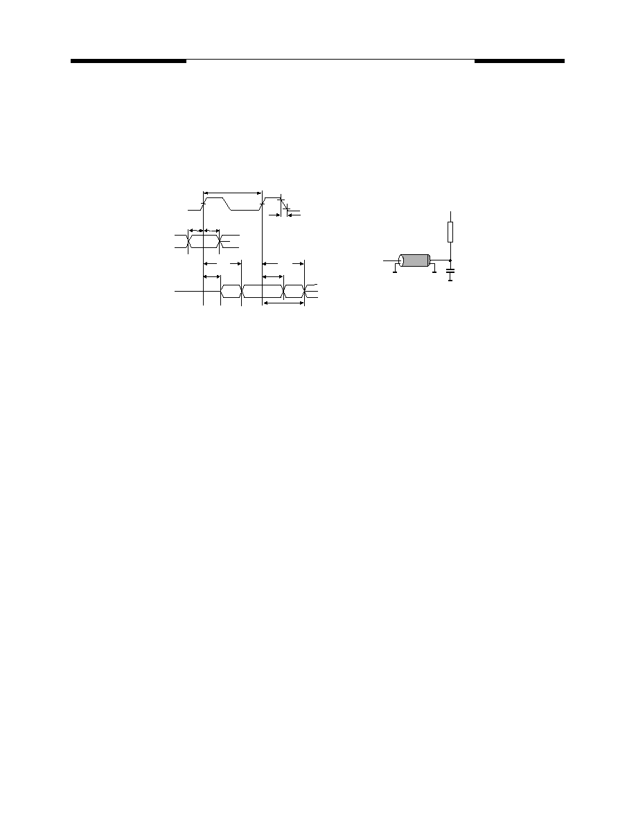
Referenced to the time which the output achieves the open circuit condition, not to output voltage levels
1.4V
1.4V
tCS
tCH
tAC
tAC
tLZ
tOH
tHZ
CLK
COMMAND
OUTPUT
50 pF
I/O
Z=50 Ohm
+ 1.4 V
50 Ohm
VIH
VIL
t
T
Figure 1.
tCK

15
V54C365404VC Rev. 0.6 September 1999
MOSEL VITELIC
V54C365404VC
Timing Diagrams
1. Bank Activate Command Cycle
2. Burst Read Operation
3. Read Interrupted by a Read
4. Read to Write Interval
4.1 Read to Write Interval
4.2 Minimum Read to Write Interval
4.3 Non-Minimum Read to Write Interval
5. Burst Write Operation
6. Write and Read Interrupt
6.1 Write Interrupted by a Write
6.2 Write Interrupted by Read
7. Burst Write & Read with Auto-Precharge
7.1 Burst Write with Auto-Precharge
7.2 Burst Read with Auto-Precharge
8. Burst Termination
8.1 Termination of a Full Page Burst Write Operation
8.2 Termination of a Full Page Burst Write Operation
9. AC- Parameters
9.1 AC Parameters for a Write Timing
9.2 AC Parameters for a Read Timing
10. Mode Register Set
11. Power on Sequence and Auto Refresh (CBR)
12. Clock Suspension (using CKE)
12.1 Clock Suspension During Burst Read CAS Latency = 2
12. 2 Clock Suspension During Burst Read CAS Latency = 3
12. 3 Clock Suspension During Burst Write CAS Latency = 2
12. 4 Clock Suspension During Burst Write CAS Latency = 3
13. Power Down Mode and Clock Suspend
14. Self Refresh (Entry and Exit)
15. Auto Refresh (CBR)

16
V54C365404VC Rev. 0.6 September 1999
MOSEL VITELIC
V54C365404VC
Timing Diagrams
(Cont'd)
16. Random Column Read ( Page within same Bank)
16.1 CAS Latency = 2
16.2 CAS Latency = 3
17. Random Column Write ( Page within same Bank)
17.1 CAS Latency = 2
17.2 CAS Latency = 3
18. Random Row Read ( Interleaving Banks) with Precharge
18.1 CAS Latency = 2
18.2 CAS Latency = 3
19. Random Row Write ( Interleaving Banks) with Precharge
19.1 CAS Latency = 2
19.2 CAS Latency = 3
20. Full Page Read Cycle
20.1 CAS Latency = 2
20.2 CAS Latency = 3
21. Full Page Write Cycle
21.1 CAS Latency = 2
21.2 CAS Latency = 3
22. Precharge Termination of a Burst
22.1 CAS Latency = 2
22.2 CAS Latency = 3

17
V54C365404VC Rev. 0.6 September 1999
MOSEL VITELIC
V54C365404VC
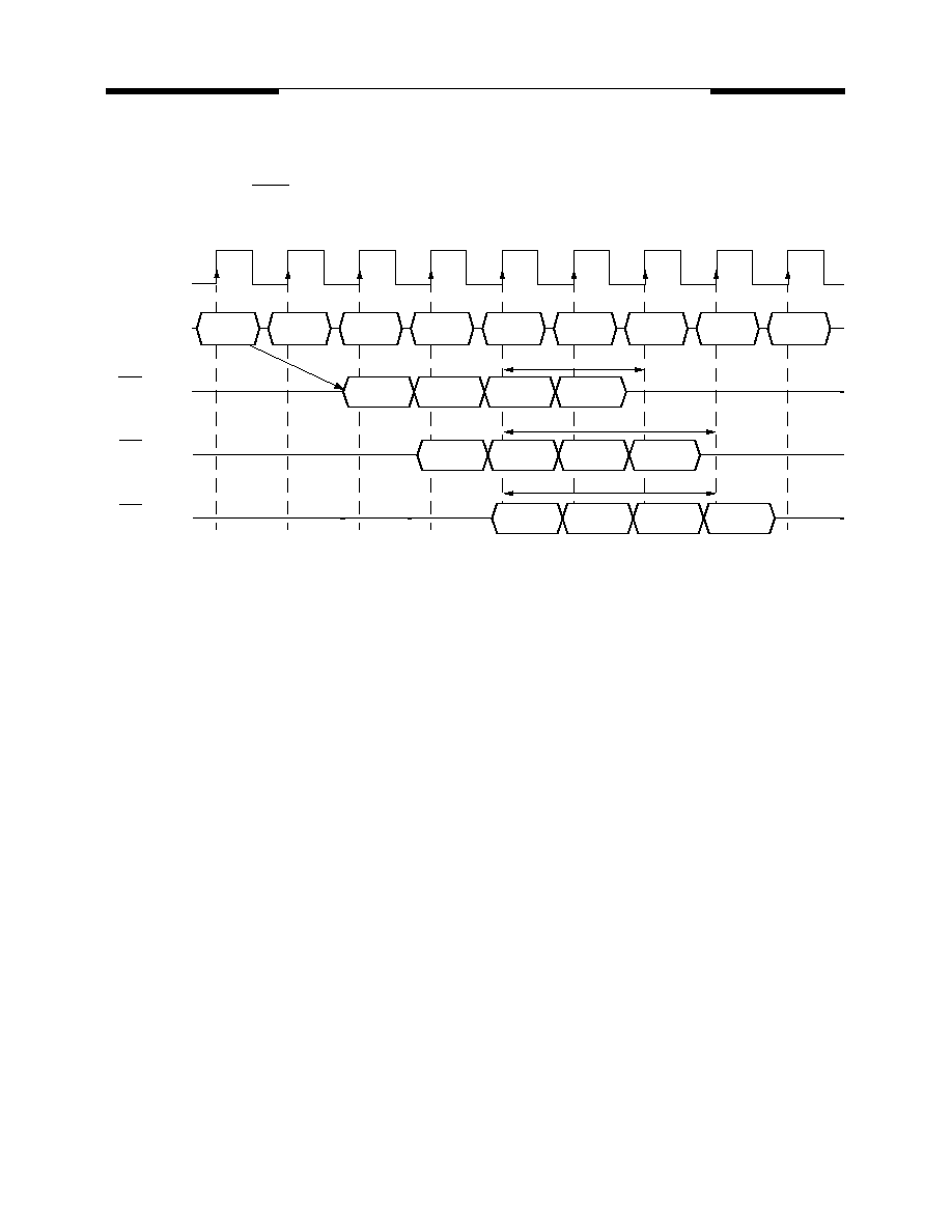
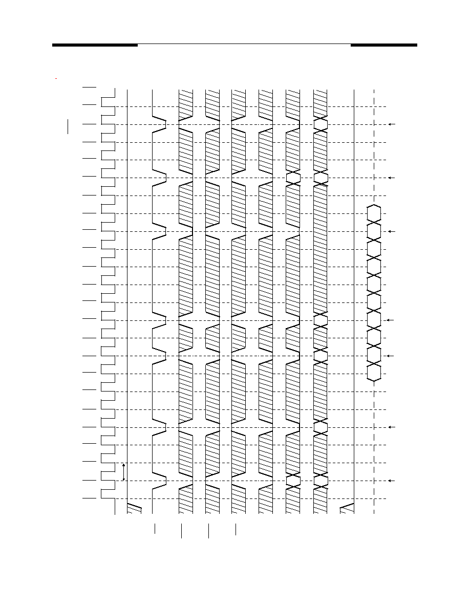
1. Bank Activate Command Cycle
(CAS latency = 3)
2. Burst Read Operation
(Burst Length = 4, CAS latency = 2, 3, 4)
ADDRESS
CLK
T0
T
T1
T
T
T
T
COMMAND
NOP
NOP
NOP
Bank A
Row Addr.
Bank A
Activate
Write A
with Auto
Bank A
Col. Addr.
. . . . . . . . . .
. . . . . . . . . .
. . . . . . . . . .
Bank B
Activate
Bank A
Row Addr.
Bank A
Activate
t
RCD
: "H" or "L"
t
RC
Precharge
t
RRD
Bank B
Row Addr.
COMMAND
READ A
NOP
NOP
NOP
NOP
NOP
NOP
NOP
DOUT A0
CAS latency = 2
t
CK3,
I/O's
CAS latency = 3
t
CK4,
I/O's
CAS latency = 4
DOUT A1
DOUT A2
DOUT A3
NOP
CLK
T0
T2
T1
T3
T4
T5
T6
T7
T8
t
CK2,
I/O's
DOUT A0
DOUT A1
DOUT A2
DOUT A3
DOUT A0
DOUT A1
DOUT A2
DOUT A3

18
V54C365404VC Rev. 0.6 September 1999
MOSEL VITELIC
V54C365404VC
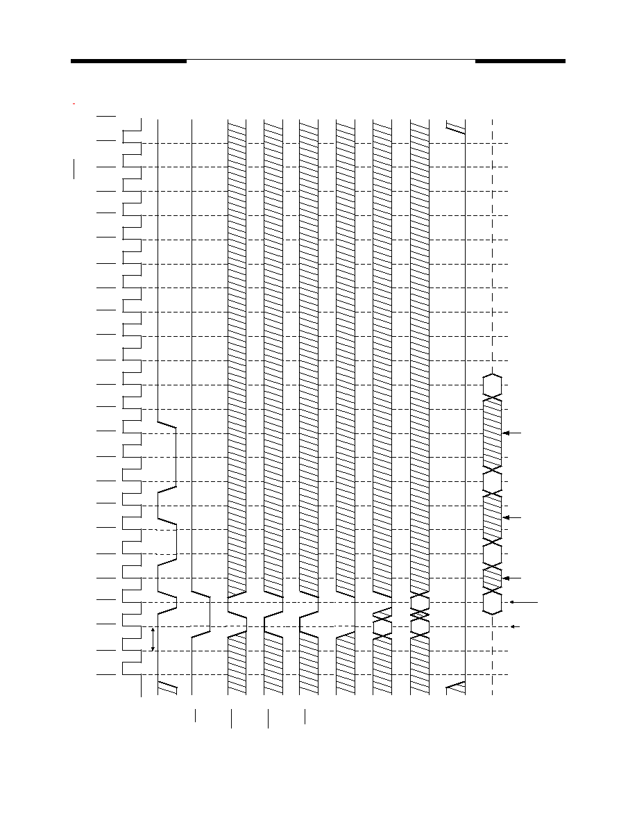
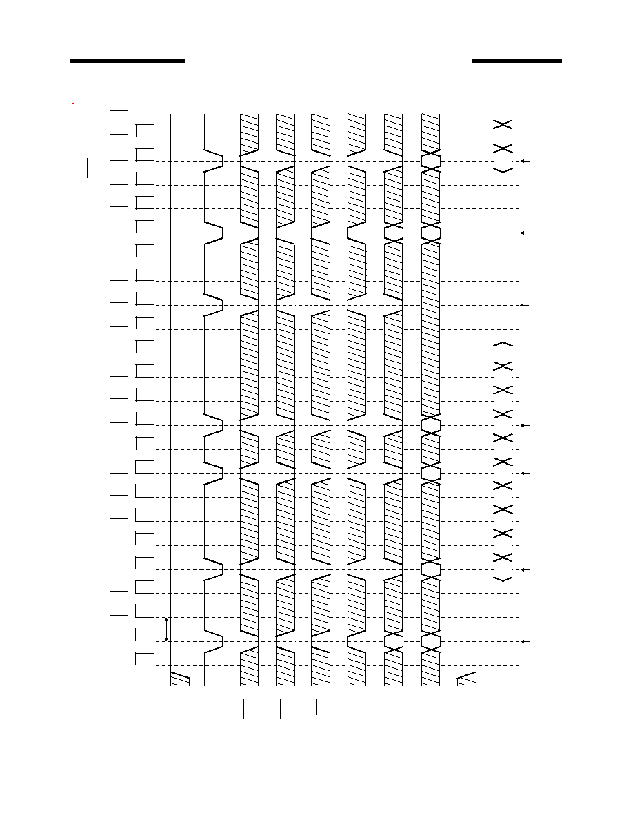
3. Read Interrupted by a Read
(Burst Length = 4, CAS latency = 2, 3, 4)
4.1 Read to Write Interval
(Burst Length = 4, CAS latency = 3)
COMMAND
READ A
READ B
NOP
NOP
NOP
NOP
NOP
NOP
t
CK2,
I/O's
CAS latency = 2
t
CK3,
I/O's
CAS latency = 3
t
CK4,
I/O's
CAS latency = 4
NOP
CLK
T0
T2
T1
T3
T4
T5
T6
T7
T8
DOUT B0
DOUT B1
DOUT B2
DOUT B3
DOUT A0
DOUT B0
DOUT B1
DOUT B2
DOUT B3
DOUT A0
DOUT B0
DOUT B1
DOUT B2
DOUT B3
DOUT A0
COMMAND
NOP
READ A
NOP
NOP
NOP
NOP
WRITE B
NOP
NOP
DQM
DOUT A0
DIN B0
DIN B1
DIN B2
Must be Hi-Z before
the Write Command
I/O's
Minimum delay between the Read and Write Commands = 4+1 = 5 cycles
CLK
T0
T2
T1
T3
T4
T5
T6
T7
T8
t
DQZ
t
DQW
: "H" or "L"

19
V54C365404VC Rev. 0.6 September 1999
MOSEL VITELIC
V54C365404VC
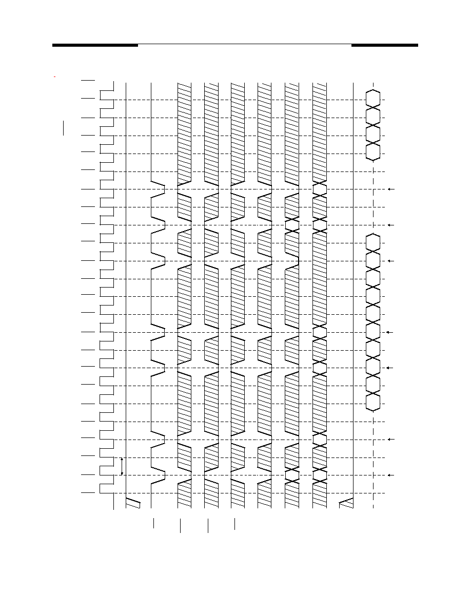
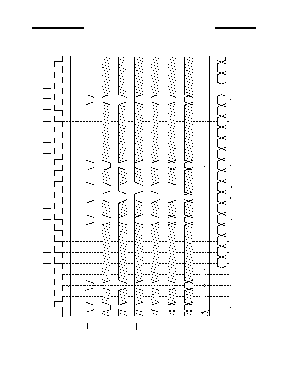
4.2 Minimum Read to Write Interval
(Burst Length = 4, CAS latency = 2)
4.3 Non-Minimum Read to Write Interval
(Burst Length = 4, CAS latency = 2, 3, 4
COMMAND
NOP
BANK A
NOP
READ A
WRITE A
NOP
NOP
NOP
DQM
DIN A0
DIN A1
DIN A2
DIN A3
Must be Hi-Z before
the Write Command
t
CK2,
I/O's
CAS latency = 2
CLK
T0
T2
T1
T3
T4
T5
T6
T7
T8
NOP
ACTIVATE
1 Clk Interval
t
DQZ
t
DQW
: "H" or "L"
NOP
READ A
NOP
NOP
READ A
NOP
WRITE B
NOP
NOP
DQM
DIN B0
DIN B1
DIN B2
t
CK1,
I/O's
CAS latency = 2
t
CK2,
I/O's
CAS latency = 3
CLK
T0
T2
T1
T3
T4
T5
T6
T7
T8
DOUT A0
DIN B0
DIN B1
DIN B2
COMMAND
DIN B0
DIN B1
DIN B2
DOUT A1
DOUT A0
Must be Hi-Z before
the Write Command
t
CK3,
I/O's
CAS latency = 4
t
DQZ
t
DQW
: "H" or "L"

20
V54C365404VC Rev. 0.6 September 1999
MOSEL VITELIC
V54C365404VC
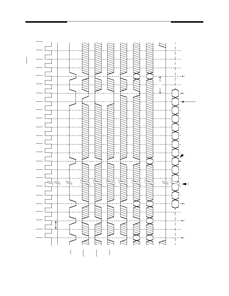
5. Burst Write Operation
(Burst Length = 4, CAS latency = 2, 3, or 4)
6.1 Write Interrupted by a Write
(Burst Length = 4, CAS latency = 2, 3, or 4)
COMMAND
NOP
WRITE A
NOP
NOP
NOP
NOP
NOP
NOP
I/O's
DIN A0
DIN A1
DIN A2
DIN A3
NOP
CLK
T0
T2
T1
T3
T4
T5
T6
T7
T8
Extra data is ignored after
The first data element and the Write
are registered on the same clock edge.
termination of a Burst.
don't care
COMMAND
NOP
WRITE A
WRITE B
NOP
NOP
NOP
NOP
NOP
I/O's
DIN A0
DIN B0
DIN B1
DIN B2
NOP
DIN B3
CLK
T0
T2
T1
T3
T4
T5
T6
T7
T8
1 Clk Interval

21
V54C365404VC Rev. 0.6 September 1999
MOSEL VITELIC
V54C365404VC
6.2 Write Interrupted by a Read
(Burst Length = 4, CAS latency = 2, 3, 4)
7. Burst Write with Auto-Precharge
Burst Length = 2, CAS latency = 2, 3, 4)
COMMAND
NOP
WRITE A
READ B
NOP
NOP
NOP
NOP
NOP
NOP
t
CK2,
I/O's
CAS latency = 2
DIN A0
t
CK3,
I/O's
CAS latency = 3
DIN A0
t
CK4,
I/O's
CAS latency = 4
DIN A0
CLK
T0
T2
T1
T3
T4
T5
T6
T7
T8
Input data for the Write is ignored.
DOUT B3
DOUT B0
DOUT B1
DOUT B2
DOUT B3
DOUT B0
DOUT B1
DOUT B2
don't care
don't care
don't care
don't care
don't care
don't care
DOUT B0
DOUT B1
DOUT B2
Input data must be removed from the I/O's at least one clock
cycle before the Read dataAPpears on the outputs to avoid
data contention.
COMMAND
NOP
NOP
NOP
WRITE A
Auto-Precharge
CLK
T0
T2
T1
T3
T4
T5
T6
T7
T8
NOP
BANK A
ACTIVE
NOP
NOP
DIN A0
DIN A1
DIN A0
DIN A1
*
*
I/O's
CAS latency = 3
I/O's
CAS latency = 2
I/O's
CAS latency = 4
Begin Autoprecharge
Bank can be reactivated after trp
*
t
WR
t
WR
t
RP
t
RP
DIN A0
DIN A1
t
WR
t
RP
NOP
*
22
V54C365404VC Rev. 0.6 September 1999
MOSEL VITELIC
V54C365404VC
7.2 Burst Read with Auto-Precharge
Burst Length = 4, CAS latency = 2, 3, 4)
COMMAND
NOP
WRITE A
READ B
NOP
NOP
NOP
NOP
NOP
NOP
t
CK2,
I/O's
CAS latency = 2
t
CK3,
I/O's
CAS latency = 3
t
CK4,
I/O's
CAS latency = 4
CLK
T0
T2
T1
T3
T4
T5
T6
T7
T8
DOUT A3
DOUT A
tRP
tRP
tRP
*
*
*
*
0
DOUT A1
DOUT A2
DOUT A3
DOUT A
Begin Autoprecharge
Bank can be reactivated after tRP
0
DOUT A1
DOUT A2
DOUT A3
DOUT A0
DOUT A1
DOUT A2

23
V54C365404VC Rev. 0.6 September 1999
MOSEL VITELIC
V54C365404VC
8.1 Termination of a Full Page Burst Read Operation
(CAS latency = 2, 3, 4)
8.2 Termination of a Full Page Burst Write Operation
(CAS latency = 2, 3, 4)
COMMAND
READ A
NOP
NOP
NOP
Burst
NOP
NOP
NOP
NOP
t
CK2,
I/O's
CAS latency = 2
t
CK3,
I/O's
CAS latency = 3
t
CK4,
I/O's
CAS latency = 4
Stop
CLK
T0
T2
T1
T3
T4
T5
T6
T7
T8
The burst ends after a delay equal to the CAS latency.
DOUT A0
DOUT A1
DOUT A2
DOUT A3
DOUT A0
DOUT A1
DOUT A2
DOUT A3
DOUT A0
DOUT A1
DOUT A2
DOUT A3
COMMAND
NOP
WRITE A
NOP
NOP
Burst
NOP
NOP
NOP
NOP
DIN A0
DIN A1
DIN A2
Stop
CLK
T0
T2
T1
T3
T4
T5
T6
T7
T8
Input data for the Write is masked.
I/O's
CAS latency = 2,3,4
don't care

24
V54C365404VC Rev. 0.6 September 1999
MOSEL VITELIC
V54C365404VC
CLK
CKE
CS
I/O
RAS
CAS
WE
BA
DQM
9.1 A
C
P
arameter
s f
or
Write
Timing
T2
T3
T4
T0
T1
T6
T7
T8
T9
T5
T11
T12
T13
T14
T10
T16
T17
T18
T19
T15
T22
T20
T21
Hi-Z
AP
Burst Length = 4,
CAS
Latency = 2
Addr
t
CKS
t
CS
t
CH
t
CKH
t
AS
t
RCD
t
RC
t
RP
t
DS
Activate
Command
Bank A
Write with
Auto Precharge
Command
Bank A
Activate
Command
Bank B
Write with
Auto Precharge
Command
Bank B
Activate
Command
Bank A
Write
Command
Bank A
Precharge
Command
Bank A
Activate
Command
Bank A
t
DH
Ax0
Ax3
Ax2
Ax1
Bx0
Bx3
Bx2
Bx1
Ay0
Ay3
Ay2
Ay1
t
CK2
t
CH
t
CL
Begin Auto Precharge
Bank A
Begin Auto Precharge
Bank B
t
WR
t
RRD
Activate
Command
Bank B
RAy
CBx
RAy
RAy
RBx
RBx
CAx
RBy
RBy
RAz
RAz
RAx
RAx
t
AH

25
V54C365404VC Rev. 0.6 September 1999
MOSEL VITELIC
V54C365404VC
\
CLK
CKE
CS
I/O
RAS
CAS
WE
BA
DQM
9.2
AC Parameters for Read T
iming
T2
T3
T4
T0
T1
T6
T7
T8
T9
T5
T11
T12
T13
T10
Hi-Z
AP
Burst Length = 2,
CAS
Latency = 2
Addr
t
CS
t
CH
t
CKH
t
AS
t
AH
t
RRD
t
RCD
t
RAS
t
LZ
Activate
Command
Bank A
Activate
Command
Bank B
Activate
Command
Bank A
Precharge
Command
Bank A
t
CKS
t
CK2
Ax0
Ax1
Read
Command
Bank A
Read with
Auto Precharge
Command
Bank
B
t
RC
t
RP
t
AC2
t
AC2
t
OH
t
HZ
t
CH
t
CL
Bx0
Begin Auto
Precharge
Bank B
Bx1
t
HZ
RBx
RAy
RBx
RBx
RAy
CAx
RAx
RAx

26
V54C365404VC Rev. 0.6 September 1999
MOSEL VITELIC
V54C365404VC
\
10.
Mode Register Set
CLK
CKE
CS
RAS
CAS
WE
BA
T2
T3
T4
T0
T1
T6
T7
T8
T9
T5
T11
T12
T13
T14
T10
T16
T17
T18
T19
T15
T22
T20
T21
AP
Addr
Precharge
Command
All Banks
Mode Register
Set Command
Any
Command
Address Key
2 Clock min.

27
V54C365404VC Rev. 0.6 September 1999
MOSEL VITELIC
V54C365404VC
\
11.
P
o
wer on Sequence and A
uto Refresh (CBR)
CLK
CKE
CS
I/O
RAS
CAS
WE
BA
DQM
TT
T
T0
TT
T
TT
T
T
T
TT
T1
T
T
TT
TT
T
T
Hi-Z
AP
Addr
Precharge
Command
All Banks
t
RP
Minimum of 2 Refresh Cycles are required
1st Auto Refresh
Command
t
RC
High level
is required
2nd Auto Refresh
Command
Inputs must be
stable for 200
�
s
Any
Command
2 Clock min.
Mode Register
Address Key
Set Command

28
V54C365404VC Rev. 0.6 September 1999
MOSEL VITELIC
V54C365404VC
\
)
12.1 Cloc
k Suspension During Burst Read (Using CKE) (1 of 3)
Burst Length = 4,
CAS
Latency = 1
CLK
CKE
CS
I/O
RAS
CAS
WE
BA
DQM
T2
T3
T4
T0
T1
T6
T7
T8
T9
T5
T11
T12
T13
T14
T10
T16
T17
T18
T19
T15
T22
T20
T21
Hi-Z
AP
Addr
CAx
RAx
Ax0
Ax1
Ax2
Ax3
Activate
Command
Bank A
Read
Command
Bank A
Clock Suspend
2 Cycles
Clock Suspend
1 Cycle
Clock Suspend
3 Cycles
RAx
t
HZ
t
CK1

29
V54C365404VC Rev. 0.6 September 1999
MOSEL VITELIC
V54C365404VC
\
)
12.2 Cloc
k Suspension During Burst Read (Using CKE) (2 of 3)
Burst Length = 4,
CAS
Latency = 2
CLK
CKE
CS
I/O
RAS
CAS
WE
BA
DQM
T2
T3
T4
T0
T1
T6
T7
T8
T9
T5
T11
T12
T13
T14
T10
T16
T17
T18
T19
T15
T22
T20
T21
Hi-Z
AP
Addr
CAx
RAx
Ax0
Ax1
Ax2
Ax3
Activate
Command
Bank A
Clock Suspend
2 Cycles
Clock Suspend
1 Cycle
Clock Suspend
3 Cycles
RAx
Read
Command
Bank A
t
HZ
t
CK2

30
V54C365404VC Rev. 0.6 September 1999
MOSEL VITELIC
V54C365404VC
)
12.3 Cloc
k Suspension During Burst Read (Using CKE) (3 of 3)
Burst Length = 4,
CAS
Latency = 3
CLK
CKE
CS
I/O
RAS
CAS
WE
BA
DQM
T2
T3
T4
T0
T1
T6
T7
T8
T9
T5
T11
T12
T13
T14
T10
T16
T17
T18
T19
T15
T22
T20
T21
Hi-Z
AP
Addr
RAx
Ax0
Ax1
Ax2
Ax3
Activate
Command
Bank A
Clock Suspend
2 Cycles
Clock Suspend
1 Cycle
Clock Suspend
3 Cycles
RAx
Read
Command
Bank A
CAx
t
HZ
t
CK3
31
V54C365404VC Rev. 0.6 September 1999
MOSEL VITELIC
V54C365404VC
\
)
12.4 Cloc
k Suspension During Burst
Write (Using CKE) (1 of 3)
Burst Length = 4,
CAS
Latency = 1
CLK
CKE
CS
I/O
RAS
CAS
WE
BA
DQM
T2
T3
T4
T0
T1
T6
T7
T8
T9
T5
T11
T12
T13
T14
T10
T16
T17
T18
T19
T15
T22
T20
T21
Hi-Z
AP
Addr
CAx
RAx
Activate
Command
Bank A
Write
Command
Bank A
Clock Suspend
1 Cycle
Clock Suspend
2 Cycles
Clock Suspend
3 Cycles
DAx3
DAx2
DAx0
DAx1
RAx
t
CK1

32
V54C365404VC Rev. 0.6 September 1999
MOSEL VITELIC
V54C365404VC
\
13.
P
o
wer Do
wn Mode and Cloc
k Suspend
Burst Length = 4,
CAS
Latency = 2
CLK
CKE
CS
I/O
RAS
CAS
WE
BA
DQM
T2
T3
T4
T0
T1
T6
T7
T8
T9
T5
T11
T12
T13
T14
T10
T16
T17
T18
T19
T15
T22
T20
T21
Hi-Z
AP
Addr
t
CKSP
t
CKSP
CAx
RAx
RAx
Ax2
Ax0
Ax1
Ax3
Activate
Command
Bank A
Clock Suspend
Mode Entry
Clock Suspend
Mode Exit
Read
Command
Bank A
Clock Mask
Start
Clock Mask
End
Precharge
Command
Bank A
Power Down
Mode Entry
Power Down
Mode Exit
t
HZ
Any
Command
t
CK2

33
V54C365404VC Rev. 0.6 September 1999
MOSEL VITELIC
V54C365404VC
14.
Self Refresh (Entr
y and Exit)
BA
Addr
AP
t
CLK
CKE
CS
I/O
RAS
CAS
WE
DQM
T2
T3
T4
T0
T1
T
T
TT
T5
T
T
TT
T
T
T
TT
TT
T
T
Hi-Z
All Banks
must be idle
Self Refresh
Entry
Begin Self Refresh
Exit Command
t
SREX
Self Refresh Exit
Command issued
Self Refresh
Exit
t
RC
CKS

34
V54C365404VC Rev. 0.6 September 1999
MOSEL VITELIC
V54C365404VC
\
15.
A
uto Refresh (CBR)
Burst Length = 4,
CAS
Latency = 2
CLK
CKE
CS
I/O
RAS
CAS
WE
BA
DQM
T2
T3
T4
T0
T1
T6
T7
T8
T9
T5
T11
T12
T13
T14
T10
T16
T17
T18
T19
T15
T22
T20
T21
Hi-Z
AP
Addr
Ax0
Ax1
Activate
Command
Read
Command
Precharge
Command
Auto Refresh
Command
Auto Refresh
Command
t
RC
t
RP
t
RC
t
CK2
All Banks
CAx
RAx
RAx
Bank A
Bank A
Ax2
Ax3
(Minimum Interval)
35
V54C365404VC Rev. 0.6 September 1999
MOSEL VITELIC
V54C365404VC
\
)
16.1 Random Column Read (P
a
g
e within same Bank) (1 of 2)
Burst Length = 4,
CAS
Latency = 2
CLK
CKE
CS
I/O
RAS
CAS
WE
BA
DQM
T2
T3
T4
T0
T1
T6
T7
T8
T9
T5
T11
T12
T13
T14
T10
T16
T17
T18
T19
T15
T22
T20
T21
Hi-Z
AP
Addr
Activate
Command
Bank A
CAx
Read
Command
Bank A
CAy
Read
Command
Bank A
Aw0
Aw1
Aw2
Aw3
Ax0
Ax1
Ay0
Ay1
Az0
Az1
Az2
Az3
Ay2
Ay3
CAw
Read
Command
Bank A
RAw
RAw
Precharge
Command
Bank A
Activate
Command
Bank A
CAz
Read
Command
Bank A
RAz
RAz
t
CK2
36
V54C365404VC Rev. 0.6 September 1999
MOSEL VITELIC
V54C365404VC
\
)
16.2 Random Column Read (P
a
g
e within same Bank) (2 of 2)
Burst Length = 4,
CAS
Latency = 3
CLK
CKE
CS
I/O
RAS
CAS
WE
BA
DQM
T2
T3
T4
T0
T1
T6
T7
T8
T9
T5
T11
T12
T13
T14
T10
T16
T17
T18
T19
T15
T22
T20
T21
Hi-Z
AP
Addr
Activate
Command
Bank A
CAx
Read
Command
Bank A
CAy
Read
Command
Bank A
Aw0
Aw1
Aw2
Aw3
Ax0
Ax1
Ay0
Ay1
Ay2
Ay3
CAw
Read
Command
Bank A
RAw
RAw
Precharge
Command
Bank A
Activate
Command
Bank A
CAz
Read
Command
Bank A
RAz
RAz
t
CK3

37
V54C365404VC Rev. 0.6 September 1999
MOSEL VITELIC
V54C365404VC
\
)
17.1 Random Column
Write (P
a
g
e within same Bank) (1 of 2)
Burst Length = 4,
CAS
Latency = 2
CLK
CKE
CS
I/O
RAS
CAS
WE
BA
DQM
T2
T3
T4
T0
T1
T6
T7
T8
T9
T5
T11
T12
T13
T14
T10
T16
T17
T18
T19
T15
T22
T20
T21
Hi-Z
AP
Addr
CBx
Write
Command
Bank B
CBy
Write
Command
Bank B
Precharge
Command
Bank B
DBw0
DBw3
DBw2
DBw1
DBx1
DBx0
DBy0
DBy3
DBy2
DBy1
DBz0
DBz3
DBz2
DBz1
t
CK2
Activate
Command
Bank B
CAx
Write
Command
Bank B
RAw
RAw
Activate
Command
Bank B
CBz
Write
Command
Bank B
RBz
RBz
Activate
Command
Bank B
CBz
Write
Command
Bank B
RBz
RBz
38
V54C365404VC Rev. 0.6 September 1999
MOSEL VITELIC
V54C365404VC
\
)
17.2 Random Column
Write (P
a
g
e within same Bank) (2 of 2)
Burst Length = 4,
CAS
Latency = 3
CLK
CKE
CS
I/O
RAS
CAS
WE
BA
DQM
T2
T3
T4
T0
T1
T6
T7
T8
T9
T5
T11
T12
T13
T14
T10
T16
T17
T18
T19
T15
T22
T20
T21
Hi-Z
AP
Addr
CBx
Write
Command
Bank B
CBy
Write
Command
Bank B
Precharge
Command
Bank B
DBw0
DBw3
DBw2
DBw1
DBx1
DBx0
DBy0
DBy3
DBy2
DBy1
DBz0
DBz1
t
CK3
Activate
Command
Bank B
CBz
Write
Command
Bank B
RBz
RBz
Activate
Command
Bank B
CBz
Write
Command
Bank B
RBz
RBz
39
V54C365404VC Rev. 0.6 September 1999
MOSEL VITELIC
V54C365404VC
18.1 Random Row Read (Interlea
ving Banks) (1 of 2)
Burst Length = 8,
CAS
Latency = 2
CLK
CKE
CS
I/O
RAS
CAS
WE
A11(BS)
DQM
T2
T3
T4
T0
T1
T6
T7
T8
T9
T5
T11
T12
T13
T14
T10
T16
T17
T18
T19
T15
T22
T20
T21
Hi-Z
A10
A0 - A9
CBy
Read
Command
Bank B
Read
Command
Bank A
Bx0
Bx1
Bx2
Bx3
Bx4
Bx5
Bx6
Bx7
By0
By1
t
CK2
High
t
RCD
t
AC2
t
RP
CAx
Precharge
Command
Bank B
Ax0
Ax1
Ax2
Ax3
Ax4
Ax5
Ax6
Ax7
Activate
Command
Bank B
RBx
RBx
Activate
Command
Bank A
RAx
RAx
CBx
Read
Command
Bank B
Activate
Command
Bank B
RBy
RBy

40
V54C365404VC Rev. 0.6 September 1999
MOSEL VITELIC
V54C365404VC
18.
2 Random Ro
w Read (Interlea
ving Banks) (2 of 2)
Burst Length = 8,
CAS
Latency = 3
CLK
CKE
CS
I/O
RAS
CAS
WE
A11(BS)
DQM
T2
T3
T4
T0
T1
T6
T7
T8
T9
T5
T11
T12
T13
T14
T10
T16
T17
T18
T19
T15
T22
T20
T21
Hi-Z
A10
A0 - A9
CBy
Read
Command
Bank B
By0
t
CK3
High
t
AC3
Activate
Command
Bank B
RBx
RBx
Activate
Command
Bank A
RAx
RAx
CBx
Read
Command
Bank B
Activate
Command
Bank B
RBy
RBy
t
RCD
Precharge
Command
Bank B
CAx
Read
Command
Bank A
t
RP
Bx0
Bx1
Bx2
Bx3
Bx4
Bx5
Bx6
Bx7
Ax0
Ax1
Ax2
Ax3
Ax4
Ax5
Ax6
Ax7
Precharge
Command
Bank A

41
V54C365404VC Rev. 0.6 September 1999
MOSEL VITELIC
V54C365404VC
19.1 Random Row
Write (Interlea
ving Banks) (1 of 2)
Burst Length = 8,
CAS
Latency = 2
CLK
CKE
CS
I/O
RAS
CAS
WE
A11(BS)
DQM
T2
T3
T4
T0
T1
T6
T7
T8
T9
T5
T11
T12
T13
T14
T10
T16
T17
T18
T19
T15
T22
T20
T21
Hi-Z
A10
A0 - A9
t
CK2
High
t
RCD
t
RP
Write
Command
Bank A
CAy
DAx0
DAx3
DAx2
DAx1
DAx4
DAx7
DAx6
DAx5
DBx0
DBx3
DBx2
DBx1
DBx4
DBx7
DBx6
DBx5
DAy0
DAy3
DAy2
DAy1
t
DPL
Write
Command
Bank A
CAX
Activate
Command
Bank A
RAx
RAx
Activate
Command
Bank B
RBx
RBx
CBx
Precharge
Command
Bank A
Write
Command
Bank B
Activate
Command
Bank A
RAy
RAy
CAy
Precharge
Command
Bank B
Write
Command
Bank A
DAy4
t
DPL

42
V54C365404VC Rev. 0.6 September 1999
MOSEL VITELIC
V54C365404VC
19.2 Random Row
Write (Interlea
ving Banks) (2 of 2)
Burst Length = 8,
CAS
Latency = 3
CLK
CKE
CS
I/O
RAS
CAS
WE
A11(BS)
DQM
T2
T3
T4
T0
T1
T6
T7
T8
T9
T5
T11
T12
T13
T14
T10
T16
T17
T18
T19
T15
T22
T20
T21
Hi-Z
A10
A0 - A9
t
CK3
High
DAx0
DAx3
DAx2
DAx1
DAx4
DAx7
DAx6
DAx5
DBx0
DBx3
DBx2
DBx1
DBx4
DBx7
DBx6
DBx5
DAy2
DAy1
DAy0
Write
Command
Bank A
CAX
Activate
Command
Bank B
RBx
RBx
Activate
Command
Bank A
RAy
RAy
DAy3
t
DPL
CBx
Write
Command
Bank B
Precharge
Command
Bank A
Write
Command
Bank A
CAy
Precharge
Command
Bank B
t
RP
t
DPL
t
RCD
Activate
Command
Bank A
RAx
RAx
43
V54C365404VC Rev. 0.6 September 1999
MOSEL VITELIC
V54C365404VC
\
20.1 Full P
a
g
e
Read Cyc
le (1 of 2)
Burst Length = Full Page,
CAS
Latency = 2
CLK
CKE
CS
I/O
RAS
CAS
WE
BA
DQM
T2
T3
T4
T0
T1
T6
T
TT
T5
T
T
TT
T
T
T
TT
TT
T
T
Hi-Z
AP
Addr
t
CK2
High
Ax
Ax+1
Ax-1
Ax-2
Ax+2
Ax
Bx
Bx+1
Bx+5
Bx+4
Bx+3
Bx+2
Ax+1
Bx+6
CBx
Read
Command
Bank B
Precharge
Command
Bank B
Burst Stop
Command
CAx
Read
Command
Bank A
Activate
Command
Bank A
RAx
RAx
Activate
Command
Bank B
RBx
RBx
Activate
Command
Bank B
RBy
RBy
t
RP
Full Page burst operation does not
terminate when the burst length is satisfied;
the burst counter increments and continues
The burst counter wraps
from the highest order
page address back to zero
during this time interval.
bursting beginning with the starting address.

44
V54C365404VC Rev. 0.6 September 1999
MOSEL VITELIC
V54C365404VC
\
20.2 Full P
a
g
e
Read Cyc
le (2 of 2)
Burst Length = Full Page,
CAS
Latency = 3
CLK
CKE
CS
I/O
RAS
CAS
WE
BA
DQM
T2
T3
T4
T0
T1
T6
T7
T8
T
T5
T
T
TT
T
T
T
TT
TT
T
T
Hi-Z
AP
Addr
t
CK3
High
Ax
Ax+1
Ax-1
Ax-2
Ax+2
Ax
Bx
Bx+1
Bx+5
Bx+4
Bx+3
Bx+2
Ax+1
CBx
Read
Command
Bank B
Precharge
Command
Bank B
Burst Stop
Command
CAx
Read
Command
Bank A
Activate
Command
Bank A
RAx
RAx
Activate
Command
Bank B
RBx
RBx
Activate
Command
Bank B
RBy
RBy
t
RRD
Full Page burst operation does not
The burst counter wraps
from the highest order
page address back to zero
during this time interval.
terminate when the length is
satisfied; the burst counter
increments and continues
bursting beginning with
the starting address.

45
V54C365404VC Rev. 0.6 September 1999
MOSEL VITELIC
V54C365404VC
\
)
21.1 Full P
a
g
e
Write Cyc
le (1 of 2)
Burst Length = Full Page,
CAS
Latency = 2
CLK
CKE
CS
I/O
RAS
CAS
WE
BA
DQM
T2
T3
T4
T0
T1
T
T
TT
T5
T
T
TT
T
T
T
TT
TT
T
T
Hi-Z
AP
Addr
t
CK2
High
CBx
Write
Command
Bank B
Precharge
Command
Bank B
Burst Stop
Command
CAx
Write
Command
Bank A
Activate
Command
Bank A
RAx
RAx
Activate
Command
Bank B
RBx
RBx
Activate
Command
Bank B
RBy
RBy
Data is ignored.
DAx
DAx+1
DAx-1
DAx+3
DAx+2
DAx
DBx
DBx+1
DAx+1
DBx+3
DBx+2
DBx+4
DBx+5
DBx+6
Full Page burst operation does not
terminate when the burst length is satisfied;
the burst counter increments and continues
The burst counter wraps
from the highest order
page address back to zero
during this time interval.
bursting beginning with the starting address.

46
V54C365404VC Rev. 0.6 September 1999
MOSEL VITELIC
V54C365404VC
21.2 Full P
a
g
e
Write Cyc
le (2 of 2)
Burst Length = Full Page,
CAS
Latency = 3
CLK
CKE
CS
I/O
RAS
CAS
WE
BA
DQM
T2
T3
T4
T0
T1
T6
T
TT
T5
T
T
TT
T
T
T
TT
TT
T
T
Hi-Z
AP
Addr
t
CK3
High
CBx
Write
Command
Bank B
Precharge
Command
Bank B
Burst Stop
Command
CAx
Write
Command
Bank A
Activate
Command
Bank A
RAx
RAx
Activate
Command
Bank B
RBx
RBx
Activate
Command
Bank B
RBy
RBy
DAx
DAx+1
DAx-1
DAx+3
DAx+2
DAx
DBx
DBx+1
DAx+1
DBx+3
DBx+2
DBx+4
DBx+5
Full Page burst operation does not
The burst counter wraps
from the highest order
page address back to zero
during this time interval.
terminate when the length is
satisfied; the burst counter
increments and continues
bursting beginning with
the starting address.
Data is ignored.

47
V54C365404VC Rev. 0.6 September 1999
MOSEL VITELIC
V54C365404VC
22.1 Prechar
g
e
T
ermination of a Burst (1 of 2)
Burst Length = 8 or Full Page,
CAS
Latency = 2
CLK
CKE
CS
I/O
RAS
CAS
WE
BA
DQM
T2
T3
T4
T0
T1
T6
T7
T8
T9
T5
T11
T12
T13
T14
T10
T16
T17
T18
T19
T15
T22
T20
T21
Hi-Z
AP
Addr
t
CK2
Precharge
Command
Bank A
DAx0
DAx3
DAx2
DAx1
Precharge Termination
of a Write Burst. Write
data is masked.
Ay0
Ay1
Ay2
Precharge Termination
of a Read Burst.
Precharge
Command
Bank A
t
RP
Activate
Command
Bank A
RAx
RAx
Write
Command
Bank A
CAx
CAy
Read
Command
Bank A
High
Activate
Command
Bank A
RAy
RAy
t
RP
Activate
Command
Bank A
RAz
RAz
CAz
Read
Command
Bank A
Az0
Az1
Az2
Precharge
Command
Bank A
t
RP

48
V54C365404VC Rev. 0.6 September 1999
MOSEL VITELIC
V54C365404VC
22.2 Prechar
g
e
T
ermination of a Burst (2 of 2)
Burst Length = 4,8 or Full Page,
CAS
Latency = 3
CLK
CKE
CS
I/O
RAS
CAS
WE
BA
DQM
T2
T3
T4
T0
T1
T6
T7
T8
T9
T5
T11
T12
T13
T14
T10
T16
T17
T18
T19
T15
T22
T20
T21
Hi-Z
AP
Addr
t
CK3
Precharge
Command
Bank A
DAx0
Precharge Termination
of a Write Burst.
Write Data
is masked
Ay0
Ay1
Ay2
Precharge Termination
Precharge
Command
Bank A
t
RP
Activate
Command
Bank A
RAx
RAx
Write
Command
Bank A
CAx
CAy
Read
Command
Bank A
High
Activate
Command
Bank A
RAy
RAy
t
RP
Activate
Command
Bank A
RAz
RAz
of a Read Burst.

49
V54C365404VC Rev. 0.6 September 1999
MOSEL VITELIC
V54C365404VC
Complete List of Operation Commands
SDRAM Function Truth Table
CURRENT
STATE
1
CS
RAS
CAS
WE
BS
Addr
ACTION
Idle
H
L
L
L
L
L
L
L
X
H
H
H
L
L
L
L
X
H
H
L
H
H
L
L
X
H
L
X
H
L
H
L
X
X
BS
BS
BS
BS
X
Op-
X
X
X
X
RA
AP
X
Code
NOP or Power Down
NOP
ILLEGAL
2
ILLEGAL
2
Row (&Bank) Active; Latch Row Address
NOP
4
Auto-Refresh or Self-Refresh
5
Mode reg. Access
5
Row Active
H
L
L
L
L
L
L
X
H
H
H
L
L
L
X
H
L
L
H
H
L
X
X
H
L
H
L
X
X
X
BS
BS
BS
BS
X
X
X
CA,AP
CA,AP
X
AP
X
NOP
NOP
Begin Read; Latch CA; DetermineAP
Begin Write; Latch CA; DetermineAP
ILLEGAL
2
Precharge
ILLEGAL
Read
H
L
L
L
L
L
L
L
X
H
H
H
H
L
L
L
X
H
H
L
L
H
H
L
X
H
L
H
L
H
L
X
X
X
BS
BS
BS
BS
BS
X
X
X
X
CA,AP
CA,AP
X
AP
X
NOP (Continue Burst to End;>Row Active)
NOP (Continue Burst to End;>Row Active)
Burst Stop Command > Row Active
Term Burst, New Read, DetermineAP
3
Term Burst, Start Write, DetermineAP
3
ILLEGAL
2
Term Burst, Precharge
ILLEGAL
Write
H
L
L
L
L
L
L
L
X
H
H
H
H
L
L
L
X
H
H
L
L
H
H
L
X
H
L
H
L
H
L
X
X
X
BS
BS
BS
BS
BS
X
X
X
X
CA,AP
CA,AP
X
AP
X
NOP (Continue Burst to End;>Row Active)
NOP (Continue Burst to End;>Row Active)
Burst Stop Command > Row Active
Term Burst, Start Read, DetermineAP
3
Term Burst, New Write, DetermineAP
3
ILLEGAL
2
Term Burst, Precharge
3
ILLEGAL
Read
with
Auto
Precharge
H
L
L
L
L
L
L
L
X
H
H
H
H
L
L
L
X
H
H
L
L
H
H
L
X
H
L
H
L
H
L
X
X
X
BS
BS
X
BS
BS
X
X
X
X
X
X
X
AP
X
NOP (Continue Burst to End;> Precharge)
NOP (Continue Burst to End;> Precharge)
ILLEGAL
2
ILLEGAL
2
ILLEGAL
ILLEGAL
2
ILLEGAL
2
ILLEGAL

50
V54C365404VC Rev. 0.6 September 1999
MOSEL VITELIC
V54C365404VC
SDRAM FUNCTION TRUTH TABLE(continued)
CURRENT
STATE
1
CS
RAS
CAS
WE
BS
Addr
ACTION
Write
with
Auto
Precharge
H
L
L
L
L
L
L
L
X
H
H
H
H
L
L
L
X
H
H
L
L
H
H
L
X
H
L
H
L
H
L
X
X
X
BS
BS
X
BS
BS
X
X
X
X
X
X
X
AP
X
NOP (Continue Burst to End;> Precharge)
NOP (Continue Burst to End;> Precharge)
ILLEGAL
2
ILLEGAL
2
ILLEGAL
ILLEGAL
2
ILLEGAL
2
ILLEGAL
Precharging
H
L
L
L
L
L
L
X
H
H
H
L
L
L
X
H
H
L
H
H
L
X
H
L
X
H
L
X
X
X
BS
BS
BS
BS
X
X
X
X
X
X
AP
X
NOP;> Idle after tRP
NOP;> Idle after tRP
ILLEGAL
2
ILLEGAL
2
ILLEGAL
2
NOP
4
ILLEGAL
Row
Activating
H
L
L
L
L
L
L
X
H
H
H
L
L
L
X
H
H
L
H
H
L
X
H
L
X
H
L
X
X
X
BS
BS
BS
BS
X
X
X
X
X
X
AP
X
NOP;> Row Active after tRCD
NOP;> Row Active after tRCD
ILLEGAL
2
ILLEGAL
2
ILLEGAL
2
ILLEGAL
2
ILLEGAL
Write
Recovering
H
L
L
L
L
L
L
X
H
H
H
L
L
L
X
H
H
L
H
H
L
X
H
L
X
H
L
X
X
X
BS
BS
BS
BS
X
X
X
X
X
X
AP
X
NOP
NOP
ILLEGAL
2
ILLEGAL
2
ILLEGAL
2
ILLEGAL
2
ILLEGAL
Refreshing
H
L
L
L
L
X
H
H
L
L
X
H
L
H
L
X
X
X
X
X
X
X
X
X
X
X
X
X
X
X
NOP;> Idle after tRC
NOP;> Idle after tRC
ILLEGAL
ILLEGAL
ILLEGAL
Mode
Register
Accessing
H
L
L
L
L
X
H
H
H
L
X
H
H
L
X
X
H
L
X
X
X
X
X
X
X
X
X
X
X
X
NOP
NOP
ILLEGAL
ILLEGAL
ILLEGAL

51
V54C365404VC Rev. 0.6 September 1999
MOSEL VITELIC
V54C365404VC
Clock Enable (CKE) Truth Table:
Abbreviations:
RA = Row Address BS = Bank Address
CA = Column Address AP = Auto Precharge
Notes for SDRAM function truth table:
1. Current State is state of the bank determined by BS. All entries assume that CKE was active (HIGH) during the preceding clock cycle.
2. Illegal to bank in specified state; Function may be legal in the bank indicated by BS, depending on the state of that bank.
3. Must satisfy bus contention, bus turn around, and/or write recovery requirements.
4. NOP to bank precharging or in Idle state. May precharge bank(s) indicated by BS (andAP).
5. Illegal if any bank is not Idle.
6. CKE Low to High transition will re-enable CLK and other inputs asynchronously. A minimum setup time must be satisfied before any
command other than EXIT.
7. Power-Down and Self-Refresh can be entered only from the All Banks Idle State.
8. Must be legal command as defined in the SDRAM function truth table.
STATE(n)
CKE
n-1
CKE
n
CS
RAS
CAS
WE
Addr
ACTION
Self-Refresh
6
H
L
L
L
L
L
L
X
H
H
H
H
H
L
X
H
L
L
L
L
X
X
X
H
H
H
L
X
X
X
H
H
L
X
X
X
X
H
L
X
X
X
X
X
X
X
X
X
X
INVALID
EXIT Self-Refresh, Idle after tRC
EXIT Self-Refresh, Idle after tRC
ILLEGAL
ILLEGAL
ILLEGAL
NOP (Maintain Self-Refresh)
Power-Down
H
L
L
L
L
L
L
X
H
H
H
H
H
L
X
H
L
L
L
L
X
X
X
H
H
H
L
X
X
X
H
H
L
X
X
X
X
H
L
X
X
X
X
X
X
X
X
X
X
INVALID
EXIT Power-Down, > Idle.
EXIT Power-Down, > Idle.
ILLEGAL
ILLEGAL
ILLEGAL
NOP (Maintain Low-Power Mode)
All. Banks
Idle
7
H
H
H
H
H
H
H
H
L
H
L
L
L
L
L
L
L
L
X
H
L
L
L
L
L
L
X
X
X
H
H
H
L
L
L
X
X
X
H
H
L
H
L
L
X
X
X
H
L
X
X
H
L
X
X
X
X
X
X
X
X
X
X
Refer to the function truth table
Enter Power- Down
Enter Power- Down
ILLEGAL
ILLEGAL
ILLEGAL
Enter Self-Refresh
ILLEGAL
NOP
Any State
other than
listed above
H
H
L
L
H
L
H
L
X
X
X
X
X
X
X
X
X
X
X
X
X
X
X
X
X
X
X
X
Refer to the function truth table
Begin Clock Suspend next cycle
8
Exit Clock Suspend next cycle
8
.
Maintain Clock Suspend.

52
V54C365404VC Rev. 0.6 September 1999
MOSEL VITELIC
V54C365404VC
Package Diagram
54-Pin Plastic TSOP-II (400 mil)
0.881 -0.01
[22.38 -0.25]
0.031
[0.80]
.004 [0.1]
54
Index Marking
M
28
1
Does not include plastic or metal protrusion of 0.15 max. per side
1
27
0.047 [1.20] MAX
0.04
�
0.002
[1
�
0.05]
Unit in inches [mm]
0.400
�
0.005
[10.16
�
0.13]
0.463
�
0.008
[11.76
�
0.20]
0.006 [0.15] MAX
+0.004
-0.002
0
�
�5
�
0.024
�
0.008
[0.60
�
.020]
1
0.006
+0.01
-0.05
0.15
.008 [0.2]
54x
+0.002
-0.004
0.016
+0.05
-0.10
0.40

53
V54C365404VC Rev. 0.6 September 1999
MOSEL VITELIC
V54C365404VC
Notes

MOSEL VITELIC
WORLDWIDE OFFICES
V54C365404VC
MOSEL VITELIC
3910 N. First Street, San Jose, CA 95134-1501 Ph: (408) 433-6000 Fax: (408) 433-0952 Tlx: 371-9461
� Copyright 1999, MOSEL VITELIC Inc.
9/99
Printed in U.S.A.
U.S. SALES OFFICES
The information in this document is subject to change without
notice.
MOSEL VITELIC makes no commitment to update or keep cur-
rent the information contained in this document. No part of this
document may be copied or reproduced in any form or by any
means without the prior written consent of MOSEL-VITELIC.
MOSEL VITELIC subjects its products to normal quality control
sampling techniques which are intended to provide an assurance
of high quality products suitable for usual commercial applica-
tions. MOSEL VITELIC does not do testing appropriate to provide
100% product quality assurance and does not assume any liabil-
ity for consequential or incidental arising from any use of its prod-
ucts. If such products are to be used in applications in which
personal injury might occur from failure, purchaser must do its
own quality assurance testing appropriate to such applications.
U.S.A.
3910 NORTH FIRST STREET
SAN JOSE, CA 95134
PHONE: 408-433-6000
FAX: 408-433-0952
HONG KONG
19 DAI FU STREET
TAIPO INDUSTRIAL ESTATE
TAIPO, NT, HONG KONG
PHONE: 852-2665-4883
FAX: 852-2664-7535
TAIWAN
7F, NO. 102
MIN-CHUAN E. ROAD, SEC. 3
TAIPEI
PHONE: 886-2-2545-1213
FAX: 886-2-2545-1209
1 CREATION ROAD I
SCIENCE BASED IND. PARK
HSIN CHU, TAIWAN, R.O.C.
PHONE: 886-3-578-3344
FAX: 886-3-579-2838
SINGAPORE
10 ANSON ROAD #23-13
INTERNATIONAL PLAZA
SINGAPORE 079903
PHONE: 65-3231801
FAX: 65-3237013
JAPAN
WBG MARINE WEST 25F
6, NAKASE 2-CHOME
MIHAMA-KU, CHIBA-SHI
CHIBA 261-71
PHONE: 81-43-299-6000
FAX: 81-43-299-6555
IRELAND & UK
BLOCK A UNIT 2
BROOMFIELD BUSINESS PARK
MALAHIDE
CO. DUBLIN, IRELAND
PHONE: +353 1 8038020
FAX: +353 1 8038049
GERMANY
(CONTINENTAL
EUROPE & ISRAEL )
71083 HERRENBERG
BENZSTR. 32
GERMANY
PHONE: +49 7032 2796-0
FAX: +49 7032 2796 22
NORTHWESTERN
3910 NORTH FIRST STREET
SAN JOSE, CA 95134
PHONE: 408-433-6000
FAX: 408-433-0952
NORTHEASTERN
SUITE 436
20 TRAFALGAR SQUARE
NASHUA, NH 03063
PHONE: 603-889-4393
FAX: 603-889-9347
NORTHEASTERN
SUITE 436
20 TRAFALGAR SQUARE
NASHUA, NH 03063
PHONE: 603-889-4393
FAX: 603-889-9347
SOUTHWESTERN
SUITE 200
5150 E. PACIFIC COAST HWY.
LONG BEACH, CA 90804
PHONE: 562-498-3314
FAX: 562-597-2174
CENTRAL &
SOUTHEASTERN
604 FIELDWOOD CIRCLE
RICHARDSON, TX 75081
PHONE: 972-690-1402
FAX: 972-690-0341