MOSEL VITELIC
1
V58C3643204SAT
HIGH PERFORMANCE
3.3 VOLT 2M X 32 DDR SDRAM
4 X 512K X 32
V58C3643204SAT Rev. 1.4 August 2001
PRELIMINARY
45
50
55
60
System Frequency (f
CK
)
225MHz
200 MHz
183 MHz
166 MHz
Clock Cycle Time (t
CK3
)
5 ns
5.5 ns
6 ns
Clock Cycle Time (t
CK4
)
4.5 ns
Features
s
4 banks x 512K x 32 organization
s
High speed data transfer rates with system
frequency up to 225 MHz
s
Data Mask for Write Control (DM)
s
Four Banks controlled by BA0 & BA1
s
Programmable CAS Latency: 3, 4
s
Programmable Wrap Sequence: Sequential
or Interleave
s
Programmable Burst Length:
2, 4, 8 full page for Sequential Type
2, 4, 8 full page for Interleave Type
s
Automatic and Controlled Precharge Command
s
Suspend Mode and Power Down Mode
s
Auto Refresh and Self Refresh
s
Refresh Interval: 2048 cycles/16ms
s
Available in 100-pin TQFP
s
SSTL-2 Compatible I/Os
s
Double Data Rate (DDR)
s
Bidirectional Data Strobe (DQs) for input and
output data, active on both edges
s
On-Chip DLL aligns DQ and DQs transitions with
CLK transitions
s
Differential clock inputs CLK and CLK
s
Power Supply 3.3V ± 0.3V
Description
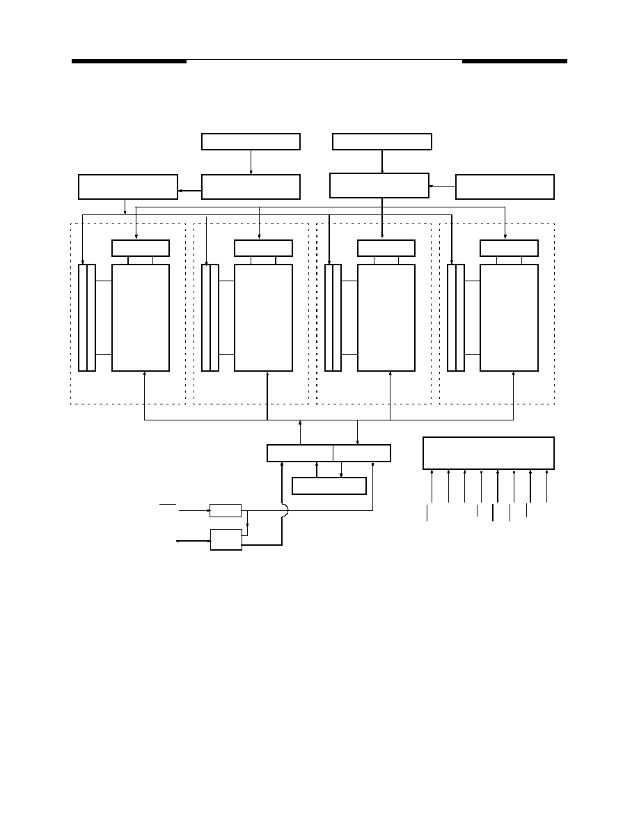
The V58C3643204SAT is a four bank DDR
DRAM organized as 4 banks x 512K x 32. The
V58C3643204SAT
achieves
high
speed
data
transfer rates by employing a chip architecture that
prefetches multiple bits and then synchronizes the
output data to a system clock
All of the control, address, circuits are synchro-
nized with the positive edge of an externally sup-
plied clock. I/O transactions are possible on both
edges of DQS.
Operating the four memory banks in an inter-
leaved fashion allows random access operation to
occur at a higher rate than is possible with standard
DRAMs. A sequential and gapless data rate is pos-
sible depending on burst length, CAS latency and
speed grade of the device.
Device Usage Chart
Operating
Temperature
Range
Package Outline
CLK Cycle Time (ns)
Power
Temperature
Mark
100-pin TQFP
-45
-50
-55
-60
Std.
L
0°C to 70°C
·
·
·
·
·
·
·
Blank
4
V58C3643204SAT Rev. 1.4 August 2001
MOSEL VITELIC
V58C3643204SAT
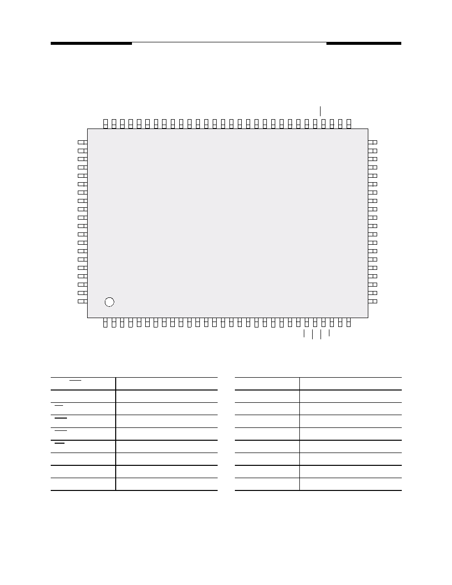
Signal Pin Description
Pin
Type
Signal
Polarity
Function
CLK
CLK
Input
Pulse
Positive
Edge
The system clock input. All inputs except DQs and DMs are sampled on the rising edge
of CLK.
CKE
Input
Level
Active High Activates the CLK signal when high and deactivates the CLK signal when low, thereby
initiates either the Power Down mode, Suspend mode, or the Self Refresh mode.
CS
Input
Pulse
Active Low CS enables the command decoder when low and disables the command decoder when
high. When the command decoder is disabled, new commands are ignored but previous
operations continue.
RAS, CAS
WE
Input
Pulse
Active Low When sampled at the positive rising edge of the clock, CAS, RAS, and WE define the
command to be executed by the SDRAM.
DQS
Input/
Output
Pulse
Active High Active on both edges for data input and output.
Center aligned to input data
Edge aligned to output data
A0 - A10
Input
Level
--
During a Bank Activate command cycle, A0-A10 defines the row address (RA0-RA10)
when sampled at the rising clock edge.
During a Read or Write command cycle, A0-An defines the column address (CA0-CAn)
when sampled at the rising clock edge. CAn depends from the SDRAM organization:
2M x 32 SDRAM CAn = CA7 (Page)
In addition to the column address, A8 is used to invoke autoprecharge operation at the
end of the burst read or write cycle. If A8 is high, autoprecharge is selected and BA0, BA1
defines the bank to be precharged. If A8 is low, autoprecharge is disabled.
During a Precharge command cycle, A8(=AP) is used in conjunction with BA0 and BA1
to control which bank(s) to precharge. If A10 is high, all four banks will be precharged
simultaneously regardless of state of BA0 and BA1.
BA0,
BA1
Input
Level
--
Selects which bank is to be active.
DQx
Input/
Output
Level
--
Data Input/Output pins operate in the same manner as on conventional DRAMs.
DM0-DM3
Input
Pulse
Active High In Write mode, DM has a latency of zero and operates as a word mask by allowing input
data to be written if it is low but blocks the write operation if is high.
VDD, VSS
Supply
Power and ground for the input buffers and the core logic.
VDDQ
VSSQ
Supply
--
--
Isolated power supply and ground for the output buffers to provide improved noise
immunity.
VREF
Input
Level
--
SSTL Reference Voltage for Inputs
5
V58C3643204SAT Rev. 1.4 August 2001
MOSEL VITELIC
V58C3643204SAT
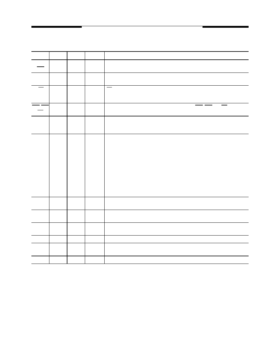
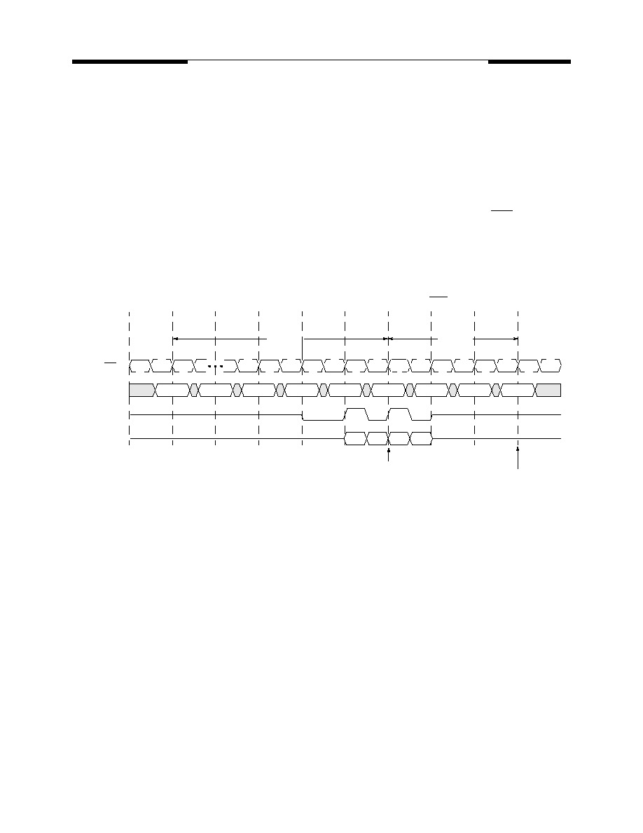
Auto Precharge Operation
The Auto Precharge operation can be issued by having column address A
8
high when a Read or Write com-
mand is issued. If A
10
is low when a Read or Write command is issued, then normal Read or Write burst op-
eration is executed and the bank remains active at the completion of the burst sequence. When the Auto
Precharge command is activated, the active bank automatically begins to precharge at the earliest possible
moment during the Read or Write cycle once t
RAS
(min) is satisfied.
Read with Auto Precharge
If a Read with Auto Precharge command is initiated, the DDR SDRAM will enter the precharge operation
N-clock cycles measured from the last data of the burst read cycle where N is equal to the CAS latency pro-
grammed into the device. Once the autoprecharge operation has begun, the bank cannot be reactivated until
the minimum precharge time (t
RP
) has been satisfied.
Read with Autoprecharge Timing
(CAS Latency = 2; Burst Length = 4)
T0
T1
T2
T3
T4
T5
T6
T7
T8
D
0
D
1
D
2
D
3
Begin Autoprecharge
NOP
BA
R w/AP
NOP
NOP
NOP
NOP
NOP
BA
CK, CK
Command
DQS
DQ
t
RAS
(min)
t
RP
(min)
Earliest Bank A reactivate
T9