
MOSEL VITELIC
1
V58C365164S
64 Mbit DDR SDRAM
4M X 16, 3.3VOLT
V58C365164S Rev. 2.0 January 2003
PRELIMINARY
36
4
5
System Frequency (f
CK
)
275 MHz
250 MHz
200 MHz
Clock Cycle Time (t
CK3
)
3.6 ns
4 ns
5 ns
Clock Cycle Time (t
CK2.5
)
4.3ns
4.8 ns
6 ns
Clock Cycle Time (t
CK2
)
5.4ns
6 ns
7.5 ns
Features
4 banks x 1Mbit x 16 organization
High speed data transfer rates with system
frequency up to 275 MHz
Data Mask for Write Control (DM)
Four Banks controlled by BA0 & BA1
Programmable CAS Latency: 2, 2.5, 3
Programmable Wrap Sequence: Sequential
or Interleave
Programmable Burst Length:
2, 4, 8 for Sequential Type
2, 4, 8 for Interleave Type
Automatic and Controlled Precharge Command
Suspend Mode and Power Down Mode
Auto Refresh and Self Refresh
Refresh Interval: 4096 cycles/64 ms
Available in 66-pin 400 mil TSOP-II
SSTL-2 Compatible I/Os
Double Data Rate (DDR)
Bidirectional Data Strobe (DQs) for input and
output data, active on both edges
On-Chip DLL aligns DQ and DQs transitions with
CLK transitions
Differential clock inputs CLK and CLK
Power supply 3.3V ± 0.3V
VDDQ (I/O) power supply 2.5 + 0.2V
Description
The V58C365164S is a four bank DDR DRAM
organized as 4 banks x 1Mbit x 16. The
V58C365164S achieves high speed data transfer
rates by employing a chip architecture that
prefetches multiple bits and then synchronizes the
output data to a system clock
All of the control, address, circuits are synchro-
nized with the positive edge of an externally sup-
plied clock. I/O transactions are possible on both
edges of DQS.
Operating the four memory banks in an inter-
leaved fashion allows random access operation to
occur at a higher rate than is possible with standard
DRAMs. A sequential and gapless data rate is pos-
sible depending on burst length, CAS latency and
speed grade of the device.
Device Usage Chart
Operating
Temperature
Range
Package Outline
CLK Cycle Time (ns)
Power
Temperature
Mark
JEDEC 66 TSOP II
-36
-4
-5
Std.
L
0∞C to 70∞C
∑
∑
∑
∑
∑
∑
Blank

2
V58C365164S Rev. 2.0 January 2003
MOSEL VITELIC
V58C365164S
66 Pin Plastic TSOP-II
PIN CONFIGURATION
Top View
Pin Names
1
2
3
4
5
6
9
10
11
12
13
14
7
8
15
16
17
18
19
20
21
22
66
65
64
63
62
61
58
57
56
55
54
53
60
59
52
51
50
49
48
47
46
45
23
24
25
44
43
42
26
27
41
40
28
29
30
31
32
33
39
38
37
36
35
34
V
DD
DQ
0
V
DDQ
DQ
1
DQ
2
DQ
3
DQ
4
DQ
5
DQ
6
DQ
7
V
SSQ
V
DDQ
V
SSQ
NC
V
DDQ
LDQS
NC
V
DD
NC
LDM
WE
CAS
RAS
CS
NC
BA0
BA1
V
SS
DQ
15
V
SSQ
DQ
14
DQ
13
V
DDQ
V
SSQ
DQ
10
DQ
9
V
DDQ
DQ
8
NC
DQ
12
DQ
11
V
SSQ
UDQS
NC
V
REF
V
SS
UDM
CLK
CLK
CKE
NC
NC
A11
A9
A10/AP
A0
A1
A2
A3
V
DD
A8
A7
A6
A5
A4
V
SS
64M
DDR SDRAM
CLK, CLK
Differential Clock Input
CKE
Clock Enable
CS
Chip Select
RAS
Row Address Strobe
CAS
Column Address Strobe
WE
Write Enable
UDQS, LDQS
Data Strobe (Bidirectional)
A
0
≠A
11
Address Inputs
BA0, BA1
Bank Select
DQ
0
≠DQ
15
Data Input/Output
UDM, LDM
Data Mask
V
DD
Power (+3.3V)
V
SS
Ground
V
DDQ
Power for I/O's (+2.5V)
V
SSQ
Ground for I/O's
NC
Not connected
V
REF
Reference Voltage for Inputs
V 58 C 3 6516 4 S A T XX
DDRSDRAM
CMOS
3.3V VDD
4MX16, 4K Refresh
4 Banks
COMPONENT
REV LEVEL
COMPONENT
PACKAGE, T = TSOP
SSTL
SPEED
MOSEL VITELIC
MANUFACTURED
4 (250MHZ@CL3)
5 (200MHZ@CL3)
2.5v VDDQ
36 (275MHZ@CL3)
MOSEL VITELIC
V58C365164S
3
V58C365164S Rev. 2.0 January 2003
Capacitance*
T
A
= 0 to 70
∞
C, V
CC
= 3.3 V
±
0.2 V, f = 1 Mhz
*Note: Capacitance is sampled and not 100% tested.
Absolute Maximum Ratings*
Operating temperature range .................. 0 to 70 ∞C
Storage temperature range ................-55 to 150 ∞C
Input/output voltage.................. -0.3 to (V
CC
+0.3) V
Power supply voltage .......................... -0.3 to 4.6 V
Power dissipation ...........................................2.0 W
Data out current (short circuit).......................50 mA
*Note: Stresses above those listed under "Absolute Maximum
Ratings" may cause permanent damage of the device.
Exposure to absolute maximum rating conditions for
extended periods may affect device reliability.
Symbol
Parameter
Max. Unit
C
I1
Input Capacitance (A0 to A11)
5
pF
C
I2
Input Capacitance
RAS, CAS, WE, CS, CKE
5
pF
C
IO
Output Capacitance (DQ)
6.5
pF
C
CLK
Input Capacitance (CCLK, CLK)
4
pF
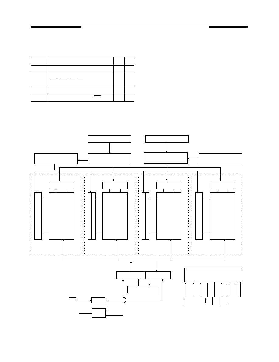
Block Diagram
Row decoder
Memory array
Bank 0
4096 x 256
x 16 bit
C
o
l
u
mn
dec
oder
S
ens
e
ampl
i
f
i
e
r
&
I(
O
)
bus
Row decoder
Memory array
Bank 1
4096 x 256
x 16 bit
C
o
l
u
mn d
e
c
o
der
S
e
ns
e
ampl
i
f
i
e
r
&
I(
O
)
bus
Row decoder
Memory array
Bank 2
4096 x 256
x 16 bit
Co
l
u
m
n
d
e
c
o
d
e
r
S
ens
e
ampl
i
f
i
e
r
&
I(
O
)
bus
Row decoder
Memory array
Bank 3
4096 x 256
x 16 bit
Co
l
u
m
n
d
e
c
o
d
e
r
S
ens
e ampl
i
f
i
e
r
&
I
(
O
)
bus
Input buffer
Output buffer
I/Q
0
-IQ
15
Column address
counter
Column address
buffer
Row address
buffer
Refresh Counter
A0 - A11, BA0, BA1
A0 - A7, AP, BA0, BA1
Control logic & timing generator
CL
K
CK
E
CS
RA
S
CA
S
WE
UDM
Row Addresses
Column Addresses
DLL
Strobe
Gen.
Data Strobe
CLK, CLK
CL
K
LD
M
DQS
4
V58C365164S Rev. 2.0 January 2003
MOSEL VITELIC
V58C365164S
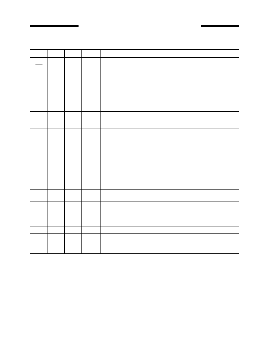
Signal Pin Description
Pin
Type
Signal
Polarity
Function
CLK
CLK
Input
Pulse
Positive
Edge
The system clock input. All inputs except DQs and DMs are sampled on the rising edge
of CLK.
CKE
Input
Level
Active High Activates the CLK signal when high and deactivates the CLK signal when low, thereby
initiates either the Power Down mode, Suspend mode, or the Self Refresh mode.
CS
Input
Pulse
Active Low CS enables the command decoder when low and disables the command decoder when
high. When the command decoder is disabled, new commands are ignored but previous
operations continue.
RAS, CAS
WE
Input
Pulse
Active Low When sampled at the positive rising edge of the clock, CAS, RAS, and WE define the
command to be executed by the SDRAM.
DQS
Input/
Output
Pulse
Active High Active on both edges for data input and output.
Center aligned to input data
Edge aligned to output data
A0 - A11
Input
Level
--
During a Bank Activate command cycle, A0-A11 defines the row address (RA0-RA11)
when sampled at the rising clock edge.
During a Read or Write command cycle, A0-An defines the column address (CA0-CAn)
when sampled at the rising clock edge.CAn depends from the SDRAM organization:
8M x 8 SDRAM CAn = CA8 (Page Length = 512 bits)
In addition to the column address, A10(=AP) is used to invoke autoprecharge operation
at the end of the burst read or write cycle. If A10 is high, autoprecharge is selected and
BA0, BA1 defines the bank to be precharged. If A10 is low, autoprecharge is disabled.
During a Precharge command cycle, A10(=AP) is used in conjunction with BA0 and BA1
to control which bank(s) to precharge. If A10 is high, all four banks will be precharged
simultaneously regardless of state of BA0 and BA1.
BA0,
BA1
Input
Level
--
Selects which bank is to be active.
DQx
Input/
Output
Level
--
Data Input/Output pins operate in the same manner as on conventional DRAMs.
DM
Input
Pulse
Active High In Write mode, DM has a latency of zero and operates as a word mask by allowing input
data to be written if it is low but blocks the write operation if is high.
VDD, VSS
Supply
Power and ground for the input buffers and the core logic.
VDDQ
VSSQ
Supply
--
--
Isolated power supply and ground for the output buffers to provide improved noise
immunity.
VREF
Input
Level
--
SSTL Reference Voltage for Inputs
5
V58C365164S Rev. 2.0 January 2003
MOSEL VITELIC
V58C365164S
Functional Description
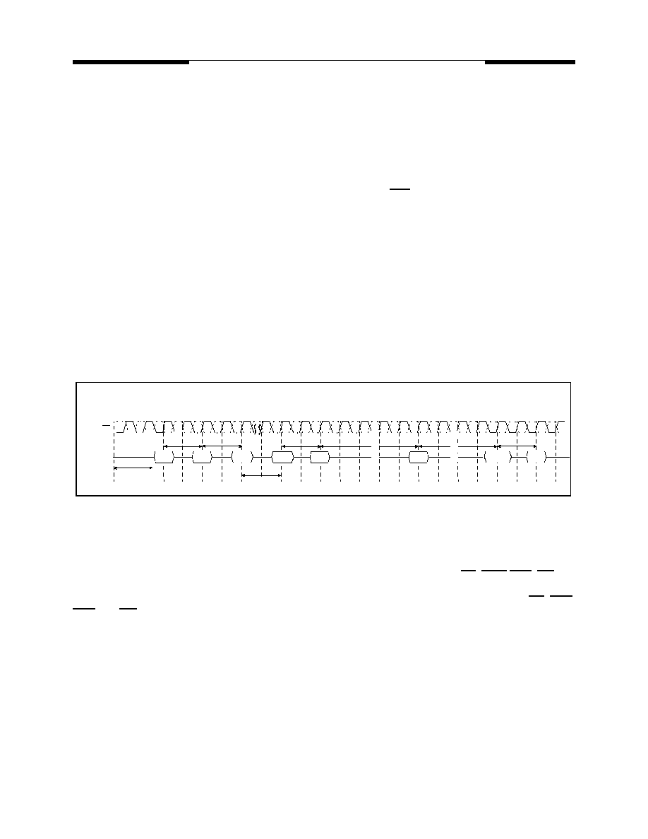
Power-Up Sequence
The following sequence is required for POWER UP.
1. Apply power and attempt to maintain CKE at a low state (all other inputs may be undefined.)
- Apply VDD before or at the same time as VDDQ.
- Apply VDDQ before or at the same time as VTT & Vref.
2. Start clock and maintain stable condition for a minimum of 200us.
3. The minimum of 200us after stable power and clock (CLK, CLK), apply NOP & take CKE high.
4. Precharge all banks.
5. Issue EMRS to enable DLL.(To issue "DLL Enable" command, provide "Low" to A0, "High" to BA0
and "Low" to all of the rest address pins, A1~A11 and BA1)
6. Issue a mode register set command for "DLL reset". The additional 200 cycles of clock input is
required to lock the DLL. (To issue DLL reset command, provide "High" to A8 and "Low" to BA0)
7. Issue precharge commands for all banks of the device.
8. Issue 2 or more auto-refresh commands.
9. Issue a mode register set command to initialize device operation.
Note1 Every "DLL enable" command resets DLL. Therefore sequence 6 can be skipped during power up. Instead of it,
the additional 200 cycles of clock input is required to lock the DLL after enabling DLL.
Extended Mode Register Set (EMRS)
The extended mode register stores the data for enabling or disabling DLL. The default value of the extend-
ed mode register is not defined, therefore the extended mode register must be written after power up for en-
abling or disabling DLL. The extended mode register is written by asserting low on CS, RAS, CAS, WE and
high on BA
0
(The DDR SDRAM should be in all bank precharge with CKE already high prior to writing into
the extended mode register). The state of address pins A
0
~ A
11
and BA
1
in the same cycle as CS, RAS,
CAS and WE low is written in the extended mode register. Two clock cycles are required to complete the
write operation in the extended mode register. The mode register contents can be changed using the same
command and clock cycle requirements during operation as long as all banks are in the idle state. A
0
is used
for DLL enable or disable. "High" on BA
0
is used for EMRS. All the other address pins except A
0
and BA
0
must be set to low for proper EMRS operation. A
1
is used at EMRS to indicate I/O strength A
1
= 0 full strength,
A
1
= 1 half strength. Refer to the table for specific codes.
Power up Sequence & Auto Refresh(CBR)
Command
0
1
2
3
4
5
6
7
8
9
10
11
12
13
14
15
16
17
18
19
t
RP
2 Clock min.
precharge
ALL Banks
2nd Auto
Refresh
Mode
Register Set
Any
Command
t
RFC
1st Auto
Refresh
t
RFC
min. 200 Cycle
∑ ∑
CK, CK
∑ ∑
∑ ∑
∑ ∑
∑ ∑
∑ ∑
∑ ∑
EMRS
MRS
2 Clock min.
200
µ
S Power up
to 1st command
DLL Reset
2 Clock min.
6
5
4
7
8
8
precharge
ALL Banks
∑ ∑
6
V58C365164S Rev. 2.0 January 2003
MOSEL VITELIC
V58C365164S
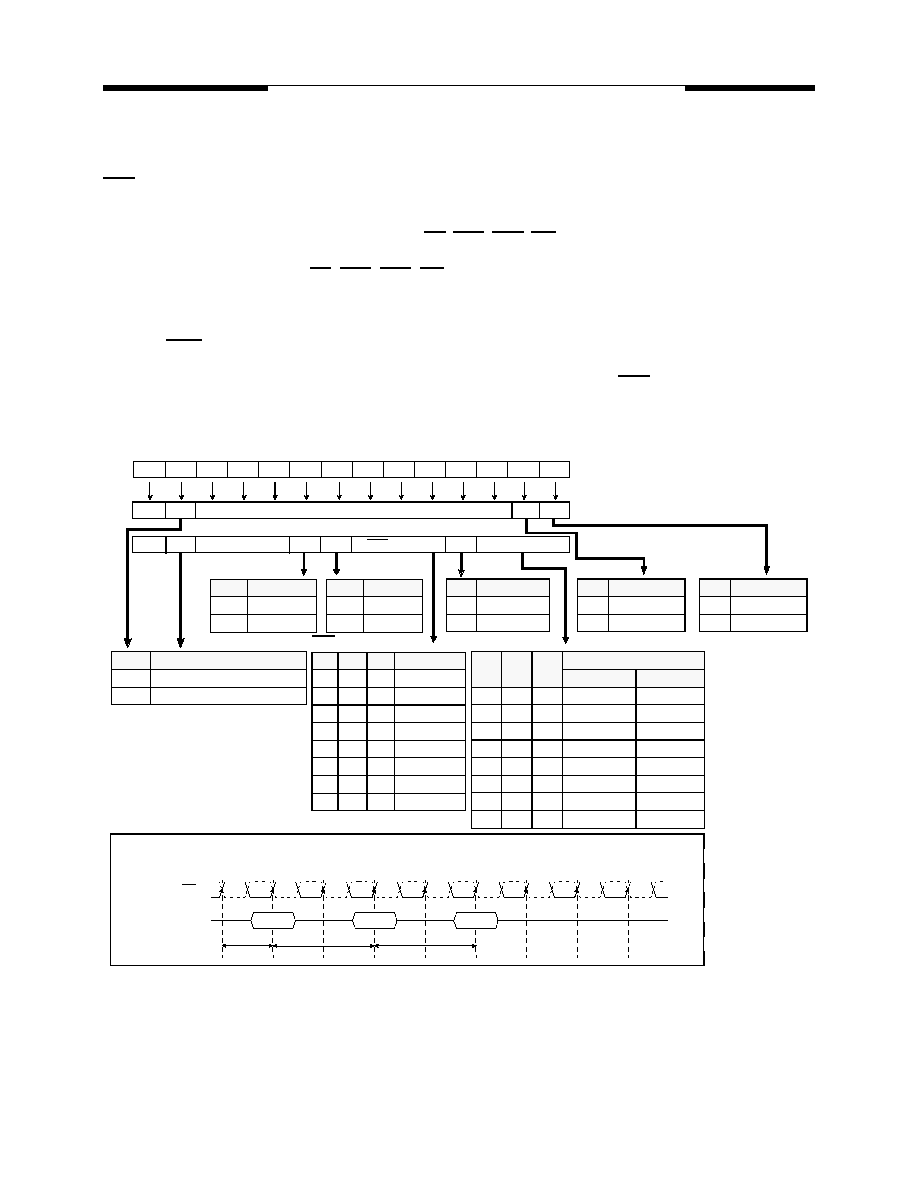
Mode Register Set (MRS)
The mode register stores the data for controlling the various operating modes of DDR SDRAM. It programs
CAS latency, addressing mode, burst length, test mode, DLL reset and various vendor specific options to
make DDR SDRAM useful for a variety of different applications. The default value of the mode register is not
defined, therefore the mode register must be written after EMRS setting for proper DDR SDRAM operation.
The mode register is written by asserting low on CS, RAS, CAS, WE and BA
0
(The DDR SDRAM should be
in all bank precharge with CKE already high prior to writing into the mode register). The state of address pins
A
0
~ A
11
in the same cycle as CS, RAS, CAS, WE and BA0 low is written in the mode register. Two clock
cycles are required to meet t
MRD
spec. The mode register contents can be changed using the same com-
mand and clock cycle requirements during operation as long as all banks are in the idle state. The mode reg-
ister is divided into various fields depending on functionality. The burst length uses A
0
~ A
2
, addressing mode
uses A
3
, CAS latency (read latency from column address) uses A
4
~ A
6
. A
7
is a Mosel Vitelic specific test
mode during production test. A
8
is used for DLL reset. A
7
must be set to low for normal MRS operation. Refer
to the table for specific codes for various burst length, addressing modes and CAS latencies.
1.
MRS can be issued only at all banks precharge state.
2.
Minimum tRP is required to issue MRS command.
Address Bus
CAS Latency
A
6
A
5
A
4
Latency
0
0
0
Reserve
0
0
1
Reserve
0
1
0
2
0
1
1
3
1
0
0
Reserve
Reserve
1
0
1
1
1
0
2.5
1
1
1
Reserve
Burst Length
A
2
A
1
A
0
Latency
Sequential
Interleave
0
0
0
Reserve
Reserve
0
0
1
2
2
0
1
0
4
4
0
1
1
8
8
1
0
0
Reserve
Reserve
1
0
1
Reserve
Reserve
1
1
0
Reserve
Reserve
1
1
1
Reserve
Reserve
A
7
mode
0
Normal
1
Test
A
3
Burst Type
0
Sequential
1
Interleave
* RFU(Reserved for future use)
should stay "0" during MRS
cycle.
A
8
DLL Reset
0
No
1
Yes
Mode Register Set
0
RFU : Must be set "0"
Extended Mode Register
Mode Register
DLL
I/O
A
0
DLL Enable
0
Enable
1
Disable
A
1
I/O Strength
0
Full
1
Half
BA
0
A
n
~ A
0
0
(Existing)MRS Cycle
1
Extended Funtions(EMRS)
Command
2
0
1
5
3
4
8
6
7
CK, CK
t
CK
t
MRD
Precharge
All Banks
Mode
Register Set
t
RP
*2
*1
Any
Command
BA
1
BA
0
A
11
A
10
A
9
A
8
A
7
A
6
A
5
A
4
A
3
A
2
A
1
A
0
0
TM
CAS Latency
BT
Burst Length
RFU
DLL
MRS
MRS

7
V58C365164S Rev. 2.0 January 2003
MOSEL VITELIC
V58C365164S
Mode Register Set Timing
Burst Mode Operation
Burst Mode Operation is used to provide a constant flow of data to memory locations (Write cycle), or from
memory locations (Read cycle). Two parameters define how the burst mode will operate: burst sequence and
burst length. These parameters are programmable and are determined by address bits A
0
--A
3
during the
Mode Register Set command. Burst type defines the sequence in which the burst data will be delivered or
stored to the SDRAM. Two types of burst sequence are supported: sequential and interleave. The burst
length controls the number of bits that will be output after a Read command, or the number of bits to be input
after a Write command. The burst length can be programmed to values of 2, 4, or 8. See the Burst Length
and Sequence table below for programming information.
Burst Length and Sequence
Burst Length
Starting Length (A
2
, A
1
, A
0
)
Sequential Mode
Interleave Mode
2
xx0
0, 1
0, 1
xx1
1, 0
1, 0
4
x00
0, 1, 2, 3
0, 1, 2, 3
x01
1, 2, 3, 0
1, 0, 3, 2
x10
2, 3, 0, 1
2, 3, 0, 1
x11
3, 0, 1, 2
3, 2, 1, 0
8
000
0,1, 2, 3, 4, 5, 6, 7
0,1, 2, 3, 4, 5, 6, 7
001
1, 2, 3, 4, 5, 6, 7, 0
1, 0, 3, 2, 5, 4, 7, 6
010
2, 3, 4, 5, 6, 7, 0, 1
2, 3, 0, 1, 6, 7, 4, 5
011
3, 4, 5, 6, 7, 0, 1, 2
3, 2, 1, 0, 7, 6, 5, 4
100
4, 5, 6, 7, 0, 1, 2, 3
4, 5, 6, 7, 0, 1, 2, 3
101
5, 6, 7, 0, 1, 2, 3, 4
5, 4, 7, 6, 1, 0, 3, 2
110
6, 7, 0, 1, 2, 3, 4, 5, 6
6, 7, 4, 5, 2, 3, 0, 1
111
7, 0, 1, 2, 3, 4, 5, 6
7, 6, 5, 4, 3, 2, 1, 0
T5
T0
T1
T2
T3
T4
T6
T7
T8
t
RP
t
MRD
t
CK
Pre- All
MRS/EMRS
ANY
Mode Register set (MRS) or Extended Mode Register Set (EMRS) can be issued only when all banks are in the idle state.
CK, CK
Command
If a MRS command is issued to reset the DLL, then an additional 200 clocks must occur prior to issuing any new command
T9
to allow time for the DLL to lock onto the clock.

8
V58C365164S Rev. 2.0 January 2003
MOSEL VITELIC
V58C365164S
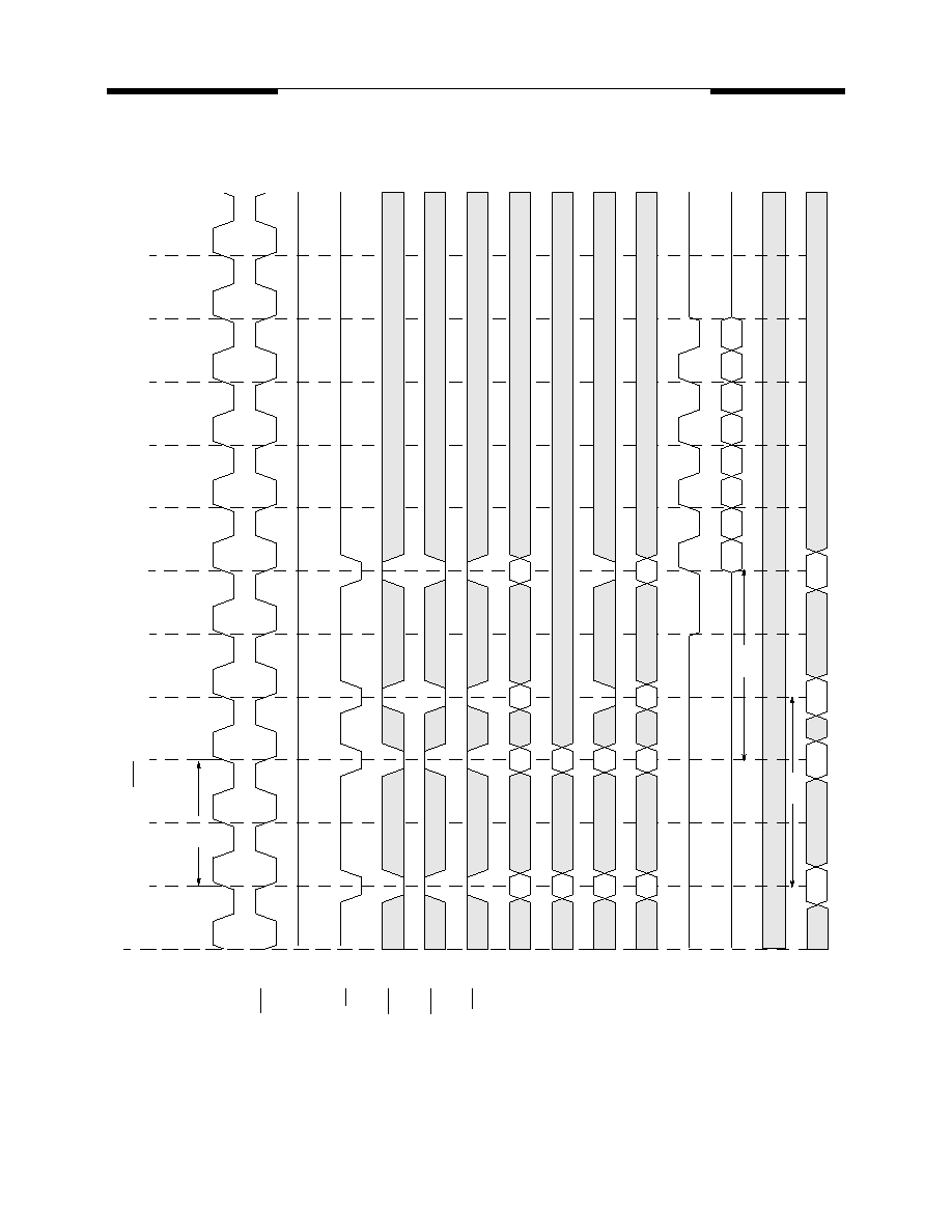
Bank Activate Command
The Bank Activate command is issued by holding CAS and WE high with CS and RAS low at the rising
edge of the clock. The DDR SDRAM has four independent banks, so two Bank Select addresses (BA
0
and
BA
1
) are supported. The Bank Activate command must be applied before any Read or Write operation can
be executed. The delay from the Bank Activate command to the first Read or Write command must meet or
exceed the minimum RAS to CAS delay time (t
RCD
min). Once a bank has been activated, it must be pre-
charged before another Bank Activate command can be applied to the same bank. The minimum time interval
between interleaved Bank Activate commands (Bank A to Bank B and vice versa) is the Bank to Bank delay
time (t
RRD
min).
Bank Activation Timing
Read Operation
With the DLL enabled, all devices operating at the same frequency within a system are ensured to have
the same timing relationship between DQ and DQS relative to the CK input regardless of device density, pro-
cess variation, or technology generation.
The data strobe signal (DQS) is driven off chip simultaneously with the output data (DQ) during each read
cycle. The same internal clock phase is used to drive both the output data and data strobe signal off chip to
minimize skew between data strobe and output data. This internal clock phase is nominally aligned to the
input differential clock (CK, CK) by the on-chip DLL. Therefore, when the DLL is enabled and the clock fre-
quency is within the specified range for proper DLL operation, the data strobe (DQS), output data (DQ), and
the system clock (CK) are all nominally aligned.
Since the data strobe and output data are tightly coupled in the system, the data strobe signal may be delayed
and used to latch the output data into the receiving device. The tolerance for skew between DQS and DQ
(t
DQSQ
) is tighter than that possible for CK to DQ (t
AC
) or DQS to CK (t
DQSCK
).
T0
T1
T2
T3
Tn
Tn+1
Tn+2
Tn+3
Tn+4
Tn+5
(CAS Latency = 2; Burst Length = Any)
t
RRD
(min)
t
RP
(min)
t
RC
t
RCD
(min)
Begin Precharge Bank A
CK, CK
BA/Address
Command
Bank/Col
Read/A
Bank/Row
Activate/A
Activate/B
Pre/A
Bank/Row
Activate/A
Bank
Bank/Row
t
RAS
(min)

9
V58C365164S Rev. 2.0 January 2003
MOSEL VITELIC
V58C365164S
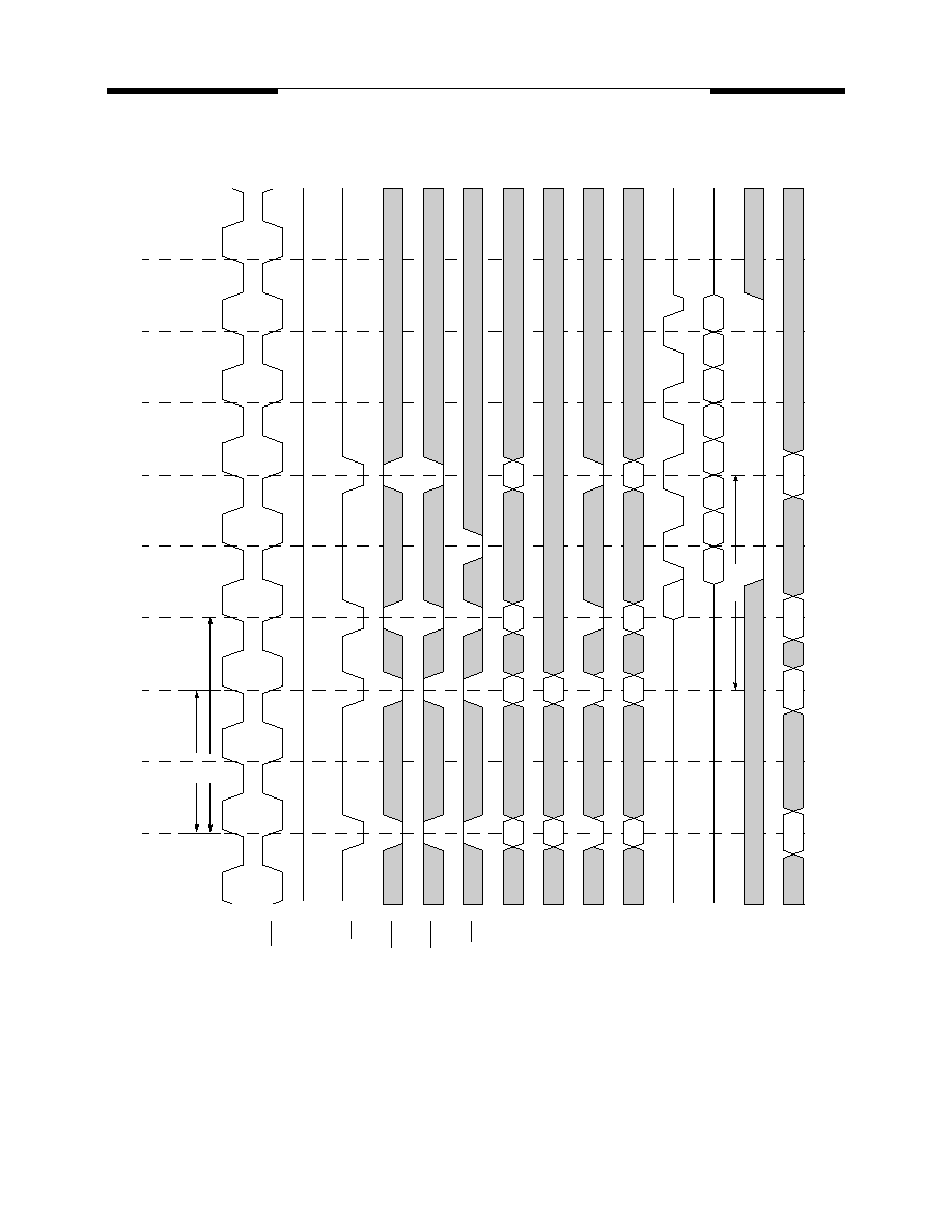
Output Data (DQ) and Data Strobe (DQS) Timing Relative to the Clock (CK)
During Read Cycles
The minimum time during which the output data (DQ) is valid is critical for the receiving device (i.e., a mem-
ory controller device). This also applies to the data strobe during the read cycle since it is tightly coupled to
the output data. The minimum data output valid time (t
DV
) and minimum data strobe valid time (t
DQSV
) are de-
rived from the minimum clock high/low time minus a margin for variation in data access and hold time due to
DLL jitter and power supply noise.
(CAS Latency = 2.5; Burst Length = 4)
T0
T1
T2
T3
T4
NOP
NOP
NOP
D
0
CK, CK
Command
DQS
DQ
D
2
t
DQSCK
(max)
t
DQSCK
(min)
D
1
t
AC
(min)
t
AC
(max)
D
3
READ
NOP

10
V58C365164S Rev. 2.0 January 2003
MOSEL VITELIC
V58C365164S
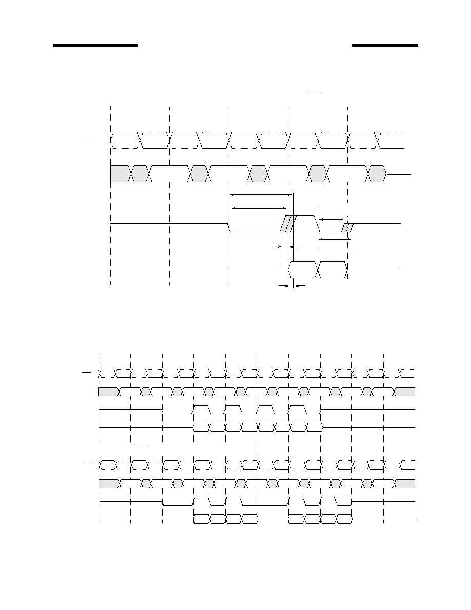
Output Data and Data Strobe Valid Window for DDR Read Cycles
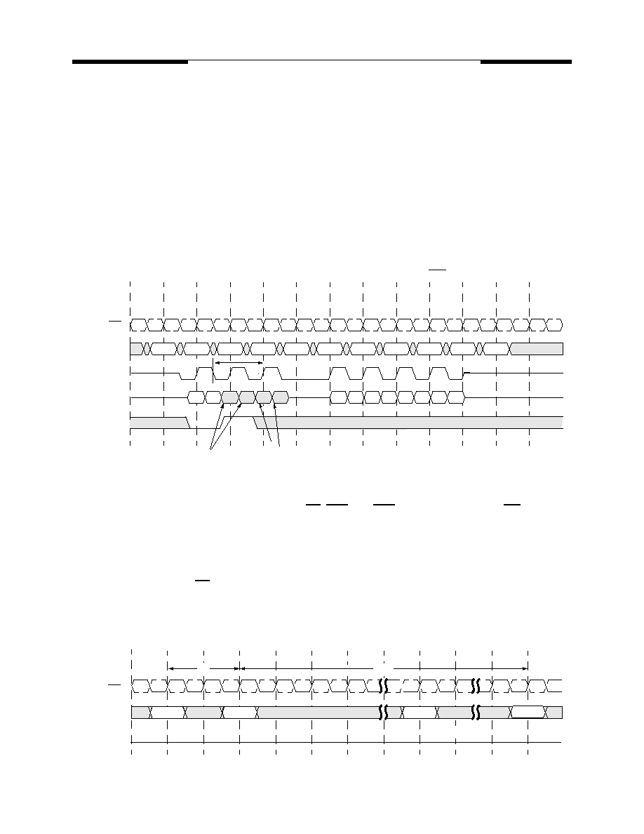
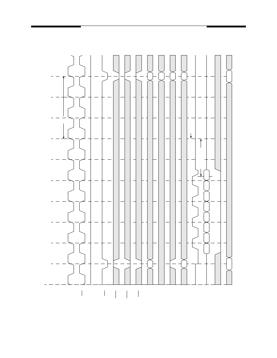
Read Preamble and Postamble Operation
Prior to a burst of read data and given that the controller is not currently in burst read mode, the data strobe
signal (DQS), must transition from Hi-Z to a valid logic low. The is referred to as the data strobe "read pream-
ble" (t
RPRE
). This transition from Hi-Z to logic low nominally happens one clock cycle prior to the first edge of
valid data.
Once the burst of read data is concluded and given that no subsequent burst read operations are initiated,
the data strobe signal (DQS) transitions from a logic low level back to Hi-Z. This is referred to as the data
strobe "read postamble" (t
RPST
). This transition happens nominally one-half clock period after the last edge of
valid data.
Consecutive or "gapless" burst read operations are possible from the same DDR SDRAM device with no
requirement for a data strobe "read" preamble or postamble in between the groups of burst data. The data
strobe read preamble is required before the DDR device drives the first output data off chip. Similarly, the
data strobe postamble is initiated when the device stops driving DQ data at the termination of read burst cy-
cles.
D
0
D
1
(CAS Latency = 2; Burst Length = 2)
T0
T1
T2
T3
T4
READ
NOP
NOP
NOP
Command
DQS
DQ
t
DV
(min)
CK, CK
t
DQSV
(min)
11
V58C365164S Rev. 2.0 January 2003
MOSEL VITELIC
V58C365164S
Data Strobe Preamble and Postamble Timings for DDR Read Cycles
Consecutive Burst Read Operation and Effects on the Data Strobe Preamble and Postamble
(CAS Latency = 2; Burst Length = 2)
T0
T1
T2
T3
T4
READ
NOP
NOP
NOP
D
0
D
1
CK, CK
Command
DQS
DQ
t
RPRE
(max)
t
RPST
(min)
t
RPRE
(min)
t
RPST
(max)
t
DQSQ
(max)
t
DQSQ
(min)
NOP
Read
B
NOP
NOP
NOP
NOP
Read
A
D0
A
D1
A
NOP
D2
A
D3
A
Command
DQS
DQ
Burst Read Operation (CAS Latency = 2; Burst Length = 4)
CK, CK
NOP
D0
B
D1
B
D2
B
D3
B
NOP
Read
B
NOP
NOP
NOP
NOP
Read
A
D0
A
D1
A
NOP
D2
A
D3
A
Command
DQS
DQ
Burst Read Operation (CAS Latency = 2; Burst Length = 4)
CK, CK
NOP
D0
B
D1
B
D2
B
D3
B
12
V58C365164S Rev. 2.0 January 2003
MOSEL VITELIC
V58C365164S
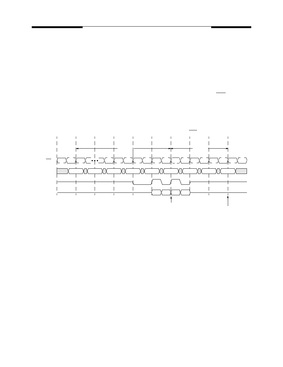
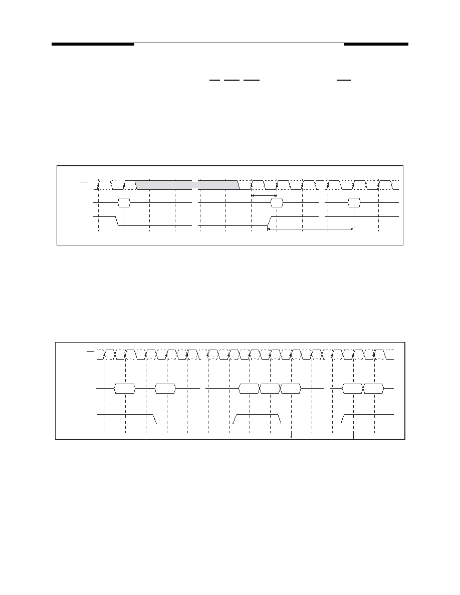
Auto Precharge Operation
The Auto Precharge operation can be issued by having column address A
10
high when a Read or Write
command is issued. If A
10
is low when a Read or Write command is issued, then normal Read or Write burst
operation is executed and the bank remains active at the completion of the burst sequence. When the Auto
Precharge command is activated, the active bank automatically begins to precharge at the earliest possible
moment during the Read or Write cycle once t
RAS
(min) is satisfied.
Read with Auto Precharge
If a Read with Auto Precharge command is initiated, the DDR SDRAM will enter the precharge operation
N-clock cycles measured from the last data of the burst read cycle where N is equal to the CAS latency pro-
grammed into the device. Once the autoprecharge operation has begun, the bank cannot be reactivated until
the minimum precharge time (t
RP
) has been satisfied.
Read with Autoprecharge Timing
(CAS Latency = 2; Burst Length = 4)
T0
T1
T2
T3
T4
T5
T6
T7
T8
D
0
D
1
D
2
D
3
Begin Autoprecharge
NOP
BA
R w/AP
NOP
NOP
NOP
NOP
NOP
BA
CK, CK
Command
DQS
DQ
t
RAS
(min)
t
RP
(min)
Earliest Bank A reactivate
T9

13
V58C365164S Rev. 2.0 January 2003
MOSEL VITELIC
V58C365164S
Read with Autoprecharge Timing as a Function of CAS Latency
T0
T1
T2
T3
T4
T5
T6
T7
T8
Begin Autoprecharge
NOP
RAP
NOP
NOP
NOP
NOP
BA
NOP
CK, CK
Command
DQS
DQ
t
RAS
(min)
t
RP
(min)
BA
NOP
T9
D
0
D
1
D
2
D
3
DQS
DQ
DQS
DQ
CAS Latency=2
CAS Latency=2.5
CAS Latency=3
(CAS Latency = 2, 2.5, 3; Burst Length = 4)
D
0
D
1
D
2
D
3
D
0
D
1
D
2
D
3

14
V58C365164S Rev. 2.0 January 2003
MOSEL VITELIC
V58C365164S
Precharge Timing During Read Operation
For the earliest possible Precharge command without interrupting a Read burst, the Precharge command
may be issued on the rising clock edge which is CAS latency (CL) clock cycles before the end of the Read
burst. A new Bank Activate (BA) command may be issued to the same bank after the RAS precharge time
(t
RP
). A Precharge command can not be issued until t
RAS
(min) is satisfied.
Read with Precharge Timing as a Function of CAS Latency
T0
T1
T2
T3
T4
T5
T6
T7
T8
D
0
D
1
D
2
D
3
NOP
Read
NOP
NOP
Pre
A
NOP
BA
NOP
CK, CK
Command
DQS
DQ
t
RAS
(min)
t
RP
(min)
BA
NOP
T9
D
0
D
1
D
2
D
3
DQS
DQ
D
0
D
1
D
2
D
3
DQS
DQ
CAS Latency=2
CAS Latency=2.5
CAS Latency=3
(CAS Latency = 2, 2.5, 3; Burst Length = 4)

15
V58C365164S Rev. 2.0 January 2003
MOSEL VITELIC
V58C365164S
Burst Stop Command
The Burst Stop command is valid only during burst read cycles and is initiated by having RAS and CAS
high with CS and WE low at the rising edge of the clock. When the Burst Stop command is issued during a
burst Read cycle, both the output data (DQ) and data strobe (DQS) go to a high impedance state after a delay
(L
BST
) equal to the CAS latency programmed into the device. If the Burst Stop command is issued during a
burst Write cycle, the command will be treated as a NOP command.
Read Terminated by Burst Stop Command Timing
(CAS Latency = 2, 2.5, 3; Burst Length = 4)
T0
T1
T2
T3
T4
T5
T6
BST
NOP
NOP
NOP
NOP
Read
D
0
D
1
CK, CK
Command
DQS
DQ
D
0
D
1
DQS
DQ
D
0
D
1
DQS
DQ
CAS Latency = 2
CAS Latency = 2.5
CAS Latency = 3
L
BST
L
BST
L
BST

16
V58C365164S Rev. 2.0 January 2003
MOSEL VITELIC
V58C365164S
Read Interrupted by a Precharge
A Burst Read operation can be interrupted by a precharge of the same bank. The Precharge command to
Output Disable latency is equivalent to the CAS latency.
Read Interrupted by a Precharge Timing
Burst Write Operation
The Burst Write command is issued by having CS, CAS, and WE low while holding RAS high at the rising
edge of the clock. The address inputs determine the starting column address. The memory controller is re-
quired to provide an input data strobe (DQS) to the DDR SDRAM to strobe or latch the input data (DQ) and
data mask (DM) into the device. During Write cycles, the data strobe applied to the DDR SDRAM is required
to be nominally centered within the data (DQ) and data mask (DM) valid windows. The data strobe must be
driven high nominally one clock after the write command has been registered. Timing parameters t
DQSS
(min)
and t
DQSS
(max) define the allowable window when the data strobe must be driven high.
Input data for the first Burst Write cycle must be applied one clock cycle after the Write command is regis-
tered into the device (WL=1). The input data valid window is nominally centered around the midpoint of the
data strobe signal. The data window is defined by DQ to DQS setup time (t
QDQSS
) and DQ to DQS hold time
(t
QDQSH
). All data inputs must be supplied on each rising and falling edge of the data strobe until the burst
length is completed. When the burst has finished, any additional data supplied to the DQ pins will be ignored.
Write Preamble and Postamble Operation
Prior to a burst of write data and given that the controller is not currently in burst write mode, the data strobe
signal (DQS), must transition from Hi-Z to a valid logic low. This is referred to as the data strobe "write preamble".
This transition from Hi-Z to logic low nominally happens on the falling edge of the clock after the write com-
mand has been registered by the device. The preamble is explicitly defined by a setup time (t
WPRES
(min)) and
hold time (t
WPREH
(min)) referenced to the first falling edge of CK after the write command.
T0
T1
T2
T3
T4
T5
T6
T7
T8
D
0
D
1
D
2
D
3
NOP
Read
NOP
NOP
Pre
A
NOP
BA
NOP
CK, CK
Command
DQS
DQ
t
RAS
(min)
t
RP
(min)
BA
NOP
T9
D
0
D
1
D
2
D
3
DQS
DQ
D
0
D
1
D
2
D
3
DQS
DQ
CAS Latency=2
CAS Latency=2.5
CAS Latency=3
(CAS Latency = 2, 2.5, 3; Burst Length = 8)

17
V58C365164S Rev. 2.0 January 2003
MOSEL VITELIC
V58C365164S
Burst Write Timing
Once the burst of write data is concluded and given that no subsequent burst write operations are initiated,
the data strobe signal (DQS) transitions from a logic low level back to Hi-Z. This is referred to as the data
strobe "write postamble". This transition happens nominally one-half clock period after the last data of the
burst cycle is latched into the device.
(CAS Latency = Any; Burst Length = 4)
T0
T1
T2
T3
T4
WRITE
NOP
NOP
NOP
D
0
D
1
D
2
D
3
CK, CK
Command
DQS(nom)
DQ(nom)
t
WPRES
t
WPREH
t
DQSS
t
WPST
t
QDQSH
D
0
D
1
D
2
D
3
DQS(min)
DQ(min)
t
DQSS
(min)
D
0
D
1
D
2
D
3
DQS(max)
DQ(max)
t
WPRES
(min)
t
DQSS
(max)
t
QDQSS
t
QDQSS
t
QDQSH
t
WPREH
(min)
t
WPREH
(max)
t
WPRES
(max)
18
V58C365164S Rev. 2.0 January 2003
MOSEL VITELIC
V58C365164S
Write Interrupted by a Precharge
A Burst Write can be interrupted before completion of the burst by a Precharge command, with the only
restriction being that the interval that separates the commands be at least one clock cycle.
Write Interrupted by a Precharge Timing
Write with Auto Precharge
If A
10
is high when a Write command is issued, the Write with auto Precharge function is performed. Any
new command to the same bank should not be issued until the internal precharge is completed. The internal
precharge begins after keeping t
WR
(min.).
Write with Auto Precharge Timing
(CAS Latency = 2; Burst Length = 8)
T0
T1
T2
T3
T4
T5
T6
T7
T8
T9
T10
T11
Write
A
NOP
Pre
A
NOP
NOP
NOP
NOP
NOP
NOP
NOP
NOP
CK, CK
Command
DQS
T12
DM
D
0
D
1
D
2
D
3
DQ
Data is masked
by Precharge Command
Data is masked
by DM input
DQS input ignored
D
4
D
5
t
WR
(CAS Latency = Any; Burst Length = 4)
T0
T1
T2
T3
T4
T5
T6
T7
T8
D
0
D
1
D
2
D
3
NOP
WAP
NOP
NOP
NOP
NOP
NOP
NOP
BA
CK, CK
Command
DQS
DQ
t
RAS
(min)
t
RP
(min)
BA
NOP
T9
T10
t
WR
(min)
Begin Autoprecharge
19
V58C365164S Rev. 2.0 January 2003
MOSEL VITELIC
V58C365164S
Precharge Timing During Write Operation
Precharge timing for Write operations in DRAMs requires enough time to satisfy the write recovery require-
ment. This is the time required by a DRAM sense amp to fully store the voltage level. For DDR SDRAMs, a
timing parameter (t
WR
) is used to indicate the required amount of time between the last valid write operation
and a Precharge command to the same bank.
The "write recovery" operation begins on the rising clock edge after the last DQS edge that is used to strobe
in the last valid write data. "Write recovery" is complete on the next rising clock edge that is used to strobe in
the Precharge command.
For the earliest possible Precharge command following a Write burst without interrupting the burst, the
minimum time for "write recovery" is 1.25 clock cycles. Maximum "write recovery" time is 1.75 clock cycles.
Write with Precharge Timing
(CAS Latency = Any; Burst Length = 4)
T0
T1
T2
T3
T4
T5
T6
T7
T8
D
0
D
1
D
2
D
3
NOP
Write
NOP
NOP
NOP
NOP
Pre
A
NOP
CK, CK
Command
DQS
DQ
t
RAS
(min)
t
RP
(min)
BA
NOP
T9
T10
t
WR
(min)
D
0
D
1
D
2
D
3
DQS
DQ
t
WR
(max)
BA

20
V58C365164S Rev. 2.0 January 2003
MOSEL VITELIC
V58C365164S
Data Mask Function
The DDR SDRAM has a Data Mask function that is used in conjunction with the Write cycle, but not the
Read cycle. When the Data Mask is activated (DM high) during a Write operation, the Write is blocked (Mask
to Data Latency = 0).
When issued, the Data Mask must be referenced to both the rising and falling edges of Data Strobe.
Data Mask Timing
Burst Interruption
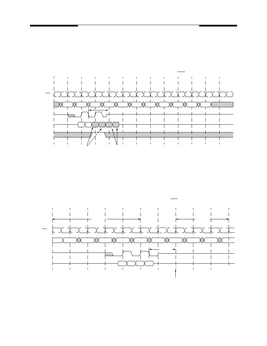
Read Interrupted by a Read
A Burst Read can be interrupted before completion of the burst by issuing a new Read command to any
bank. When the previous burst is interrupted, the remaining addresses are overridden with a full burst length
starting with the new address. The data from the first Read command continues to appear on the outputs until
the CAS latency from the interrupting Read command is satisfied. At this point, the data from the interrupting
Read command appears on the bus. Read commands can be issued on each rising edge of the system clock.
It is illegal to interrupt a Read with autoprecharge command with a Read command.
Read Interrupted by a Read Command Timing
(CAS Latency = Any; Burst Length = 8)
T0
T1
T2
T3
T4
T5
T6
T7
T8
D
0
D
1
D
2
D
3
D
4
D
5
D
6
D
7
NOP
NOP
NOP
NOP
NOP
NOP
NOP
Write
CK, CK
Command
DQS
DQ
DM
T9
t
DMDQSS
t
DMDQSS
t
DMDQSH
t
DMDQSH
(CAS Latency = 2; Burst Length = 4)
T0
T1
T2
T3
T4
T5
T6
T7
T8
Read
B
NOP
NOP
NOP
NOP
NOP
NOP
DA0 DA1 DB0 DB1
Read
A
DB2 DB3
CK, CK
Command
DQS
DQ
T9

21
V58C365164S Rev. 2.0 January 2003
MOSEL VITELIC
V58C365164S
Read Interrupted by a Write
To interrupt a Burst Read with a Write command, a Burst Stop command must be asserted to stop the burst
read operation and 3-state the DQ bus. Additionally, control of the DQS bus must be turned around to allow
the memory controller to drive the data strobe signal (DQS) into the DDR SDRAM for the write cycles. Once
the Burst Stop command has been issued, a Write command can not be issued until a minimum delay or
latency (L
BST
) has been satisfied. This latency is measured from the Burst Stop command and is equivalent
to the CAS latency programmed into the mode register. In instances where CAS latency is measured in half
clock cycles, the minimum delay (L
BST
) is rounded up to the next full clock cycle (i.e., if CL=2 then L
BST
=2, if
CL=2.5 then L
BST
=3). It is illegal to interrupt a Read with autoprecharge command with a Write command.
Read Interrupted by Burst Stop Command Followed by a Write Command Timing
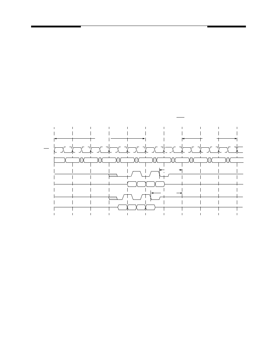
Write Interrupted by a Write
A Burst Write can be interrupted before completion by a new Write command to any bank. When the pre-
vious burst is interrupted, the remaining addresses are overridden with a full burst length starting with the new
address. The data from the first Write command continues to be input into the device until the Write Latency
of the interrupting Write command is satisfied (WL=1) At this point, the data from the interrupting Write com-
mand is input into the device. Write commands can be issued on each rising edge of the system clock. It is
illegal to interrupt a Write with autoprecharge command with a Write command.
Write Interrupted by a Write Command Timing
(CAS Latency = 2; Burst Length = 4)
T0
T1
T2
T3
T4
T5
T6
T7
T8
BST
NOP
Write
NOP
NOP
NOP
NOP
D
0
D
1
Read
D
0
D
1
D
2
D
3
CK, CK
Command
DQS
DQ
T9
L
BST
(CAS Latency = Any; Burst Length = 4)
T0
T1
T2
T3
T4
T5
T6
T7
T8
Write
A
NOP
NOP
Write
B
NOP
NOP
NOP
NOP
DA0 DA1 DB0 DB1 DB2 DB3
CK, CK
Command
DQS
DQ
DM
T9
Write Latency
DM0 DM1 DM0 DM1 DM2 DM3
22
V58C365164S Rev. 2.0 January 2003
MOSEL VITELIC
V58C365164S
Write Interrupted by a Read
A Burst Write can be interrupted by a Read command to any bank. If a burst write operation is interrupted
prior to the end of the burst operation, then the last two pieces of input data prior to the Read command must
be masked off with the data mask (DM) input pin to prevent invalid data from being written into the memory
array. Any data that is present on the DQ pins coincident with or following the Read command will be masked
off by the Read command and will not be written to the array. The memory controller must give up control of
both the DQ bus and the DQS bus at least one clock cycle before the read data appears on the outputs in
order to avoid contention. In order to avoid data contention within the device, a delay is required (t
CDLR
) from
the last valid data input before a Read command can be issued to the device. It is illegal to interrupt a Write
with autoprecharge command with a Read command.
Write Interrupted by a Read Command Timing
Auto Refresh
The Auto Refresh command is issued by having CS, RAS, and CAS held low with CKE and WE high at the
rising edge of the clock. All banks must be precharged and idle for a t
RP
(min) before the Auto Refresh com-
mand is applied. No control of the address pins is required once this cycle has started because of the internal
address counter. When the Auto Refresh cycle has completed, all banks will be in the idle state. A delay be-
tween the Auto Refresh command and the next Activate command or subsequent Auto Refresh command
must be greater than or equal to the t
RFC
(min). Commands may not be issued to the device once an Auto
Refresh cycle has begun. CS input must remain high during the refresh period or NOP commands must be
registered on each rising edge of the CK input until the refresh period is satisfied.
Auto Refresh Timing
(CAS Latency = 2; Burst Length = 8)
T0
T1
T2
T3
T4
T5
T6
T7
T8
T9
T10
T11
Write
NOP
Read
NOP
NOP
NOP
NOP
NOP
NOP
NOP
NOP
CK, CK
Command
DQS
T12
DM
D
2
D
3
D
4
D
5
D
0
D
2
D
3
D
4
D
5
D
6
D
1
D
7
DQ
Data is masked
by Read command
Data is masked
by DM input
DQS input ignored
D
0
D
1
t
CDLR
T0
T1
T2
T3
T4
T5
T6
T7
T8
T9
T10
NOP
CK, CK
Command
CKE
T11
Auto Ref
ANY
High
Pre All
t
RFC
t
RP
23
V58C365164S Rev. 2.0 January 2003
MOSEL VITELIC
V58C365164S
Self Refresh
A self refresh command is defined by having CS, RAS, CAS and CKE held low with WE high at the rising
edge of the clock (CK). Once the self refresh command is initiated, CKE must be held low to keep the device
in self refresh mode. During the self refresh operation, all inputs except CKE are ignored. The clock is inter-
nally disabled during self refresh operation to reduce power consumption. The self refresh is exited by sup-
plying stable clock input before returning CKE high, asserting deselect or NOP command and then asserting
CKE high for longer than t
SREX
for locking of DLL. The auto refresh is required before self refresh entry and
after self refresh exit.
Power Down Mode
The power down mode is entered when CKE is low and exited when CKE is high. Once the power down
mode is initiated, all of the receiver circuits except clock, CKE and DLL circuit tree are gated off to reduce
power consumption. All banks should be in idle state prior to entering the precharge power down mode and
CKE should be set high at least 1tck+tIS prior to row active command. During power down mode, refresh
operations cannot be performed, therefore the device cannot remain in power down mode longer than the
refresh period (t
REF
) of the device.
Command
CKE
Stable Clock
t
SREX
Auto
Refresh
NOP
Self
Refresh
∑ ∑
∑ ∑
∑ ∑
∑ ∑
∑ ∑
∑ ∑
CK, CK
∑ ∑
CKE
Precharge
Active
Read
NOP
Active
power down
power down
Exit
Active
Entry
power
Exit
down
power
Entry
down
Precharge
∑ ∑
∑ ∑
∑ ∑
∑ ∑
∑ ∑
∑ ∑
precharge
Command
CK, CK

24
V58C365164S Rev. 2.0 January 2003
MOSEL VITELIC
V58C365164S
SSTL_2 Input AC/DC Logic Levels
Note: 1. The relationship of the V
DDQ
of the driving device and the V
REF
of the receiving device is what determines noise margins.
However, in the case of V
IH
(max) (input overdrive), it is the V
DDQ
of the receiving device that is referenced. In the case where
a device is implemented such that supports SSTL_2 inputs but has no SSTL_2 outputs (e.g., a translator), and therefore no
V
DDQ
supply voltage connection, inputs must tolerate input overdrive to 3.0V (High corner V
DDQ
+300mV.)
SSTL_2 AC Test Conditions
Notes: 1. Input waveform timing is referenced to the input signal crossing the V
REF
level applied to the device.
2. Compliant devices must still meet the V
IH
(AC) and V
IL
(AC) specifications under actual use conditions.
3. The 1 V/ns input signal minimum slew rate is to be maintained in the V
IL
max (AC) to V
IL
min (AC) range of the input
signal swing.
SSTL_2 Output Buffers
The input voltage provided to the receiver depends on three parameters:
V
DDQ
and current drive capabilities of the output buffer
Termination voltage
Termination resistance
V
DDQ
=2.5 + 0.2V
Class II SSTL_2 Output Buffer (Driver)
Symbol
Parameter
Min
Max
Units
Notes
V
IH
(DC)
DC Input Logic High
V
REF
+0.18
V
DDQ
+0.3
V
1
V
IH
(AC)
AC Input Logic High
V
REF
+0.35
--
V
V
IL
(DC)
DC Input Logic Low
≠0.30
V
REF
≠0.18
V
V
IL
(AC)
AC Input Logic Low
--
V
REF
≠0.35
V
Symbol
Parameter
Value
Units
Notes
V
REF
Input Reference Voltage
0.5*V
DDQ
V
1
V
SWING
(max)
Input Signal Maximum Peak to Peak Swing
1.5
V
1, 2
SLEW
Input Signal Minimum Slew Rate
1.0
V/ns
3
V
REF
V
IN
V
TT
= 0.5 *V
DDQ
C
LOAD
= 30pF
V
DDQ
V
SSQ
V
OUT
Receiver
RT=50
Output
Buffer

25
V58C365164S Rev. 2.0 January 2003
MOSEL VITELIC
V58C365164S
DC CHARACTERISTICS
Recommended operating conditions Unless Otherwise Noted, T
A
=0 to 70∞C
Parameter
Symbol
Test Condition
CAS
Latency
Version
Unit
-36
≠4
≠5
Operating Current
(One Bank Active)
I
CC
1
Burst Length=2 t
RC
=t
RC
(min) I
OL
=0mA
155
150
140
mA
Precharge Standby Current
in Power-Down Mode
I
CC2
P
CKE=V
IL
(max), t
CC
=10ns
20
mA
Precharge Standby Current
in Non Power-Down Mode
I
CC2
N
CKE=VIH(min), CS=VIH(min), tCC=10ns
Input signals are changed once during 20ns
45
mA
Active Standby Current in Power-
Down Mode
I
CC3
P
CKE=V
IL
(max), t
CC
=10ns
30
mA
Active Standby Current in Non-
Power-Down Mode
I
CC3
N
CKE=VIH(min), CS=VIH(min), tCC=10ns
Input signals are changed once during 20ns
60
mA
Operating Current (Burst Mode)
I
CC4
I
OL
=0mA
Page Burst
All Banks activated
t
CCD
=2CKs
3
165
160
150
mA
Refresh Current
I
CC5
t
RC
=t
RFC
(min)
200
mA
Self Refresh Current
I
CC6
CKE=0.2V
2
mA
26
V58C365164S Rev. 2.0 January 2003
MOSEL VITELIC
V58C365164S
AC Characteristics (T
A
=0 to +70∞C, V
CC
=3.3 ± 0.3V)
Symbol
Parameter
-36
≠4
≠5
Unit
Min.
Max.
Min.
Max.
Min.
Max.
Clock Cycle
t
CK
Clock Cycle
CL = 2.0
5.4
8
6
8
7.5
8
ns
CL = 2.5
4.3
8
4.8
8
6
8
ns
CL = 3.0
3.6
8
4
8
5
8
ns
t
CH
Clock Duty Cycle
0.45
0.55
0.45
0.55
0.45
0.55
%
t
CL
0.45
0.55
0.45
0.55
0.45
0.55
%
Command Cycle
t
RAS
Row Active Time (ACT->PRE)
36
100K
36
100K
40
100K
ns
t
RP
Row Precharge (PRE->ACT)
18
-
20
-
20
-
ns
t
RC
Row Cycle (ACT->ACT)
54
-
56
-
60
-
ns
t
RCD
RAS->CAS Delay (ACT->WR/RD)
18
-
18
-
20
-
ns
t
RRD
RAS->RAS Delay (ACTa->ACTb)
7.2
-
8
-
10
-
ns
t
RFC
Auto-Refresh (REF->REF/ACT)
68
-
68
-
70
-
ns
t
REF
Refresh Cycle
-
64
-
64
-
64
ms
t
SREX(DLL)
Self-Refresh Exit Delay
200
-
200
-
200
-
cycles
t
SREX
1
-
1
-
1
-
t
RC
t
IS
CMD, ADDR->CLK Setup
0.9
-
0.9
-
1.0
-
ns
t
IH
CMD, ADDR->CLK Hold
0.9
-
0.9
-
1.0
-
ns
t
CCD
CAS->CAS Delay (Cola->Colb)
1
1
1
t
CK
t
MRD
Mode Register Set Delay
3
3
2
t
CK
t
PDENT
Power Down Entry Delay
1
1
1
t
CK
t
PDEX(DLL)
Power Down Exit Delay
1
1
1
t
CK
t
PDEX
1
1
1
t
CK
Read Cycle
t
AC
CLK->DQ Skew
-0.1
0.2
-0.2
0.125
-0.2
0.1
t
CK
t
DQSCK
CLK->DQS Skew
-0.1
0.2
-0.2
0.125
-0.2
0.1
t
CK
t
DQSQ
DQS->DQ Skew
-0.075
0.1
-0.075
0.1
-0.075
0.08
t
CK
t
DV
DQ/DQS Valid Window
0.3
-
0.3
-
0.3
-
t
CK
t
RPRE
Read DQS Preamble
0.9
1.1
0.9
1.1
0.9
1.1
t
CK
t
RPST
Read DQS Postamble
0.4
0.6
0.4
0.6
0.4
0.6
t
CK

27
V58C365164S Rev. 2.0 January 2003
MOSEL VITELIC
V58C365164S
Write Cycle
t
WPRES
Write Preamble DQS Setup
0
-
0
-
0
-
t
CK
t
WPREH
Write Preamble DQS Hold
0.42
-
0.375
-
0.3
-
t
CK
t
DQSS
Write Preamble CLK->DQS (first)
0.8
1.25
0.8
1.25
0.75
1.25
t
CK
t
DSH
Write DQS High Width
0.4
0.6
0.4
0.6
0.4
0.6
t
CK
t
DSL
Write DQS Low Width
0.4
0.6
0.4
0.6
0.4
0.6
t
CK
t
WPST
Write Postamble DQS (last) -> Hi-Z
0.4
0.6
0.4
0.6
0.4
0.6
t
CK
t
DQSR
Write (last DIN) -> READ Command
2
-
2
-
1
-
t
CK
t
WR
Write (last DIN) -> PRE Command
3
-
2
-
2
-
t
CK
t
DS
DQ/DM -> DQS Setup (Data Setup)
0.25
-
0.25
-
0.25
-
t
CK
t
DH
DQ/DM -> DQS Hold (Data Hold)
0.25
-
0.25
-
0.25
-
t
CK
t
QDQSS
Date Input to Data Strobe Setup Time
0.075
-
0.075
-
0.075
-
t
CK
t
QDQSH
Date Input to Data Strobe Hold Time
0.075
-
0.075
-
0.075
-
t
CK
t
DMDSQS
Date Mask to Data Strobe Setup Time
0.075
-
0.075
-
0.075
-
t
CK
t
DMDQSH
Date Mask to Data Strobe Hold Time
0.075
-
0.075
-
0.075
-
t
CK
AC Characteristics (Continued) (T
A
=0 to +70∞C, V
CC
=3.3 ± 0.3V)
Symbol
Parameter
-36
≠4
≠5
Unit
Min.
Max.
Min.
Max.
Min.
Max.

28
V58C365164S Rev. 2.0 January 2003
MOSEL VITELIC
V58C365164S
Command
CKEn-1
CKEn
CS
RAS
CAS
WE
ADDR
A10/
AP
BA
Note
H
X
L
L
L
L
OP code
1,2
H
X
L
L
L
L
1,2
Device Deselect
H
X
H
X
X
X
X
1
No
L
H
H
H
Bank Active
H
X
L
L
H
H
RA
V
1
Read
H
X
L
H
L
H
CA
L
V
1
Read with Autoprecharge
H
1,3
Write
H
X
L
H
L
L
CA
L
V
1
Write with Autoprecharge
H
1,4
Precharge All Banks
H
X
L
L
H
L
X
H
X
1,5
Precharge selected Bank
L
V
1
Read Burst Stop
H
X
L
H
H
L
X
1
Auto
H
H
L
L
L
H
X
1
Self Refresh
Entry
H
L
L
L
L
H
X
1
Exit
L
H
H
X
X
X
1
L
H
H
H
Precharge Power
Down Mode
Entry
H
L
H
X
X
X
X
1
L
H
H
H
1
Exit
L
H
H
X
X
X
1
L
H
H
H
1
Active Power
Down Mode
Entry
H
L
H
X
X
X
X
1
L
V
V
V
1
Exit
L
H
X
1
Note :
1. LDM/UDM states are Don't Care. Refer to below Write Mask Truth Table.
2. OP Code(Operand Code) consists of A0~A11 and BA0~BA1 used for Mode Register setting duing Extended MRS or MRS.
Before entering Mode Register Set mode, all banks must be in a precharge state and MRS command can be issued after tRP
period from Prechagre command.
3. If a Read with Autoprecharge command is detected by memory component in CK(n), then there will be no command presented
to activated bank until CK(n+BL/2+tRP).
4. If a Write with Autoprecharge command is detected by memory component in CK(n), then there will be no command presented
to activated bank until CK(n+BL/2+1+tDPL+tRP). Last Data-In to Prechage delay(tDPL) which is also called Write Recovery Time
(tWR) is needed to guarantee that the last data has been completely written.
5. If A10/AP is High when Precharge command being issued, BA0/BA1 are ignored and all banks are selected to be
precharged.
( H=Logic High Level, L=Logic Low Level, X=Don't Care, V=Valid Data Input, OP Code=Operand Code, NOP=No Operation )
OP code
Refresh
Operation
Mode Register Set
Extended Mode Register Set
DDR SDRAM SIMPLIFIED COMMAND TRUTH TABLE

29
V58C365164S Rev. 2.0 January 2003
MOSEL VITELIC
V58C365164S
Complete List of Operation Commands
DDR SDRAM Function Truth Table
CURRENT
STATE
1
CS
RAS
CAS
WE
BS
Addr
ACTION
Idle
H
L
L
L
L
L
L
L
X
H
H
H
L
L
L
L
X
H
H
L
H
H
L
L
X
H
L
X
H
L
H
L
X
X
BS
BS
BS
BS
X
Op-
X
X
X
X
RA
AP
X
Code
NOP or Power Down
NOP
ILLEGAL
2
ILLEGAL
2
Row (&Bank) Active; Latch Row Address
NOP
4
Auto-Refresh or Self-Refresh
5
Mode reg. Access
5
Row Active
H
L
L
L
L
L
L
X
H
H
H
L
L
L
X
H
L
L
H
H
L
X
X
H
L
H
L
X
X
X
BS
BS
BS
BS
X
X
X
CA,AP
CA,AP
X
AP
X
NOP
NOP
Begin Read; Latch CA; DetermineAP
Begin Write; Latch CA; DetermineAP
ILLEGAL
2
Precharge
ILLEGAL
Read
H
L
L
L
L
L
L
L
X
H
H
H
H
L
L
L
X
H
H
L
L
H
H
L
X
H
L
H
L
H
L
X
X
X
BS
BS
BS
BS
BS
X
X
X
X
CA,AP
CA,AP
X
AP
X
NOP (Continue Burst to End;>Row Active)
NOP (Continue Burst to End;>Row Active)
Term Burst
Term Burst, New Read, DetermineAP
3
ILLEGAL (Need Term Burst before Write)
ILLEGAL to Same Bank, other Bank 0K if tRRD is Satisfied
Term Burst, Precharge
ILLEGAL
Write
H
L
L
L
L
L
L
L
X
H
H
H
H
L
L
L
X
H
H
L
L
H
H
L
X
H
L
H
L
H
L
X
X
X
BS
BS
BS
BS
BS
X
X
X
X
CA,AP
CA,AP
X
AP
X
NOP (Continue Burst to End;>Row Active)
NOP (Continue Burst to End;>Row Active)
NOP
Term Burst, Start Read, DetermineAP
3
Term Burst, New Write, DetermineAP
3
ILLEGAL
2
Term Burst, Precharge
3
ILLEGAL
Read
with
Auto
Precharge
H
L
L
L
L
L
L
L
X
H
H
H
H
L
L
L
X
H
H
L
L
H
H
L
X
H
L
H
L
H
L
X
X
X
BS
BS
X
BS
BS
X
X
X
X
X
X
X
AP
X
NOP (Continue Burst to End;> Precharge)
NOP (Continue Burst to End;> Precharge)
ILLEGAL
2
ILLEGAL
2
ILLEGAL
ILLEGAL
2
ILLEGAL
2
ILLEGAL

30
V58C365164S Rev. 2.0 January 2003
MOSEL VITELIC
V58C365164S
DDR SDRAM Function Truth Table (continued)
CURRENT
STATE
1
CS
RAS
CAS
WE
BS
Addr
ACTION
Write
with
Auto
Precharge
H
L
L
L
L
L
L
L
X
H
H
H
H
L
L
L
X
H
H
L
L
H
H
L
X
H
L
H
L
H
L
X
X
X
BS
BS
X
BS
BS
X
X
X
X
X
X
X
AP
X
NOP (Continue Burst to End;> Precharge)
NOP (Continue Burst to End;> Precharge)
ILLEGAL
2
ILLEGAL
2
ILLEGAL
ILLEGAL
2
ILLEGAL
2
ILLEGAL
Precharging
H
L
L
L
L
L
L
X
H
H
H
L
L
L
X
H
H
L
H
H
L
X
H
L
X
H
L
X
X
X
BS
BS
BS
BS
X
X
X
X
X
X
AP
X
NOP;> Idle after tRP
NOP;> Idle after tRP
NOP
ILLEGAL
2
(0K Provided tRP Satisfied) ACT
NOP
4
ILLEGAL
Row
Activating
H
L
L
L
L
L
L
X
H
H
H
L
L
L
X
H
H
L
H
H
L
X
H
L
X
H
L
X
X
X
BS
BS
BS
BS
X
X
X
X
X
X
AP
X
NOP;> Row Active after tRCD
NOP;> Row Active after tRCD
ILLEGAL
2
(0K if tRCD satisfied) Read/Write
(0K to other Bank if tRRD Satisfied) ACT
Precharge
ILLEGAL
Write
Recovering
H
L
L
L
L
L
L
X
H
H
H
L
L
L
X
H
H
L
H
H
L
X
H
L
X
H
L
X
X
X
BS
BS
BS
BS
X
X
X
X
X
X
AP
X
NOP
NOP
ILLEGAL
2
ILLEGAL
2
ILLEGAL
2
ILLEGAL
2
ILLEGAL
Refreshing
H
L
L
L
L
X
H
H
L
L
X
H
L
H
L
X
X
X
X
X
X
X
X
X
X
X
X
X
X
X
NOP;> Idle after tRC
NOP;> Idle after tRC
ILLEGAL
ILLEGAL
ILLEGAL
Mode
Register
Accessing
H
L
L
L
L
X
H
H
H
L
X
H
H
L
X
X
H
L
X
X
X
X
X
X
X
X
X
X
X
X
NOP
NOP
ILLEGAL
ILLEGAL
ILLEGAL
31
V58C365164S Rev. 2.0 January 2003
MOSEL VITELIC
V58C365164S
Clock Enable (CKE) Truth Table
Abbreviations:
RA = Row Address BS = Bank Select Address
CA = Column Address AP = Auto Precharge
Notes for SDRAM function truth table:
1. Current State is state of the bank determined by BS. All entries assume that CKE was active (HIGH) during the preceding clock cycle.
2. Illegal to bank in specified state; Function may be legal in the bank indicated by BS, depending on the state of that bank.
3. Must satisfy bus contention, bus turn around, and/or write recovery requirements.
4. NOP to bank precharging or in Idle state. The precharge bank(s) indicated by BS and AP.
5. Illegal if any bank is not Idle.
6. CKE Low to High transition will re-enable CLK and other inputs asynchronously. A minimum setup time must be satisfied before any
command other than EXIT.
7. Power-Down and Self-Refresh can be entered only from the All Banks Idle State.
8. Must be legal command as defined in the SDRAM function truth table.
STATE(n)
CKE
n-1
CKE
n
CS
RAS
CAS
WE
Addr
ACTION
Self-Refresh
6
H
L
L
L
L
L
L
X
H
H
H
H
H
L
X
H
L
L
L
L
X
X
X
H
H
H
L
X
X
X
H
H
L
X
X
X
X
H
L
X
X
X
X
X
X
X
X
X
X
INVALID
EXIT Self-Refresh, Idle after tRC
EXIT Self-Refresh, Idle after tRC
ILLEGAL
ILLEGAL
ILLEGAL
NOP (Maintain Self-Refresh)
Power-Down
H
L
L
L
L
L
L
X
H
H
H
H
H
L
X
H
L
L
L
L
X
X
X
H
H
H
L
X
X
X
H
H
L
X
X
X
X
H
L
X
X
X
X
X
X
X
X
X
X
INVALID
EXIT Power-Down, > Idle.
EXIT Power-Down, > Idle.
ILLEGAL
ILLEGAL
ILLEGAL
NOP (Maintain Low-Power Mode)
All. Banks
Idle
7
H
H
H
H
H
H
H
H
L
H
L
L
L
L
L
L
L
L
X
H
L
L
L
L
L
L
X
X
X
H
H
H
L
L
L
X
X
X
H
H
L
H
L
L
X
X
X
H
L
X
X
H
L
X
X
X
X
X
X
X
X
X
X
Refer to the function truth table
Enter Power- Down
Enter Power- Down
ILLEGAL
ILLEGAL
ILLEGAL
Enter Self-Refresh
ILLEGAL
NOP
Any State
other than
listed above
H
H
L
L
H
L
H
L
X
X
X
X
X
X
X
X
X
X
X
X
X
X
X
X
X
X
X
X
Refer to the function truth table
Begin Clock Suspend next cycle
8
Exit Clock Suspend next cycle
8
.
Maintain Clock Suspend.
32
V58C365164S Rev. 2.0 January 2003
MOSEL VITELIC
V58C365164S
Multibank Interleaving Read
T0
T1
T2
T3
T4
T5
T6
T7
T8
T9
T10
t
RRD
t
Multibank Interleaving Read (
CAS Latency = 2; Burst Length = 4)
High
BAa
BAb
ACT A
ACT B
BAa
BAb
Ra
Rb
Ca
Cb
Qa0
Qa1
Qa2
Qa3
RD A
RD B
Ra
Rb
Ra
Rb
Qb0
Qb2
Qb3
Qb1
CLK
CLK
CKE
CS
RAS
CAS
WE
BA0, BA1
A11
A10, AP
A0-A9
DQS
DQ
DM
C
ommand
RCDB
t
RCDA
t

33
V58C365164S Rev. 2.0 January 2003
MOSEL VITELIC
V58C365164S
Read Interrupted by a Read
T0
T1
T2
T3
T4
T5
T6
T7
T8
t
CCD
High
BAa
RD A
Ca
Cb
Qa0
Qa1
Read Interrupted by a Read (
CAS Latency = 2; Burst Length = 8)
BAb
Qb0
Qb1
Qb2
Qb3
Qb4
Qb5
Qb6
Qb7
RD B
CLK
CLK
CKE
CS
RAS
CAS
WE
BA0, BA1
A11
A10, AP
A0-A9
DQS
DQ
DM
C
ommand
34
V58C365164S Rev. 2.0 January 2003
MOSEL VITELIC
V58C365164S
Multi Bank Interleaving Write (@ BL = 4)
T0
T1
T2
T3
T4
T5
T6
T7
T8
t
RCD
t
RRD
t
t
High
BAa
BAb
ACT A
BAa
BAb
Ra
Rb
Ca
Cb
Da0
Da1
Da2
Da3
Db0
Db1
Db2
Db3
ACT B
WR A
WR B
Ra
Rb
CLK
CLK
CKE
CS
RAS
CAS
WE
BA0, BA1
A11
BA
A10, AP
A
DDR (A0~A9, A11)
DQS
DQ
DM
Command
RCDB
t

35
V58C365164S Rev. 2.0 January 2003
MOSEL VITELIC
V58C365164S
Auto Precharge After Read Burst (@ BL = 8, CL = 2)
T0
T1
T2
T3
T4
T5
T6
T7
T8
t
RP
t
High
BA
Auto Precharge Start
Qa0
Qa1
Qa2
Qa3
Qa4
Qa5
Qa6
Qa7
RAP
Ra
Ba
Ra
Ra
CK
CK
CKE
CS
RAS
CAS
WE
BA0, BA1
A11
A10, AP
A0-A9
DQS
DQ
DM
C
ommand
Ca
Ba
36
V58C365164S Rev. 2.0 January 2003
MOSEL VITELIC
V58C365164S
Auto Precharge After Write Burst (@ BL=8)
T0
T1
T2
T3
T4
T5
T6
T7
T8
T9
T10
t
RP
t
High
BAa
WR
BAa
Ca
Ra
Da0
Da1
Da2
Da3
Da4
Da5
Da6
Da7
BA
Auto Precharge Start
Auto Precharge After Write Burst (Burst Length = 8)
Ra
Ra
CK
CK
CKE
CS
RAS
CAS
WE
BA0, BA1
A11
A10, AP
A0-A9
DQS
DQ
DM
C
ommand
WPST
t
WR
t
+

37
V58C365164S Rev. 2.0 January 2003
MOSEL VITELIC
V58C365164S
Read Interrupted by Precharge (@BL = 8, CL = 2)
T0
CK
CK
CS
WE
A11
DQS
DQ
DM
C
ommand
BA0, BA1
A10, AP
A0≠A9
RAS
CAS
CKE
High
T1
T2
T3
T4
BAa
BAa
Ca
Qa0
Qa1
Qa2
PRE
RD
Qa3
Qa4
Qa5
T5
T6
T7

38
V58C365164S Rev. 2.0 January 2003
MOSEL VITELIC
V58C365164S
Write Interrupted by a Read (@BL=8, CL=2)
T0
T1
T2
T3
T4
T5
T6
T7
T8
T9
T10
t
CDLR
High
BAa
WR
BAb
Ca
Cb
Da0
Da1
Da2
Da3
Da4
Da5
RD
Qb0
Qb1
Qb2
Qb3
Qb4
Qb5
Qb6
Write Interrupted by a Read (
CAS Latency = 2; Burst Length = 8)
Qb7
Da6
Da7
CK
CK
CKE
CS
RAS
CAS
WE
BA0, BA1
A11
A10, AP
A0-A9
DQS
DQ
DM
C
ommand

39
V58C365164S Rev. 2.0 January 2003
MOSEL VITELIC
V58C365164S
Write Burst
T0
T1
T2
T3
T4
T5
T6
t
WR
High
BAa
WR
BAa
Ca
Da0
Da1
Da2
Da3
PRE
Write Burst (Burst Length = 4
)
CLK
CLK
CKE
CS
RAS
CAS
WE
BA0, BA1
A11
A10, AP
A0-A9
DQS
DQ
DM
C
ommand

40
V58C365164S Rev. 2.0 January 2003
MOSEL VITELIC
V58C365164S
Read Interrupted by a Write and Burst Stop
T0
T1
T2
T3
T4
T5
T6
T7
T8
T9
T10
High
RD
Qa0
Qa1
Qb0
Qb1
Qb2
Qb3
Qb4
Qb5
Qb6
Qb7
WR
BST
Ca
Cb
BAa
BAb
CLK
CLK
CKE
CS
RAS
CAS
WE
(BA0, BA1)
A11
BA
A10, AP
A
DDR (A0-A9, A11)
DQS
DQ
DM
Command
DQSS
t
LBST

41
V58C365164S Rev. 2.0 January 2003
MOSEL VITELIC
V58C365164S
Data Mask Function (@BL=8) Only for Write
T0
T1
T2
T3
T4
T5
T6
High
BAa
WR
Ca
Da0
Da1
Data Mask Function During Burst Write Cycles (
CAS Latency = 2; Burst Length = 8)
Da2
Da3
Da4
Da5
Da6
Da7
CK
CKE
CS
RAS
CAS
WE
BA0, BA1
A11
A10, AP
A0-A9
DQS
DQ
DM
C
ommand
CK

42
V58C365164S Rev. 2.0 January 2003
MOSEL VITELIC
V58C365164S
Power up Sequence and Auto Refresh (CBR)
T0
T1
T2
T3
T4
T5
T6
T7
T8
T9
T10
T11
T12
T13
T14
T15
T16
T17
T18
T19
200 clock min
200 µs min
t
RC
Power Up Sequence and Auto Refresh (CBR)
Hi-Z
Hi-Z
High level is required
Minimum of two refresh cycles is required
Two clock minimum
---DLL reset
---DLL enable
---Precharge all
---Any comm
an
---Mode register set
CLK
CLK
CKE
CS
RAS
CAS
WE
BA0
BA1
A0
A1-A6
A7
A8
A9, A11
A10
DQ
DM
DQS
Precharge all

43
V58C365164S Rev. 2.0 January 2003
MOSEL VITELIC
V58C365164S
Mode Register/Extended Mode Register Set
T0
T1
T2
T3
T4
T5
T6
T7
t
RP
t
CK
High
Mode Register Set Extended Mode Register Set
Hi-Z
Hi-Z
---Precharge command all banks
---Mode register set command
---Any command
Two clock minimum
ADRSKEY
---Extended mode register set command
CLK
CLK
CKE
CS
RAS
CAS
WE
B
A0, BA1
A9, A11
A10
A0-A8
DQ
DM
DQS

44
V58C365164S Rev. 2.0 January 2003
MOSEL VITELIC
V58C365164S
Package Diagram
66-Pin TSOP-II (400 mil)
Units : Millimeters
0.30 0.08
0.65TYP
(0.71)
22.22 0.10
0.125
(
0
.
80)
10
.
1
6 0
.
1
0
0 ~8
#1
#33
#66
#34
(1.50)
(1
.
5
0
)
0.65 0.08
1.
0
0
0.
10
1.
20
MA
X
(0
.
5
0
)
(0
.
5
0
)
(
10.
76
)
11
.
7
6 0
.
2
0
(10∑ )
(10∑)
+0.075
-0.035
(0
.
8
0
)
0.10 MAX
0.075 MAX
[
]
0.
0
5
MI
N
(10∑ )
(10∑ )
(R0
.15
)
0.
21
0 0.
0
5
0.
66
5 0.
0
5
(R0.
15)
(4
∑
)
(R
0
.2
5
)
(R
0.2
5)
0.
45
~
0
.
7
5
0.25TYP
NOTE
1. ( ) IS REFERENCE

45
V58C365164S Rev. 2.0 January 2003
MOSEL VITELIC
V58C365164S
WORLDWIDE OFFICES
© Copyright , MOSEL VITELIC Corp.
Printed in U.S.A.
The information in this document is subject to change without
notice.
MOSEL VITELIC makes no commitment to update or keep cur-
rent the information contained in this document. No part of this
document may be copied or reproduced in any form or by any
means without the prior written consent of MOSEL-VITELIC.
MOSEL VITELIC subjects its products to normal quality control
sampling techniques which are intended to provide an assurance
of high quality products suitable for usual commercial applica-
tions. MOSEL VITELIC does not do testing appropriate to provide
100% product quality assurance and does not assume any liabil-
ity for consequential or incidental arising from any use of its prod-
ucts. If such products are to be used in applications in which
personal injury might occur from failure, purchaser must do its
own quality assurance testing appropriate to such applications.
U.S. SALES OFFICES
U.S.A.
3910 NORTH FIRST STREET
SAN JOSE, CA 95134
PHONE: 408-433-6000
FAX: 408-433-0952
TAIWAN
7F, NO. 102
MIN-CHUAN E. ROAD, SEC. 3
TAIPEI
PHONE: 886-2-2545-1213
FAX: 886-2-2545-1209
NO 19 LI HSIN ROAD
SCIENCE BASED IND. PARK
HSIN CHU, TAIWAN, R.O.C.
PHONE: 886-3-579-5888
FAX: 886-3-566-5888
SINGAPORE
10 ANSON ROAD #23-13
INTERNATIONAL PLAZA
SINGAPORE 079903
PHONE: 65-6323-1801
FAX: 65-6323-7013
JAPAN
ONZE 1852 BUILDING 6F
2-14-6 SHINTOMI, CHUO-KU
TOKYO 104-0041
PHONE: 03-3537-1400
FAX: 03-3537-1402
UK & IRELAND
SUITE 50, GROVEWOOD
BUSINESS CENTRE
STRATHCLYDE BUSINESS
PARK
BELLSHILL, LANARKSHIRE,
SCOTLAND, ML4 3NQ
PHONE: 44-1698-748515
FAX: 44-1698-748516
WEST
3910 NORTH FIRST STREET
SAN JOSE, CA 95134
PHONE: 408-433-6000
FAX: 408-433-0952
CENTRAL / EAST
604 FIELDWOOD CIRCLE
RICHARDSON, TX 75081
PHONE: 214-352-3775
FAX: 214-904-9029