MOSEL VITELIC
1
V62C3181024
3 VOLT 128K X 8 STATIC RAM
PRELIMINARY
V62C3181024 Rev. 1.8 September 1998
Features
s
High-speed: 45, 70 ns
s
Ultra low DC operating current of 25 mA (max.)
≠ TTL Standby: 1 mA (Max.)
≠ CMOS Standby: 30
m
A (Max.)
s
Fully static operation
s
All inputs and outputs directly compatible
s
Three state outputs
s
Ultra low data retention current (V
CC
= 2V)
s
Extended operating voltage: 3.0V≠3.6V
s
Packages
≠ 32-pin TSOP (Standard)
≠ 32-pin 440 mil SOP (525 mil pin-to-pin)
Description
The V62C3181024 is a 1,048,576-bit static
random-access memory organized as 131,072
words by 8 bits. It is built with MOSEL VITELIC's
high performance CMOS process. Inputs and
three-state outputs are TTL compatible and allow
for direct interfacing with common system bus
structures.
Device Usage Chart
Operating
Temperature
Range
Package Outline
Access Time (ns)
Power
Temperature
Mark
T
W
45
70
L
LL
0
∞
C to 70
∞
C
∑
∑
∑
∑
∑
∑
Blank
≠40
∞
C to +85
∞
C
∑
∑
∑
∑
I
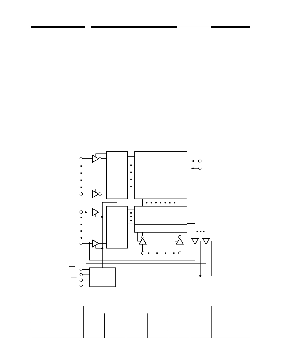
Functional Block Diagram
Row
Decoder
1024 x 1024
Memory Array
Input
Data
Circuit
Column I/O
Column Decoder
Control
Circuit
V
CC
GND
A
0
3181024-01
A
9
I/O
0
I/O
7
CE
2
OE
WE
CE
1
A
10
A
16

2
V62C3181024 Rev. 1.8 September 1998
MOSEL VITELIC
V62C3181024
Part Number Information
SRAM
FAMILY
C = CMOS PROCESS
62 = STANDARD
31 = 3.0V ≠ 3.6V
OPERATING
VOLTAGE
1024K
ORGANIZATION
PKG
SPEED
3181024-05
PWR.
62
C
8
31
1024
≠
MOSEL-VITELIC
MANUFACTURED
V
8 = 8-bit
45 ns
70 ns
TEMP.
BLANK = 0
°
C to 70
°
C
I = -40
°
C to +85
°
C
L = LOW POWER
LL = DOUBLE LOW POWER
T = TSOP STANDARD
W = 440 mil SOP (525 mil pin-to-pin)
DENSITY
Absolute Maximum Ratings
(1)
NOTE:
1.
Stresses greater than those listed under "Absolute Maximum Ratings" may cause permanent damage to the device. This is a stress
rating only and functional operation of the device at these or any other conditions above those indicated in the operational sections
of this specification is not implied. Exposure to absolute maximum rating conditions for extended periods may affect reliability.
Symbol
Parameter
Commercial
Industrial
Units
V
CC
Supply Voltage
-0.5 to V
CC
+0.5
-0.5 to V
CC
+0.5
V
V
N
Input Voltage
-0.5 to +0.5
-0.5 to +0.5
V
V
DQ
Input/Output Voltage Applied
V
CC
+ 0.3
V
CC
+ 0.3
V
T
BIAS
Temperature Under Bias
-10 to +125
-65 to +135
∞
C
T
STG
Storage Temperature
-55 to +125
-65 to +150
∞
C
Capacitance*
T
A
= 25
∞
C, f = 1.0MHz
NOTE:
1.
This parameter is guaranteed and not tested.
Truth Table
NOTE:
X = Don't Care, L = LOW, H = HIGH
Symbol
Parameter Conditions
Max.
Unit
C
IN
Input Capacitance
V
IN
= 0V
6
pF
C
OUT
Output Capacitance
V
I/O
= 0V
8
pF
Mode
CE
1
CE
2
OE
WE
I/O
Operation
Standby
H
X
X
X
High Z
Standby
X
L
X
X
High Z
Output Disable
L
H
H
H
High Z
Read
L
H
L
H
D
OUT
Write
L
H
X
L
D
IN
MOSEL VITELIC
V62C3181024
3
V62C3181024 Rev. 1.8 September 1998
DC Electrical Characteristics
(over all temperature ranges, V
CC
=3.0V≠3.6V)
NOTES:
1.
These are absolute values with respect to device ground and all overshoots due to system or tester noise are included.
2.
V
IL
(Min.) = -3.0V for pulse width < 20ns.
3.
f
MAX
= 1/t
RC
.
4.
Maximum values.
Symbol
Parameter
Test Conditions
Min.
Typ.
Max.
Units
V
CC
Power Supply Voltage
3.0
3.6
V
V
IL
Input LOW Voltage
(1,2)
-0.3
--
0.8
V
V
IH
Input HIGH Voltage
(1)
2.2
--
V
CC
+0.3
V
I
IL
Input Leakage Current
V
CC
= Max, V
IN
= 0V to V
CC
-2
--
2
m
A
I
OL
Output Leakage Current
V
CC
= Max, CE
1
= V
IH
, V
OUT
= 0V to V
CC
-2
--
2
m
A
V
OL
Output LOW Voltage
V
CC
= Min, I
OL
= 2.1mA
--
--
0.4
V
V
OH
Output HIGH Voltage
V
CC
= Min, I
OH
= -1mA
2.4
--
--
V
Symbol
Parameter
Power
Com.
(4)
Ind.
(4)
Units
I
CC
Operating Power Supply Current, CE
1
= V
IL
, CE
2
= V
IH
,
Output Open, V
CC
= Max., f = 0
READ
L
4
6
mA
LL
3
5
WRITE
L
30
35
LL
25
30
I
CC1
Average Operating Current, CE
1
= V
IL
, CE
2
= V
IH
, Output Open,
V
CC
= Max., f = f
MAX
(3)
60
80
mA
I
SB
TTL Standby Current
CE
1
≥
V
IH
, CE
2
£
V
IL
, V
CC
= Max.
L
2
4
mA
LL
1
3
I
SB1
CMOS Standby Current, CE
1
≥
V
CC
≠ 0.2V, CE
2
£
0.2V,
V
IN
≥
V
CC
≠ 0.2V or V
IN
£
0.2V, V
CC
= Max.
L
50
60
m
A
LL
30
50
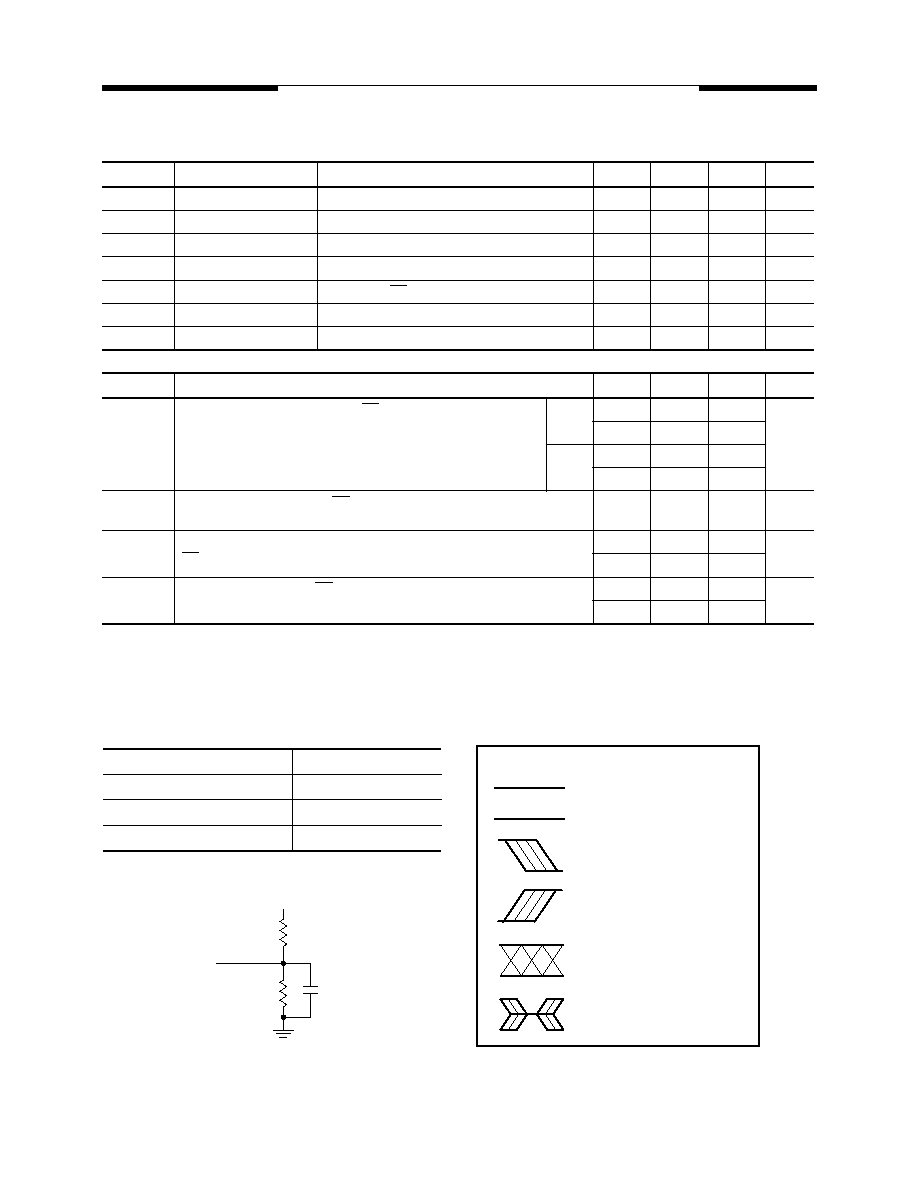
AC Test Conditions
AC Test Loads and Waveforms
Key to Switching Waveforms
Input Pulse Levels
0 to 3V
Input Rise and Fall Times
5 ns
Timing Reference Levels
1.5V
Output Load
see below
+3V
1103
Ω
1554
Ω
* Includes scope and jig capacitance
I/O Pins
C
L
= 30 pF*
3181024-06
WAVEFORM
INPUTS
OUTPUTS
MUST BE
STEADY
WILL BE
STEADY
MAY CHANGE
FROM H TO L
WILL BE
CHANGING
FROM H TO L
MAY CHANGE
FROM L TO H
WILL BE
CHANGING
FROM L TO H
DON'T CARE:
ANY CHANGE
PERMITTED
CHANGING:
STATE
UNKNOWN
DOES NOT
APPLY
CENTER
LINE IS HIGH
IMPEDANCE
"OFF" STATE
4
V62C3181024 Rev. 1.8 September 1998
MOSEL VITELIC
V62C3181024
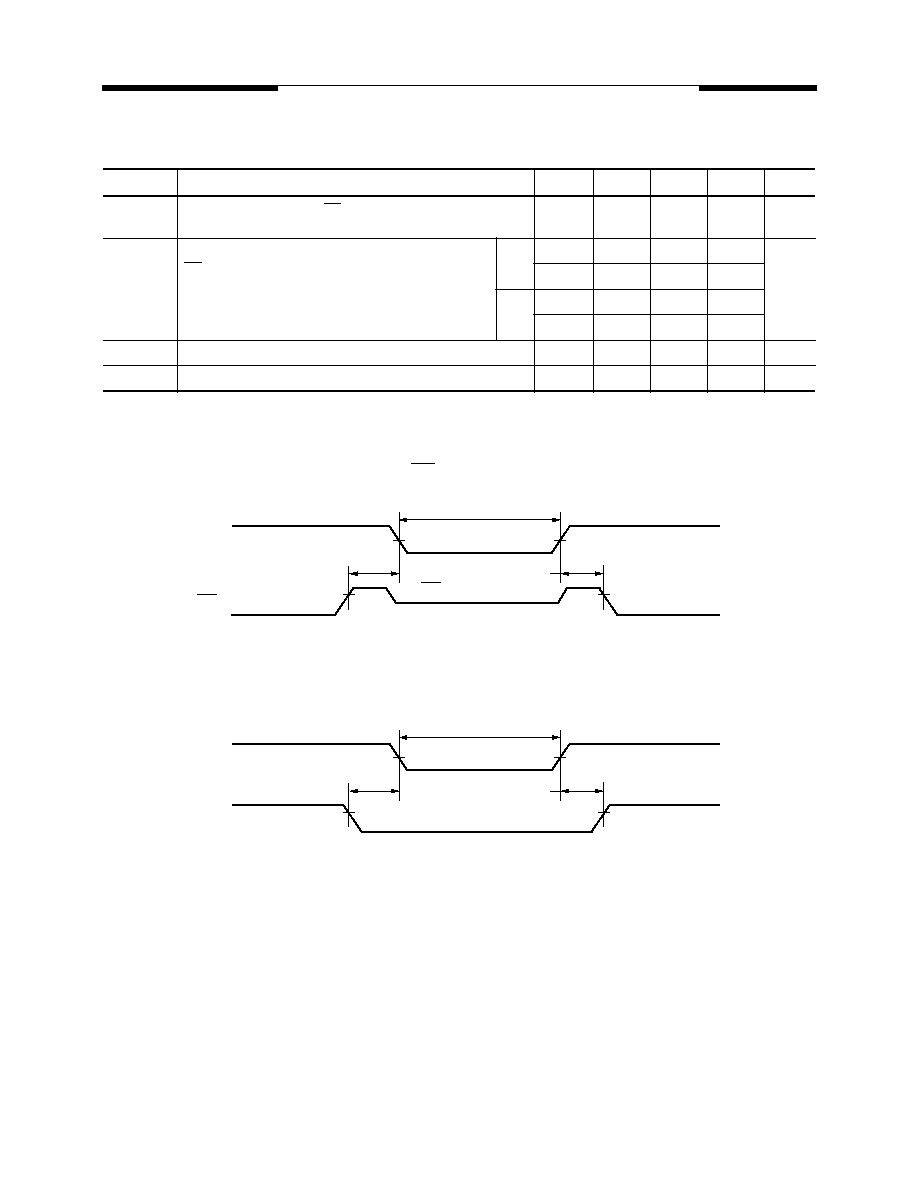
Data Retention Characteristics
NOTES:
1.
t
RC
= Read Cycle Time
2.
T
A
= +25
∞
C.
Low V
CC
Data Retention Waveform (1) (CE
1
Controlled)
Low V
CC
Data Retention Waveform (2) (CE
2
Controlled)
Symbol
Parameter
Power
Min.
Typ.
(2)
Max.
Units
V
DR
V
CC
for Data Retention
CE
1
≥
V
CC
≠ 0.2V, CE
2
£
0.2V,
V
IN
≥
V
CC
≠ 0.2V, or V
IN
£
0.2V
2.0
--
3.6
V
I
CCDR
Data Retention Current
CE
1
≥
V
DR
≠0.2V, CE
2
£
0.2V,
V
IN
≥
V
CC
≠ 0.2V, or V
IN
£
0.2V
Com'l
L
--
2
40
m
A
LL
--
1
25
Ind.
L
--
--
50
LL
--
--
40
t
CDR
Chip Deselect to Data Retention Time
0
--
--
ns
t
R
Operation Recovery Time (see Retention Waveform)
t
RC
(1)
--
--
ns
V
CC
3181024-07
Data Retention Mode
CE
1
≥
V
CC
≠ 0.2V
CE
1
2.2V
2.2V
2.7V
t
CDR
t
R
V
DR
≥
2V
2.7V
V
CC
3181024-08
Data Retention Mode
CE
2
≤
0.2V
CE
2
2.2V
2.2V
2.7V
t
CDR
t
R
V
DR
≥
2V
2.7V
MOSEL VITELIC
V62C3181024
5
V62C3181024 Rev. 1.8 September 1998
AC Electrical Characteristics
(over all temperature ranges, V
CC
= 3.0V ≠ 3.6V)
Read Cycle
Write Cycle
Parameter
Name
Parameter
-45
-70
Unit
Min.
Max.
Min.
Max.
t
RC
Read Cycle Time
45
--
70
--
ns
t
AA
Address Access Time
--
45
--
70
ns
t
ACS1
Chip Enable Access Time
--
45
--
70
ns
t
ACS2
Chip Enable Access Time
--
45
--
70
ns
t
OE
Output Enable to Output Valid
--
15
--
35
ns
t
CLZ1
Chip Enable to Output in Low Z
5
--
10
--
ns
t
CLZ2
Chip Enable to Output in Low Z
5
--
10
--
ns
t
OLZ
Output Enable to Output in Low Z
5
--
5
--
ns
t
CHZ
Chip Disable to Output in High Z
0
15
0
25
ns
t
OHZ
Output Disable to Output in High Z
0
15
0
25
ns
t
OH
Output Hold from Address Change
3
--
3
--
ns
t
PU
Chip Enable to Power Up Time
0
--
0
--
ns
t
PD
Chip Enable to Power Down Time
--
45
--
70
ns
Parameter
Name
Parameter
-45
-70
Unit
Min.
Max.
Min.
Max.
t
WC
Write Cycle Time
45
--
70
--
ns
t
CW1
Chip Enable to End of Write
35
--
60
--
ns
t
CW2
Chip Enable to End of Write
35
--
60
--
ns
t
AS
Address Setup Time
0
--
0
--
ns
t
AW
Address Valid to End of Write
35
--
60
--
ns
t
WP
Write Pulse Width
35
--
50
--
ns
t
WR
Write Recovery Time
0
--
0
--
ns
t
WHZ
Write to Output High-Z
0
15
0
25
ns
t
WLZ
Write to Output Low Z
3
--
5
--
ns
t
DW
Data Setup to End of Write
20
--
30
--
ns
t
DH
Data Hold from End of Write
0
--
0
--
ns