
MC805256K36
9-Mbit: 256Kx36
Symmetric Pipelined Burst SRAM
DS15, Rev 0.5 - 10/14/00
Preliminary Information
Page 1
© 2000 MoSys Inc., All Rights Reserved, 1020 Stewart Drive, Sunnyvale, CA 94085
M S
YS
O
Æ
∑
High Performance
133-200MHz Speed grades
3-1-1-1 Burst Read
3-1-1-1 Burst Write
3-1-1-1-1-1-1-1... pipelined operation
∑
Symmetric Pipeline
No bus turnaround latency allowing 100% bus
efficiency
∑
Low Power
Low active power
Low power ZZ standby mode
2.5V Core power supply (V
DD
)
2.5-3.3V I/O power supply (V
DDQ
)
∑
Compatibility
Individual Byte Write masking
Interleaved and burst address support
Three chip enable inputs
Clock Enable and Suspend
Industry standard 100-Pin pinout
∑
Applications
Ideal for high speed, low power data and tele-
communications applications
______________________________________________
Overview
The MoSys MC805256K36 is a high performance,
low power symmetric pipelined-burst-SRAM
(SPSRAM). Fabricated using an advanced low
power, high performance CMOS process, the Mo-
Sys MC805256K36 is backward pin and function
compatible with industry standard 64Kx36 and
128Kx36. With proper implementation, PC boards
can work transparently with 64Kx36, 128Kx36 or
256Kx36 configurations, allowing the designer
maximum configuration flexibility within a single
footprint layout.
The MoSys MC805256K36 supports SPSRAM op-
erating modes at maximum burst frequency in-
cluding indefinite pipelined read or write (3-1-1-1-1-
1-1...)
The MC805256K36 is packaged in a standard 100
lead LQFP.
Low Power
The MC805256K36 affords systems power savings
due to the benefits of its proprietary MoSys tech-
nology. Making it ideal for convection cooled appli-
cations, as well as applications requiring a large
amount of SRAM.
Part Number Designation
Example
: MC805256K36L-7R5I
Device Designation:
MC8
:, Series:
05
Organization:
256K36
Package Type: L=LQFP
Speed: ≠ 7R5 133MHz
≠ 6
166MHz
≠ 5
200MHz
Temp:
I
= Industrial Temperature
Parameter
Symbol
-7R5
-6
-5
Units
Cycle Time
tKC
7.5
6
5
ns
Access Time
tKQ
4.2
3.5
3.0
ns
Clock to High-Z
tKQHZ
3.8
3.1
2.9
ns
1
DQP3
80
DQP2
10
VSSQ
71
VSSQ
19
DQ26
62
CE
2#
DQ7
39
2
DQ17
79
DQ16
11
VDDQ
70
A6
VDDQ
31
LB
O
#
20
VDDQ
61
VD
D
VDDQ
40
VSS
3
DQ18
78
DQ15
12
DQ23
69
A7
DQ10
DQ9
32
A5
21
VSSQ
60
VSS
VSSQ
41
VD
D
4
VDDQ
77
VDDQ
13
DQ24
68
CE
1#
33
A4
22
DQ27
59
CLK
DQ6
42
5
VSSQ
76
VSSQ
14
VDD
67
CE
2
VSS
34
A3
23
DQ28
58
WE
#
DQ5
43
6
DQ19
75
DQ14
15
VDD
66
BW
4
#
VDD
35
A2
24
DQ29
57
C
KE#
DQ4
44
A1
0
28
DQ31
53
A1
7
DQ2
48
A1
4
7
DQ20
74
DQ13
16
VDD
65
BW
3
#
VDD
36
A1
25
DQ30
56
OE
#
DQ3
45
A1
1
29
DQ32
52
A8
DQ1
49
A1
5
8
DQ21
73
DQ12
17
VSS
64
BW
2
#
ZZ
37
A0
26
VSSQ
55
AD
V/
L
D
#
VSSQ
46
A1
2
30
DQP4
51
A9
DQP1
50
A1
6
9
DQ22
72
DQ11
18
DQ25
63
BW
1
#
DQ8
38
100
91
82
99
90
81
98
89
97
88
96
87
95
86
94
85
93
84
92
83
27
VDDQ
54
NC (
A
18)
VDDQ
47
A1
3
100 Pin LQFP
20 mm x 14 mm body
0.65 mm nominal pin pitch
NC
NC
NC
NC
MC805256K36
9-Mbit: 256Kx36
Symmetric Pipelined Burst SRAM
DS15, Rev 0.5 - 10/14/00
Preliminary Information
Page 2
© 2000 MoSys Inc., All Rights Reserved, 1020 Stewart Drive, Sunnyvale, CA 94085
M S
YS
O
Æ
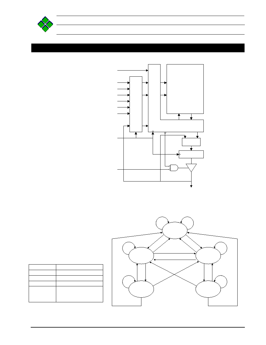
DESELECT
BEGIN
READ
BEGIN
WRITE
BURST
READ
BURST
WRITE
BURST
DS
WRITE
BURST
BURST
READ
DS
DS
WRITE
READ
READ
WRITE
BURST
BURST
READ
WRITE
WRITE
READ
DS
DS
Functional Block Diagram
Command
Action
DS
DESELECT
READ
Begin READ
WRITE
Begin WRITE
BURST
Begin READ
Begin WRITE
Continue DESELECT
State Diagram
256Kx36 Bit
Memory Array
Control Logic
Mux
Output Register
MODE
A[17:0]
CE1#, CE2, CE2#
WE#
CKE#
ADV/LD#
BW[4:1]#
CLK
OE#
DQ[32:1]
DQP[4:1]
Input Register
Address
Control
D
D
D
Q
Q
Q
Q
D

MC805256K36
9-Mbit: 256Kx36
Symmetric Pipelined Burst SRAM
DS15, Rev 0.5 - 10/14/00
Preliminary Information
Page 3
© 2000 MoSys Inc., All Rights Reserved, 1020 Stewart Drive, Sunnyvale, CA 94085
M S
YS
O
Æ
Command Truth Table
CE1#
CE2
CE2#
ZZ
ADV/
LD#
WE#
BWx#
OE#
CKE#
CLK
Address
Used
Operation
H
X
X
L
L
X
X
X
L
…
None
Deselect
X
L
X
L
L
X
X
X
L
…
None
Deselect
X
X
H
L
L
X
X
X
L
…
None
Deselect
X
X
X
L
H
X
X
X
L
…
None
Continue Deselect
L
H
L
L
L
H
X
L
L
…
External
Read Start
X
X
X
L
H
X
X
L
L
…
Next
Read Burst
L
H
L
L
L
H
X
H
L
…
External
Dummy Read
X
X
X
L
H
X
X
H
L
…
Next
Dummy Read
L
H
L
L
L
L
L
X
L
…
External
Write Start
X
X
X
L
H
X
L
X
L
…
Next
Write Burst
L
H
L
L
L
L
H
X
L
…
None
Write Abort
X
X
X
L
H
X
H
X
L
…
Next
Write Abort
X
X
X
L
X
X
X
X
H
…
Current
Ignore Clock
X
X
X
H
X
X
X
X
X
X
None
Sleep
Partial Read/Write Truth Table
WE#
BW4#
BW3#
BW2#
BW1#
Operation
H
X
X
X
X
READ
L
L
H
H
H
WRITE DQ[32:25] & DQP[4]
L
H
L
H
H
WRITE DQ[24:17] & DQP[3]
L
H
H
L
H
WRITE DQ[16:9] & DQP[2]
L
H
H
H
L
WRITE DQ[8:1] & DQP[1]
L
L
L
L
L
WRITE All DQ & DQP
L
H
H
H
H
WRITE Abort/NOP
Address Burst Sequence Tables
A[1:0]
A[1:0]
A[1:0]
A[1:0]
Linear Address, LBO#=L
00
01
10
11
1
st
Address
01
10
11
00
2
nd
Address
10
11
00
01
3
rd
Address
11
00
01
10
4
th
Address
A[1:0]
A[1:0]
A[1:0]
A[1:0]
Interleaved Address, LBO#=H
00
01
10
11
1
st
Address
01
00
11
10
2
nd
Address
10
11
00
01
3
rd
Address
11
10
01
00
4
th
Address

MC805256K36
9-Mbit: 256Kx36
Symmetric Pipelined Burst SRAM
DS15, Rev 0.5 - 10/14/00
Preliminary Information
Page 4
© 2000 MoSys Inc., All Rights Reserved, 1020 Stewart Drive, Sunnyvale, CA 94085
M S
YS
O
Æ
Pin Description
Pin Number
Symbol
Type
Description
83, 50, 49, 48, 47, 46, 45, 44, 81, 82,
99, 100, 32, 33, 34, 35, 36 ,37
A[17:0]
Input
Processor Addresses
96,95, 94, 93
BW[4:1]#
Input
Processor host bus byte enables
88
WE#
Input
Read/Write Control
87
CKE#
Input
Clock Enable
89
CLK
Input
Processor host bus clock
98
CE1#
Input
Chip enable
97
CE2
Input
Chip enable for depth expansion
92
CE2#
Input
Chip enable for depth expansion
86
OE#
Input
Asynchronous output enable
85
ADV/LD#
Input
Address Advance/Load# control
64
ZZ
Input
Low power sleep mode
31
LBO#
Input
Linear Burst Order
29, 28, 25, 24, 23, 22, 19, 18, 13, 12, 9,
8, 7, 6, 3, 2, 79, 78, 75, 74, 73, 72, 69,
68, 63, 62, 59, 58, 57, 56, 53, 52
DQ[32:1]
I/O
Data I/O pins
30, 1, 80, 51
DQP[4:1]
-
Data Parity I/O pins
38, 39, 42, 43, 84
NC
-
unused
14, 15, 16, 41, 65, 66, 91
VDD
2.5 Volts
Power
17, 40, 67, 90
VSS
Ground
Ground
4, 11, 20, 27, 54, 61, 70, 77
VDDQ
2.5 Volts
I/O Buffer Supply
5, 10, 21, 26, 55, 60, 71, 76
VSSQ
Ground
I/O Buffer Ground
Absolute Maximum Ratings
Symbol
Parameter
Min
Max
Units
VDD
Core Supply Voltage
3.6
V
VDDQ
I/O Supply Voltage
VDDQ VDD +1.0,
VDDQ 3.6
V
Vih
Input High Voltage
VDDQ +1
V
Vil
Input Low Voltage
VSSQ-0.5
V
Ts
Storage Temperature
-65
150
∞
C
Notes: Max Vih is not to exceed maximum VDDQ
Capacitance
Symbol
Parameter
Typ
Max
Units
CI
Input Capacitance
3
4
V
CIO
I/O Capacitance
4
5
V
LQFP Thermal Resistance
Symbol
Parameter
Typ
Units
JA
Junction to Ambient
45
∞
C/W
JC
Junction to Case
9
∞
C/W
MC805256K36
9-Mbit: 256Kx36
Symmetric Pipelined Burst SRAM
DS15, Rev 0.5 - 10/14/00
Preliminary Information
Page 5
© 2000 MoSys Inc., All Rights Reserved, 1020 Stewart Drive, Sunnyvale, CA 94085
M S
YS
O
Æ
Recommended Operating Conditions
Symbol
Parameter
Condition
Min
Max
Units
VDD
Supply Voltage
2.5V ± 5%
2.375
2.625
V
VDDQ
I/O Supply Voltage
2.5V ± 5%
2.375
2.625
V
Vih
Input High Voltage
1.7
V
DDQ
+ .8
V
Vil
Input Low Voltage
-0.3
0.7
V
Voh
Output High Voltage
Ioh = -1 mA
2.0
V
Vol
Output Low Voltage
Iol = 1 mA
0.2
V
Toprc
Commercial Operating Temp.
0
70
∞
C
Topri
Industrial Operating Temp.
-40
85
∞
C
Absolute Maximum AC Operating Conditions
Symbol
Parameter
Min
Max
Units
Vih
Input High Voltage
1.7
V
DDQ
+1.0
V
Vil
Input Low Voltage
V
SSQ
- 1.0
0.7
V
tOVR
Overshoot/Undershoot Voltage Duration
0.2*tCY
ns
tSET
Overshoot/Undershoot Settling Time
0.8*tCY
ns
Maximum DC Current Requirements
Symbol
Condition
Current
Units
I
DD
Operating current, device selected; all inputs < Vil or > Vih; cycle time > 7.5ns,
VDD= max, 0 pF load
150
mA
I
DD1
Idle current; ADV/LD#, GW#, BW#s, CKE# and all other inputs > 2.8 volts; cycle
time > tKC min, VDD= max, 0 pF load
40
mA
I
DDZ
Sleep mode, clock stopped, all inputs > 2.8 v, VDD= max
20
mA