 | –≠–ª–µ–∫—Ç—Ä–æ–Ω–Ω—ã–π –∫–æ–º–ø–æ–Ω–µ–Ω—Ç: 2N2369 | –°–∫–∞—á–∞—Ç—å:  PDF PDF  ZIP ZIP |

1
Motorola Small≠Signal Transistors, FETs and Diodes Device Data
Switching Transistors
NPN Silicon
MAXIMUM RATINGS
Rating
Symbol
Value
Unit
Collector ≠ Emitter Voltage
VCEO
15
Vdc
Collector ≠ Emitter Voltage
VCES
40
Vdc
Collector≠ Base Voltage
VCBO
40
Vdc
Emitter≠ Base Voltage
VEBO
4.5
Vdc
Collector Current (10
m
s pulse)
IC(Peak)
500
mA
Collector Current -- Continuous
IC
200
mA
Total Device Dissipation @ TA = 25
∞
C
Derate above 25
∞
C
PD
0.36
2.06
Watt
mW/
∞
C
Total Device Dissipation @ TC = 100
∞
C
Derate above 100
∞
C
PD
0.68
6.85
Watts
mW/
∞
C
Operating and Storage Junction
Temperature Range
TJ, Tstg
≠ 65 to +200
∞
C
THERMAL CHARACTERISTICS
Characteristic
Symbol
Max
Unit
Thermal Resistance, Junction to Ambient
R
q
JA
486
∞
C/W
Thermal Resistance, Junction to Case
R
q
JC
147
∞
C/W
ELECTRICAL CHARACTERISTICS
(TA = 25
∞
C unless otherwise noted)
Characteristic
Symbol
Min
Max
Unit
OFF CHARACTERISTICS
Collector ≠ Emitter Breakdown Voltage (IC = 10
m
A, VBE = 0)
V(BR)CES
40
--
Vdc
Collector ≠ Emitter Sustaining Voltage(1) (IC = 10 mAdc, IB = 0)
VCEO(sus)
15
--
Vdc
Collector ≠ Base Breakdown Voltage (IC = 10
m
A, IB = 0)
V(BR)CBO
40
--
Vdc
Emitter ≠ Base Breakdown Voltage (IE = 10
m
Adc, IC = 0)
V(BR)EBO
4.5
--
Vdc
Collector Cutoff Current
(VCB = 20 Vdc, IE = 0)
2N2369
(VCB = 20 Vdc, IE = 0, TA = 150
∞
C)
2N2369A
ICBO
--
--
0.4
30
m
Adc
Collector Cutoff Current
(VCE = 20 Vdc, VBE = 0)
2N2369A
ICES
--
0.4
m
Adc
Base Current
(VCE = 20 Vdc, VBE = 0)
2N2369A
IB
--
0.4
m
Adc
1. Pulse Test: Pulse Width
v
300
m
s, Duty Cycle
v
2.0%.
Preferred devices are Motorola recommended choices for future use and best overall value.
Order this document
by 2N2369/D
MOTOROLA
SEMICONDUCTOR TECHNICAL DATA
2N2369
2N2369A
*Motorola Preferred Device
CASE 22≠03, STYLE 1
TO≠18 (TO≠206AA)
1
2
3
*
©
Motorola, Inc. 1996
COLLECTOR
3
2
BASE
1
EMITTER

2N2369 2N2369A
2
Motorola Small≠Signal Transistors, FETs and Diodes Device Data
ELECTRICAL CHARACTERISTICS
(TA = 25
∞
C unless otherwise noted) (Continued)
Characteristic
Symbol
Min
Max
Unit
ON CHARACTERISTICS
DC Current Gain(1)
(IC = 10 mAdc, VCE = 1.0 Vdc)
2N2369
2N2369A
(IC = 10 mAdc, VCE = 1.0 Vdc, TA = ≠55
∞
C)
2N2369
(IC = 10 mAdc, VCE = 0.35 Vdc, TA = ≠55
∞
C)
2N2369A
(IC = 30 mAdc, VCE = 0.4 Vdc)
2N2369A
(IC = 100 mAdc, VCE = 1.0 Vdc)
2N2369A
(IC = 100 mAdc, VCE = 2.0 Vdc)
2N2369
hFE
40
--
20
20
30
20
20
120
120
--
--
--
--
--
--
Collector ≠ Emitter Saturation Voltage(1)
(IC = 10 mAdc, IB = 1.0 mAdc)
2N2369
2N2369A
(IC = 10 mAdc, IB = 1.0 mAdc, TA = +125
∞
C)
2N2369A
(IC = 30 mAdc, IB = 3.0 mAdc)
2N2369A
(IC = 100 mAdc, IB = 10 mAdc)
2N2369A
VCE(sat)
--
--
--
--
--
0.25
0.20
0.30
0.25
0.50
Vdc
Base ≠ Emitter Saturation Voltage(1)
(IC = 10 mAdc, IB = 1.0 mAdc)
All Types
(IC = 10 mAdc, IB = 1.0 mAdc, TA = +125
∞
C)
2N2369A
(IC = 10 mAdc, IB = 1.0 mAdc, TA = ≠55
∞
C)
2N2369A
(IC = 30 mAdc, IB = 3.0 mAdc)
2N2369A
(IC = 100 mAdc, IB = 10 mAdc)
2N2369A
VBE(sat)
0.70
0.59
--
--
--
0.85
--
1.02
1.15
1.60
Vdc
SMALL≠ SIGNAL CHARACTERISTICS
Current ≠ Gain -- Bandwidth Product
(IC = 10 mAdc, VCE = 10 Vdc, f = 100 MHz)
fT
500
--
MHz
Output Capacitance
(VCB = 5.0 Vdc, IE = 0, f = 1.0 MHz)
Cobo
--
4.0
pF
Input Capacitance
(VEB = 1.0 Vdc, IC = 0, f = 1.0 MHz)
Cibo
--
4.0
pF
SWITCHING CHARACTERISTICS
Storage Time
(IC = IB1 = 10 mAdc, IB2 = ≠10 mAdc)
ts
--
13
ns
Turn≠On Time
(IC = 10 mAdc, IB1 = 3.0 mA, IB2 = ≠1.5 mA, VCC = 3.0 Vdc)
ton
--
12
ns
Turn≠Off Time
(IC = 10 mAdc, IB1 = 3.0 mA, IB2 = ≠1.5 mA, VCC = 3.0 Vdc)
toff
--
18
ns
1. Pulse Test: Pulse Width
v
300
m
s, Duty Cycle
v
2.0%.
2N2369 2N2369A
3
Motorola Small≠Signal Transistors, FETs and Diodes Device Data
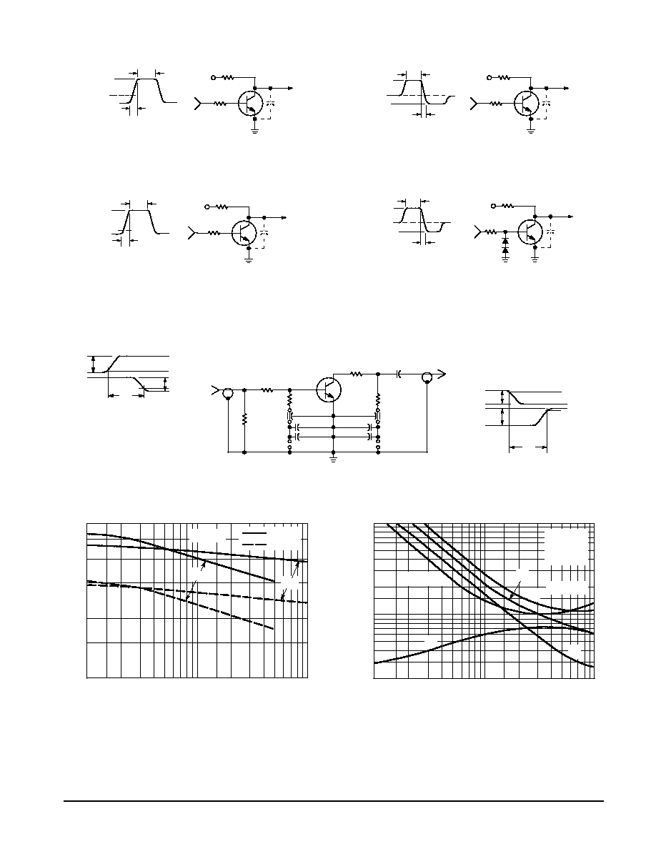
Figure 1. ton Circuit -- 10 mA
Figure 2. ton Circuit -- 100 mA
Figure 3. toff Circuit -- 10 mA
Figure 4. toff Circuit -- 100 mA
Figure 5. Turn≠On and Turn≠Off Time Test Circuit
+10.6 V
≠1.5 V
0
t1
< 1 ns
PULSE WIDTH (t1) = 300 ns
DUTY CYCLE = 2%
3 V
270
3.3 k
Cs* < 4 pF
10 V
95
1 k
Cs* < 12 pF
+10.8 V
≠2 V
0
t1
< 1 ns
PULSE WIDTH (t1) = 300 ns
DUTY CYCLE = 2%
+10.75 V
0
≠9.15 V
t1
< 1 ns
PULSE WIDTH (t1) = 300 ns
DUTY CYCLE = 2%
< 1 ns
≠8.6 V
+11.4 V
t1
0
PULSE WIDTH (t1) BETWEEN
10 AND 500
µ
s
DUTY CYCLE = 2%
270
3.3 k
Cs* < 4 pF
95
1 k
Cs* < 12 pF
10 V
1N916
SWITCHING TIME EQUIVALENT TEST CIRCUITS FOR 2N2369, 2N3227
Vout
90%
10%
Vin
0
ton
Vin
3.3 k
50
220
50
0.1
µ
F
Vout
3.3 k
0.0023
µ
F
0.0023
µ
F
0.005
µ
F
0.005
µ
F
0.1
µ
F
0.1
µ
F
VBB +≠
+
≠ VCC = 3 V
Vin
0
90%
10%
toff
Vout
VBB = +12 V
Vin = ≠15 V
TO OSCILLOSCOPE
INPUT IMPEDANCE = 50
RISE TIME = 1 ns
TURN≠OFF WAVEFORMS
PULSE GENERATOR
Vin RISE TIME < 1 ns
SOURCE IMPEDANCE = 50
PW
300 ns
DUTY CYCLE < 2%
TURN≠ON WAVEFORMS
* Total shunt capacitance of test jig and connectors.
6
5
4
3
2
1
10
0.1
0.2
0.5
1.0
2.0
5.0
REVERSE BIAS (VOLTS)
CAP
ACIT
ANCE (pF)
SWITCHING
TIMES (nsec)
LIMIT
TYPICAL
Cob
Cib
TJ = 25
∞
C
Figure 6. Junction Capacitance Variations
100
2
5
10
20
50
1
2
5
10
20
50
100
IC, COLLECTOR CURRENT (mA)
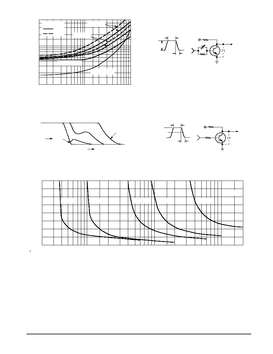
Figure 7. Typical Switching Times
F = 10
VCC = 10 V
VOB = 2 V
tr (VCC = 3 V)
VCC = 10 V
td
ts
tr
tf
2N2369 2N2369A
4
Motorola Small≠Signal Transistors, FETs and Diodes Device Data
25
∞
C
100
∞
C
QT,
F = 10
500
1
IC, COLLECTOR CURRENT (mA)
Figure 8. Maximum Charge Data
10
20
50
100
200
2
5
10
20
50
100
VCC = 10 V
QT,
F = 40
QA, VCC = 10 V
QA, VCC = 3 V
CHARGE (pC)
+5 V
0
t1
< 1 ns
PULSE WIDTH (t1) = 5
µ
s
DUTY CYCLE = 2%
3 V
270
4.3 k
Cs* < 4 pF
V
10 pF MAX
VALUES REFER TO
IC = 10 mA TEST
Figure 9. QT Test Circuit
+6 V
≠4 V
0
t1
< 1 ns
PULSE WIDTH (t1) = 300 ns
DUTY CYCLE = 2%
10 V
980
500
Cs* < 3 pF
C
COPT
TIME
C < COPT
C = 0
Figure 10. Turn≠Off Waveform
Figure 11. Storage Time Equivalent Test Circuit
V
CE
, MAXIMUM COLLECT
OR≠EMITTER VOL
T
AGE (VOL
TS)
1.0
0.8
0.6
0.4
0.2
0.02
0.05
0.1
0.2
0.5
1
2
5
10
20
IC = 3 mA
IC = 10 mA
IC = 30 mA
IC = 50 mA
IC = 100 mA
TJ = 25
∞
C
IB, BASE CURRENT (mA)
Figure 12. Maximum Collector Saturation Voltage Characteristics

2N2369 2N2369A
5
Motorola Small≠Signal Transistors, FETs and Diodes Device Data
h
FE
, MINIMUM DC CURRENT
GAIN
V
(sat)
, SA
TURA
TION VOL
T
AGE (VOL
TS)
COEFFICIENT
(mV/
C)
∞
200
100
20
50
1
2
5
10
20
50
100
IC, COLLECTOR CURRENT (mA)
Figure 13. Minimum Current Gain Characteristics
VCE = 1 V
TJ = 125
∞
C
75
∞
C
25
∞
C
≠15
∞
C
≠55
∞
C
TJ = 25
∞
C and 75
∞
C
1.4
1.2
1.0
0.8
0.6
0.4
0.2
1
2
5
10
20
50
100
IC, COLLECTOR CURRENT (mA)
Figure 14. Saturation Voltage Limits
1.0
0.5
0
≠0.5
≠1.0
≠1.5
≠2.0
≠2.5
0
10
20
30
40
50
60
70
80
90
100
IC, COLLECTOR CURRENT (mA)
Figure 15. Typical Temperature Coefficients
F = 10
TJ = 25
∞
C
MAX VBE(sat)
MIN VBE(sat)
MAX VCE(sat)
(25
∞
C to 125
∞
C)
(≠55
∞
C to +25
∞
C)
(≠55
∞
C to +25
∞
C)
(25
∞
C to 125
∞
C)
VC for VCE(sat)
VB for VBE(sat)
≠55
∞
C to +25
∞
C
25
∞
C to 125
∞
C
VC
±
0.15 mV/
∞
C
±
0.15 mV/
∞
C
VB
±
0.4 mV/
∞
C
±
0.3 mV/
∞
C
APPROXIMATE DEVIATION
FROM NOMINAL

2N2369 2N2369A
6
Motorola Small≠Signal Transistors, FETs and Diodes Device Data
PACKAGE DIMENSIONS
CASE 22≠03
(TO≠206AA)
ISSUE R
SEATING
PLANE
E
F
B
C
K
L
P
D
3 PL
≠T≠
≠H≠
M
J
G
2
3
1
M
A
M
0.36 (0.014)
H
M
T
N
N
≠A≠
DIM
MIN
MAX
MIN
MAX
MILLIMETERS
INCHES
A
0.209
0.230
5.31
5.84
B
0.178
0.195
4.52
4.95
C
0.170
0.210
4.32
5.33
D
0.016
0.021
0.406
0.533
E
≠≠≠
0.030
≠≠≠
0.762
F
0.016
0.019
0.406
0.483
G
0.100 BSC
2.54 BSC
H
0.036
0.046
0.914
1.17
J
0.028
0.048
0.711
1.22
K
0.500
≠≠≠
12.70
≠≠≠
L
0.250
≠≠≠
6.35
≠≠≠
M
45 BSC
45 BSC
N
0.050 BSC
1.27 BSC
P
≠≠≠
0.050
≠≠≠
1.27
_
_
NOTES:
1. DIMENSIONING AND TOLERANCING PER ANSI
Y14.5M, 1982.
2. CONTROLLING DIMENSION: INCH.
3. DIMENSION J MEASURED FROM DIMENSION A
MAXIMUM.
4. DIMENSION F APPLIES BETWEEN DIMENSION P
AND L. DIMENSION D APPLIES BETWEEN
DIMENSION L AND K MINIMUM. LEAD DIAMETER
IS UNCONTROLLED IN DIMENSION P AND
BEYOND DIMENSION K MINIMUM.
5. DIMENSION E INCLUDES THE TAB THICKNESS.
(TAB THICKNESS IS 0.51(0.002) MAXIMUM).
STYLE 1:
PIN 1. EMITTER
2. BASE
3. COLLECTOR
Motorola reserves the right to make changes without further notice to any products herein. Motorola makes no warranty, representation or guarantee regarding
the suitability of its products for any particular purpose, nor does Motorola assume any liability arising out of the application or use of any product or circuit, and
specifically disclaims any and all liability, including without limitation consequential or incidental damages. "Typical" parameters which may be provided in Motorola
data sheets and/or specifications can and do vary in different applications and actual performance may vary over time. All operating parameters, including "Typicals"
must be validated for each customer application by customer's technical experts. Motorola does not convey any license under its patent rights nor the rights of
others. Motorola products are not designed, intended, or authorized for use as components in systems intended for surgical implant into the body, or other
applications intended to support or sustain life, or for any other application in which the failure of the Motorola product could create a situation where personal injury
or death may occur. Should Buyer purchase or use Motorola products for any such unintended or unauthorized application, Buyer shall indemnify and hold Motorola
and its officers, employees, subsidiaries, affiliates, and distributors harmless against all claims, costs, damages, and expenses, and reasonable attorney fees
arising out of, directly or indirectly, any claim of personal injury or death associated with such unintended or unauthorized use, even if such claim alleges that
Motorola was negligent regarding the design or manufacture of the part. Motorola and are registered trademarks of Motorola, Inc. Motorola, Inc. is an Equal
Opportunity/Affirmative Action Employer.
How to reach us:
USA / EUROPE / Locations Not Listed: Motorola Literature Distribution;
JAPAN: Nippon Motorola Ltd.; Tatsumi≠SPD≠JLDC, 6F Seibu≠Butsuryu≠Center,
P.O. Box 20912; Phoenix, Arizona 85036. 1≠800≠441≠2447 or 602≠303≠5454
3≠14≠2 Tatsumi Koto≠Ku, Tokyo 135, Japan. 03≠81≠3521≠8315
MFAX: RMFAX0@email.sps.mot.com ≠ TOUCHTONE 602≠244≠6609
ASIA/PACIFIC: Motorola Semiconductors H.K. Ltd.; 8B Tai Ping Industrial Park,
INTERNET: http://Design≠NET.com
51 Ting Kok Road, Tai Po, N.T., Hong Kong. 852≠26629298
2N2369/D
*2N2369/D*