 | –≠–ª–µ–∫—Ç—Ä–æ–Ω–Ω—ã–π –∫–æ–º–ø–æ–Ω–µ–Ω—Ç: 4066 | –°–∫–∞—á–∞—Ç—å:  PDF PDF  ZIP ZIP |

MOTOROLA
SEMICONDUCTOR TECHNICAL DATA
1
REV 6
©
Motorola, Inc. 1995
10/95
Quad Analog Switch/
Multiplexer/Demultiplexer
High≠Performance Silicon≠Gate CMOS
The MC54/74HC4066 utilizes silicon≠gate CMOS technology to achieve
fast propagation delays, low ON resistances, and low OFF≠channel leakage
current. This bilateral switch/multiplexer/demultiplexer controls analog and
digital voltages that may vary across the full power≠supply range (from VCC
to GND).
The HC4066 is identical in pinout to the metal≠gate CMOS MC14016 and
MC14066. Each device has four independent switches. The device has
been designed so that the ON resistances (RON) are much more linear over
input voltage than RON of metal≠gate CMOS analog switches.
This device is identical in both function and pinout to the HC4016. The
ON/OFF control inputs are compatible with standard CMOS outputs; with
pullup resistors, they are compatible with LSTTL outputs. For analog
switches with voltage≠level translators, see the HC4316.
∑
Fast Switching and Propagation Speeds
∑
High ON/OFF Output Voltage Ratio
∑
Low Crosstalk Between Switches
∑
Diode Protection on All Inputs/Outputs
∑
Wide Power≠Supply Voltage Range (VCC ≠ GND) = 2.0 to 12.0 Volts
∑
Analog Input Voltage Range (VCC ≠ GND) = 2.0 to 12.0 Volts
∑
Improved Linearity and Lower ON Resistance over Input Voltage than
the MC14016 or MC14066 or HC4016
∑
Low Noise
∑
Chip Complexity: 44 FETs or 11 Equivalent Gates
LOGIC DIAGRAM
XA
YA
1
2
A ON/OFF CONTROL
13
XB
YB
4
3
B ON/OFF CONTROL
5
XC
YC
8
9
C ON/OFF CONTROL
6
XD
YD
11
10
D ON/OFF CONTROL
12
ANALOG
OUTPUTS/INPUTS
ANALOG INPUTS/OUTPUTS = XA, XB, XC, XD
PIN 14 = VCC
PIN 7 = GND
MC54/74HC4066
FUNCTION TABLE
PIN ASSIGNMENT
11
12
13
14
8
9
10
5
4
3
2
1
7
6
YD
XD
D ON/OFF
CONTROL
A ON/OFF
CONTROL
VCC
XC
YC
XB
YB
YA
XA
GND
C ON/OFF
CONTROL
B ON/OFF
CONTROL
On/Off Control
State of
Input
Analog Switch
L
Off
H
On
D SUFFIX
SOIC PACKAGE
CASE 751A≠03
N SUFFIX
PLASTIC PACKAGE
CASE 646≠06
ORDERING INFORMATION
MC54HCXXXXJ
MC74HCXXXXN
MC74HCXXXXD
MC74HCXXXXDT
Ceramic
Plastic
SOIC
TSSOP
1
14
1
14
1
14
DT SUFFIX
TSSOP PACKAGE
CASE 948G≠01
J SUFFIX
CERAMIC PACKAGE
CASE 632≠08
1
14
MC54/74HC4066
MOTOROLA
High≠Speed CMOS Logic Data
DL129 -- Rev 6
2
ŒŒŒŒŒŒŒŒŒŒŒŒŒŒŒŒŒŒŒŒŒŒŒ
ŒŒŒŒŒŒŒŒŒŒŒŒŒŒŒŒŒŒŒŒŒŒŒ
ŒŒŒŒŒŒŒŒŒŒŒŒŒŒŒŒŒŒŒŒŒŒŒ
ŒŒŒŒŒŒŒŒŒŒŒŒŒŒŒŒŒŒŒŒŒŒŒ
MAXIMUM RATINGS*
ŒŒŒ
ŒŒŒ
ŒŒŒ
ŒŒŒ
Symbol
ŒŒŒŒŒŒŒŒŒŒŒŒŒŒ
ŒŒŒŒŒŒŒŒŒŒŒŒŒŒ
ŒŒŒŒŒŒŒŒŒŒŒŒŒŒ
ŒŒŒŒŒŒŒŒŒŒŒŒŒŒ
Parameter
ŒŒŒŒŒŒ
ŒŒŒŒŒŒ
ŒŒŒŒŒŒ
ŒŒŒŒŒŒ
Value
ŒŒŒ
ŒŒŒ
ŒŒŒ
ŒŒŒ
Unit
ŒŒŒ
ŒŒŒ
ŒŒŒ
ŒŒŒ
VCC
ŒŒŒŒŒŒŒŒŒŒŒŒŒŒ
ŒŒŒŒŒŒŒŒŒŒŒŒŒŒ
ŒŒŒŒŒŒŒŒŒŒŒŒŒŒ
ŒŒŒŒŒŒŒŒŒŒŒŒŒŒ
Positive DC Supply Voltage (Referenced to GND)
ŒŒŒŒŒŒ
ŒŒŒŒŒŒ
ŒŒŒŒŒŒ
ŒŒŒŒŒŒ
≠ 0.5 to + 14.0
ŒŒŒ
ŒŒŒ
ŒŒŒ
ŒŒŒ
V
ŒŒŒ
ŒŒŒ
ŒŒŒ
ŒŒŒ
VIS
ŒŒŒŒŒŒŒŒŒŒŒŒŒŒ
ŒŒŒŒŒŒŒŒŒŒŒŒŒŒ
ŒŒŒŒŒŒŒŒŒŒŒŒŒŒ
ŒŒŒŒŒŒŒŒŒŒŒŒŒŒ
Analog Input Voltage (Referenced to GND)
ŒŒŒŒŒŒ
ŒŒŒŒŒŒ
ŒŒŒŒŒŒ
ŒŒŒŒŒŒ
≠ 0.5 to VCC + 0.5
ŒŒŒ
ŒŒŒ
ŒŒŒ
ŒŒŒ
V
ŒŒŒ
ŒŒŒ
ŒŒŒ
ŒŒŒ
Vin
ŒŒŒŒŒŒŒŒŒŒŒŒŒŒ
ŒŒŒŒŒŒŒŒŒŒŒŒŒŒ
ŒŒŒŒŒŒŒŒŒŒŒŒŒŒ
ŒŒŒŒŒŒŒŒŒŒŒŒŒŒ
Digital Input Voltage (Referenced to GND)
ŒŒŒŒŒŒ
ŒŒŒŒŒŒ
ŒŒŒŒŒŒ
ŒŒŒŒŒŒ
≠ 1.5 to VCC + 1.5
ŒŒŒ
ŒŒŒ
ŒŒŒ
ŒŒŒ
V
ŒŒŒ
ŒŒŒ
ŒŒŒ
ŒŒŒ
I
ŒŒŒŒŒŒŒŒŒŒŒŒŒŒ
ŒŒŒŒŒŒŒŒŒŒŒŒŒŒ
ŒŒŒŒŒŒŒŒŒŒŒŒŒŒ
ŒŒŒŒŒŒŒŒŒŒŒŒŒŒ
DC Current Into or Out of Any Pin
ŒŒŒŒŒŒ
ŒŒŒŒŒŒ
ŒŒŒŒŒŒ
ŒŒŒŒŒŒ
±
25
ŒŒŒ
ŒŒŒ
ŒŒŒ
ŒŒŒ
mA
ŒŒŒ
ŒŒŒ
ŒŒŒ
ŒŒŒ
ŒŒŒ
PD
ŒŒŒŒŒŒŒŒŒŒŒŒŒŒ
ŒŒŒŒŒŒŒŒŒŒŒŒŒŒ
ŒŒŒŒŒŒŒŒŒŒŒŒŒŒ
ŒŒŒŒŒŒŒŒŒŒŒŒŒŒ
ŒŒŒŒŒŒŒŒŒŒŒŒŒŒ
Power Dissipation in Still Air, Plastic or Ceramic DIP
SOIC Package
TSSOP Package
ŒŒŒŒŒŒ
ŒŒŒŒŒŒ
ŒŒŒŒŒŒ
ŒŒŒŒŒŒ
ŒŒŒŒŒŒ
750
500
450
ŒŒŒ
ŒŒŒ
ŒŒŒ
ŒŒŒ
ŒŒŒ
mW
ŒŒŒ
ŒŒŒ
ŒŒŒ
ŒŒŒ
Tstg
ŒŒŒŒŒŒŒŒŒŒŒŒŒŒ
ŒŒŒŒŒŒŒŒŒŒŒŒŒŒ
ŒŒŒŒŒŒŒŒŒŒŒŒŒŒ
ŒŒŒŒŒŒŒŒŒŒŒŒŒŒ
Storage Temperature
ŒŒŒŒŒŒ
ŒŒŒŒŒŒ
ŒŒŒŒŒŒ
ŒŒŒŒŒŒ
≠ 65 to + 150
ŒŒŒ
ŒŒŒ
ŒŒŒ
ŒŒŒ
_
C
ŒŒŒ
ŒŒŒ
ŒŒŒ
ŒŒŒ
ŒŒŒ
ŒŒŒ
TL
ŒŒŒŒŒŒŒŒŒŒŒŒŒŒ
ŒŒŒŒŒŒŒŒŒŒŒŒŒŒ
ŒŒŒŒŒŒŒŒŒŒŒŒŒŒ
ŒŒŒŒŒŒŒŒŒŒŒŒŒŒ
ŒŒŒŒŒŒŒŒŒŒŒŒŒŒ
ŒŒŒŒŒŒŒŒŒŒŒŒŒŒ
Lead Temperature, 1 mm from Case for 10 Seconds
(Plastic DIP, SOIC or TSSOP Package)
(Ceramic DIP)
ŒŒŒŒŒŒ
ŒŒŒŒŒŒ
ŒŒŒŒŒŒ
ŒŒŒŒŒŒ
ŒŒŒŒŒŒ
ŒŒŒŒŒŒ
260
300
ŒŒŒ
ŒŒŒ
ŒŒŒ
ŒŒŒ
ŒŒŒ
ŒŒŒ
_
C
* Maximum Ratings are those values beyond which damage to the device may occur.
Functional operation should be restricted to the Recommended Operating Conditions.
Derating -- Plastic DIP: ≠ 10 mW/
_
C from 65
_
to 125
_
C
Ceramic DIP: ≠ 10 mW/
_
C from 100
_
to 125
_
C
SOIC Package: ≠ 7 mW/
_
C from 65
_
to 125
_
C
TSSOP Package: ≠ 6.1 mW/
_
C from 65
_
to 125
_
C
For high frequency or heavy load considerations, see Chapter 2 of the Motorola High≠Speed CMOS Data Book (DL129/D).
RECOMMENDED OPERATING CONDITIONS
ŒŒŒŒ
ŒŒŒŒ
ŒŒŒŒ
ŒŒŒŒ
Symbol
ŒŒŒŒŒŒŒŒŒŒŒŒŒŒ
ŒŒŒŒŒŒŒŒŒŒŒŒŒŒ
ŒŒŒŒŒŒŒŒŒŒŒŒŒŒ
ŒŒŒŒŒŒŒŒŒŒŒŒŒŒ
Parameter
ŒŒŒ
ŒŒŒ
ŒŒŒ
ŒŒŒ
Min
ŒŒŒ
ŒŒŒ
ŒŒŒ
ŒŒŒ
Max
ŒŒŒ
ŒŒŒ
ŒŒŒ
ŒŒŒ
Unit
ŒŒŒŒ
ŒŒŒŒ
ŒŒŒŒ
ŒŒŒŒ
VCC
ŒŒŒŒŒŒŒŒŒŒŒŒŒŒ
ŒŒŒŒŒŒŒŒŒŒŒŒŒŒ
ŒŒŒŒŒŒŒŒŒŒŒŒŒŒ
ŒŒŒŒŒŒŒŒŒŒŒŒŒŒ
Positive DC Supply Voltage (Referenced to GND)
ŒŒŒ
ŒŒŒ
ŒŒŒ
ŒŒŒ
2.0
ŒŒŒ
ŒŒŒ
ŒŒŒ
ŒŒŒ
12.0
ŒŒŒ
ŒŒŒ
ŒŒŒ
ŒŒŒ
V
ŒŒŒŒ
ŒŒŒŒ
ŒŒŒŒ
ŒŒŒŒ
VIS
ŒŒŒŒŒŒŒŒŒŒŒŒŒŒ
ŒŒŒŒŒŒŒŒŒŒŒŒŒŒ
ŒŒŒŒŒŒŒŒŒŒŒŒŒŒ
ŒŒŒŒŒŒŒŒŒŒŒŒŒŒ
Analog Input Voltage (Referenced to GND)
ŒŒŒ
ŒŒŒ
ŒŒŒ
ŒŒŒ
GND
ŒŒŒ
ŒŒŒ
ŒŒŒ
ŒŒŒ
VCC
ŒŒŒ
ŒŒŒ
ŒŒŒ
ŒŒŒ
V
ŒŒŒŒ
ŒŒŒŒ
ŒŒŒŒ
ŒŒŒŒ
Vin
ŒŒŒŒŒŒŒŒŒŒŒŒŒŒ
ŒŒŒŒŒŒŒŒŒŒŒŒŒŒ
ŒŒŒŒŒŒŒŒŒŒŒŒŒŒ
ŒŒŒŒŒŒŒŒŒŒŒŒŒŒ
Digital Input Voltage (Referenced to GND)
ŒŒŒ
ŒŒŒ
ŒŒŒ
ŒŒŒ
GND
ŒŒŒ
ŒŒŒ
ŒŒŒ
ŒŒŒ
VCC
ŒŒŒ
ŒŒŒ
ŒŒŒ
ŒŒŒ
V
ŒŒŒŒ
ŒŒŒŒ
ŒŒŒŒ
ŒŒŒŒ
VIO*
ŒŒŒŒŒŒŒŒŒŒŒŒŒŒ
ŒŒŒŒŒŒŒŒŒŒŒŒŒŒ
ŒŒŒŒŒŒŒŒŒŒŒŒŒŒ
ŒŒŒŒŒŒŒŒŒŒŒŒŒŒ
Static or Dynamic Voltage Across Switch
ŒŒŒ
ŒŒŒ
ŒŒŒ
ŒŒŒ
--
ŒŒŒ
ŒŒŒ
ŒŒŒ
ŒŒŒ
1.2
ŒŒŒ
ŒŒŒ
ŒŒŒ
ŒŒŒ
V
ŒŒŒŒ
ŒŒŒŒ
ŒŒŒŒ
ŒŒŒŒ
TA
ŒŒŒŒŒŒŒŒŒŒŒŒŒŒ
ŒŒŒŒŒŒŒŒŒŒŒŒŒŒ
ŒŒŒŒŒŒŒŒŒŒŒŒŒŒ
ŒŒŒŒŒŒŒŒŒŒŒŒŒŒ
Operating Temperature, All Package Types
ŒŒŒ
ŒŒŒ
ŒŒŒ
ŒŒŒ
≠ 55
ŒŒŒ
ŒŒŒ
ŒŒŒ
ŒŒŒ
+ 125
ŒŒŒ
ŒŒŒ
ŒŒŒ
ŒŒŒ
_
C
ŒŒŒŒ
ŒŒŒŒ
ŒŒŒŒ
ŒŒŒŒ
ŒŒŒŒ
ŒŒŒŒ
ŒŒŒŒ
tr, tf
ŒŒŒŒŒŒŒŒŒŒŒŒŒŒ
ŒŒŒŒŒŒŒŒŒŒŒŒŒŒ
ŒŒŒŒŒŒŒŒŒŒŒŒŒŒ
ŒŒŒŒŒŒŒŒŒŒŒŒŒŒ
ŒŒŒŒŒŒŒŒŒŒŒŒŒŒ
ŒŒŒŒŒŒŒŒŒŒŒŒŒŒ
ŒŒŒŒŒŒŒŒŒŒŒŒŒŒ
Input Rise and Fall Time, ON/OFF Control
Inputs (Figure 10)
VCC = 2.0 V
VCC = 4.5 V
VCC = 9.0 V
VCC = 12.0 V
ŒŒŒ
ŒŒŒ
ŒŒŒ
ŒŒŒ
ŒŒŒ
ŒŒŒ
ŒŒŒ
0
0
0
0
ŒŒŒ
ŒŒŒ
ŒŒŒ
ŒŒŒ
ŒŒŒ
ŒŒŒ
ŒŒŒ
1000
500
400
250
ŒŒŒ
ŒŒŒ
ŒŒŒ
ŒŒŒ
ŒŒŒ
ŒŒŒ
ŒŒŒ
ns
* For voltage drops across the switch greater than 1.2 V (switch on), excessive VCC current may
be drawn; i.e., the current out of the switch may contain both VCC and switch input components.
The reliability of the device will be unaffected unless the Maximum Ratings are exceeded.
DC ELECTRICAL CHARACTERISTIC
Digital Section
(Voltages Referenced to GND)
ŒŒŒŒ
ŒŒŒŒ
ŒŒŒŒ
ŒŒŒŒ
Symbol
ŒŒŒŒŒŒŒŒŒ
ŒŒŒŒŒŒŒŒŒ
ŒŒŒŒŒŒŒŒŒ
ŒŒŒŒŒŒŒŒŒ
Parameter
ŒŒŒŒŒŒŒŒŒ
ŒŒŒŒŒŒŒŒŒ
ŒŒŒŒŒŒŒŒŒ
ŒŒŒŒŒŒŒŒŒ
Test Conditions
ŒŒŒŒ
ŒŒŒŒ
ŒŒŒŒ
ŒŒŒŒ
VCC
V
ŒŒŒŒŒŒŒŒŒ
ŒŒŒŒŒŒŒŒŒ
ŒŒŒŒŒŒŒŒŒ
ŒŒŒŒŒŒŒŒŒ
Guaranteed Limit
ŒŒŒ
ŒŒŒ
ŒŒŒ
ŒŒŒ
Unit
ŒŒŒŒ
ŒŒŒŒ
ŒŒŒŒ
ŒŒŒŒ
ŒŒŒŒ
Symbol
ŒŒŒŒŒŒŒŒŒ
ŒŒŒŒŒŒŒŒŒ
ŒŒŒŒŒŒŒŒŒ
ŒŒŒŒŒŒŒŒŒ
ŒŒŒŒŒŒŒŒŒ
Parameter
ŒŒŒŒŒŒŒŒŒ
ŒŒŒŒŒŒŒŒŒ
ŒŒŒŒŒŒŒŒŒ
ŒŒŒŒŒŒŒŒŒ
ŒŒŒŒŒŒŒŒŒ
Test Conditions
ŒŒŒŒ
ŒŒŒŒ
ŒŒŒŒ
ŒŒŒŒ
ŒŒŒŒ
VCC
V
ŒŒŒ
ŒŒŒ
ŒŒŒ
ŒŒŒ
ŒŒŒ
≠ 55 to
25
_
C
ŒŒŒŒ
ŒŒŒŒ
ŒŒŒŒ
ŒŒŒŒ
ŒŒŒŒ
v
85
_
C
ŒŒŒŒ
ŒŒŒŒ
ŒŒŒŒ
ŒŒŒŒ
ŒŒŒŒ
v
125
_
C
ŒŒŒ
ŒŒŒ
ŒŒŒ
ŒŒŒ
ŒŒŒ
Unit
ŒŒŒŒ
ŒŒŒŒ
ŒŒŒŒ
ŒŒŒŒ
ŒŒŒŒ
ŒŒŒŒ
VIH
ŒŒŒŒŒŒŒŒŒ
ŒŒŒŒŒŒŒŒŒ
ŒŒŒŒŒŒŒŒŒ
ŒŒŒŒŒŒŒŒŒ
ŒŒŒŒŒŒŒŒŒ
ŒŒŒŒŒŒŒŒŒ
Minimum High≠Level Voltage
ON/OFF Control Inputs
ŒŒŒŒŒŒŒŒŒ
ŒŒŒŒŒŒŒŒŒ
ŒŒŒŒŒŒŒŒŒ
ŒŒŒŒŒŒŒŒŒ
ŒŒŒŒŒŒŒŒŒ
ŒŒŒŒŒŒŒŒŒ
Ron = Per Spec
ŒŒŒŒ
ŒŒŒŒ
ŒŒŒŒ
ŒŒŒŒ
ŒŒŒŒ
ŒŒŒŒ
2.0
4.5
9.0
12.0
ŒŒŒ
ŒŒŒ
ŒŒŒ
ŒŒŒ
ŒŒŒ
ŒŒŒ
1.5
3.15
6.3
8.4
ŒŒŒŒ
ŒŒŒŒ
ŒŒŒŒ
ŒŒŒŒ
ŒŒŒŒ
ŒŒŒŒ
1.5
3.15
6.3
8.4
ŒŒŒŒ
ŒŒŒŒ
ŒŒŒŒ
ŒŒŒŒ
ŒŒŒŒ
ŒŒŒŒ
1.5
3.15
6.3
8.4
ŒŒŒ
ŒŒŒ
ŒŒŒ
ŒŒŒ
ŒŒŒ
ŒŒŒ
V
ŒŒŒŒ
ŒŒŒŒ
ŒŒŒŒ
ŒŒŒŒ
ŒŒŒŒ
ŒŒŒŒ
VIL
ŒŒŒŒŒŒŒŒŒ
ŒŒŒŒŒŒŒŒŒ
ŒŒŒŒŒŒŒŒŒ
ŒŒŒŒŒŒŒŒŒ
ŒŒŒŒŒŒŒŒŒ
ŒŒŒŒŒŒŒŒŒ
Maximum Low≠Level Voltage
ON/OFF Control Inputs
ŒŒŒŒŒŒŒŒŒ
ŒŒŒŒŒŒŒŒŒ
ŒŒŒŒŒŒŒŒŒ
ŒŒŒŒŒŒŒŒŒ
ŒŒŒŒŒŒŒŒŒ
ŒŒŒŒŒŒŒŒŒ
Ron = Per Spec
ŒŒŒŒ
ŒŒŒŒ
ŒŒŒŒ
ŒŒŒŒ
ŒŒŒŒ
ŒŒŒŒ
2.0
4.5
9.0
12.0
ŒŒŒ
ŒŒŒ
ŒŒŒ
ŒŒŒ
ŒŒŒ
ŒŒŒ
0.3
0.9
1.8
2.4
ŒŒŒŒ
ŒŒŒŒ
ŒŒŒŒ
ŒŒŒŒ
ŒŒŒŒ
ŒŒŒŒ
0.3
0.9
1.8
2.4
ŒŒŒŒ
ŒŒŒŒ
ŒŒŒŒ
ŒŒŒŒ
ŒŒŒŒ
ŒŒŒŒ
0.3
0.9
1.8
2.4
ŒŒŒ
ŒŒŒ
ŒŒŒ
ŒŒŒ
ŒŒŒ
ŒŒŒ
V
ŒŒŒŒ
ŒŒŒŒ
ŒŒŒŒ
ŒŒŒŒ
Iin
ŒŒŒŒŒŒŒŒŒ
ŒŒŒŒŒŒŒŒŒ
ŒŒŒŒŒŒŒŒŒ
ŒŒŒŒŒŒŒŒŒ
Maximum Input Leakage Current
ON/OFF Control Inputs
ŒŒŒŒŒŒŒŒŒ
ŒŒŒŒŒŒŒŒŒ
ŒŒŒŒŒŒŒŒŒ
ŒŒŒŒŒŒŒŒŒ
Vin = VCC or GND
ŒŒŒŒ
ŒŒŒŒ
ŒŒŒŒ
ŒŒŒŒ
12.0
ŒŒŒ
ŒŒŒ
ŒŒŒ
ŒŒŒ
±
0.1
ŒŒŒŒ
ŒŒŒŒ
ŒŒŒŒ
ŒŒŒŒ
±
1.0
ŒŒŒŒ
ŒŒŒŒ
ŒŒŒŒ
ŒŒŒŒ
±
1.0
ŒŒŒ
ŒŒŒ
ŒŒŒ
ŒŒŒ
µ
A
ŒŒŒŒ
ŒŒŒŒ
ŒŒŒŒ
ŒŒŒŒ
ŒŒŒŒ
ICC
ŒŒŒŒŒŒŒŒŒ
ŒŒŒŒŒŒŒŒŒ
ŒŒŒŒŒŒŒŒŒ
ŒŒŒŒŒŒŒŒŒ
ŒŒŒŒŒŒŒŒŒ
Maximum Quiescent Supply
Current (per Package)
ŒŒŒŒŒŒŒŒŒ
ŒŒŒŒŒŒŒŒŒ
ŒŒŒŒŒŒŒŒŒ
ŒŒŒŒŒŒŒŒŒ
ŒŒŒŒŒŒŒŒŒ
Vin = VCC or GND
VIO = 0 V
ŒŒŒŒ
ŒŒŒŒ
ŒŒŒŒ
ŒŒŒŒ
ŒŒŒŒ
6.0
12.0
ŒŒŒ
ŒŒŒ
ŒŒŒ
ŒŒŒ
ŒŒŒ
2
8
ŒŒŒŒ
ŒŒŒŒ
ŒŒŒŒ
ŒŒŒŒ
ŒŒŒŒ
20
80
ŒŒŒŒ
ŒŒŒŒ
ŒŒŒŒ
ŒŒŒŒ
ŒŒŒŒ
40
160
ŒŒŒ
ŒŒŒ
ŒŒŒ
ŒŒŒ
ŒŒŒ
µ
A
NOTE: Information on typical parametric values can be found in Chapter 2 of the Motorola High≠Speed CMOS Data Book (DL129/D).
This device contains protection
circuitry to guard against damage
due to high static voltages or electric
fields. However, precautions must
be taken to avoid applications of any
voltage higher than maximum rated
voltages to this high≠impedance cir-
cuit. For proper operation, Vin and
Vout should be constrained to the
range GND
v
(Vin or Vout)
v
VCC.
Unused inputs must always be
tied to an appropriate logic voltage
level (e.g., either GND or VCC).
Unused outputs must be left open.
I/O pins must be connected to a
properly terminated line or bus.

MC54/74HC4066
High≠Speed CMOS Logic Data
DL129 -- Rev 6
3
MOTOROLA
DC ELECTRICAL CHARACTERISTICS
Analog Section
(Voltages Referenced to GND)
ŒŒŒŒ
ŒŒŒŒ
ŒŒŒŒ
ŒŒŒŒ
Symbol
ŒŒŒŒŒŒŒŒŒ
ŒŒŒŒŒŒŒŒŒ
ŒŒŒŒŒŒŒŒŒ
ŒŒŒŒŒŒŒŒŒ
Parameter
ŒŒŒŒŒŒŒŒŒ
ŒŒŒŒŒŒŒŒŒ
ŒŒŒŒŒŒŒŒŒ
ŒŒŒŒŒŒŒŒŒ
Test Conditions
ŒŒŒŒ
ŒŒŒŒ
ŒŒŒŒ
ŒŒŒŒ
VCC
V
ŒŒŒŒŒŒŒŒŒ
ŒŒŒŒŒŒŒŒŒ
ŒŒŒŒŒŒŒŒŒ
ŒŒŒŒŒŒŒŒŒ
Guaranteed Limit
ŒŒŒ
ŒŒŒ
ŒŒŒ
ŒŒŒ
Unit
ŒŒŒŒ
ŒŒŒŒ
ŒŒŒŒ
ŒŒŒŒ
ŒŒŒŒ
Symbol
ŒŒŒŒŒŒŒŒŒ
ŒŒŒŒŒŒŒŒŒ
ŒŒŒŒŒŒŒŒŒ
ŒŒŒŒŒŒŒŒŒ
ŒŒŒŒŒŒŒŒŒ
Parameter
ŒŒŒŒŒŒŒŒŒ
ŒŒŒŒŒŒŒŒŒ
ŒŒŒŒŒŒŒŒŒ
ŒŒŒŒŒŒŒŒŒ
ŒŒŒŒŒŒŒŒŒ
Test Conditions
ŒŒŒŒ
ŒŒŒŒ
ŒŒŒŒ
ŒŒŒŒ
ŒŒŒŒ
VCC
V
ŒŒŒ
ŒŒŒ
ŒŒŒ
ŒŒŒ
ŒŒŒ
≠ 55 to
25
_
C
ŒŒŒŒ
ŒŒŒŒ
ŒŒŒŒ
ŒŒŒŒ
ŒŒŒŒ
v
85
_
C
ŒŒŒŒ
ŒŒŒŒ
ŒŒŒŒ
ŒŒŒŒ
ŒŒŒŒ
v
125
_
C
ŒŒŒ
ŒŒŒ
ŒŒŒ
ŒŒŒ
ŒŒŒ
Unit
ŒŒŒŒ
ŒŒŒŒ
ŒŒŒŒ
ŒŒŒŒ
ŒŒŒŒ
ŒŒŒŒ
Ron
ŒŒŒŒŒŒŒŒŒ
ŒŒŒŒŒŒŒŒŒ
ŒŒŒŒŒŒŒŒŒ
ŒŒŒŒŒŒŒŒŒ
ŒŒŒŒŒŒŒŒŒ
ŒŒŒŒŒŒŒŒŒ
Maximum "ON" Resistance
ŒŒŒŒŒŒŒŒŒ
ŒŒŒŒŒŒŒŒŒ
ŒŒŒŒŒŒŒŒŒ
ŒŒŒŒŒŒŒŒŒ
ŒŒŒŒŒŒŒŒŒ
ŒŒŒŒŒŒŒŒŒ
Vin = VIH
VIS = VCC to GND
IS
v
2.0 mA (Figures 1, 2)
ŒŒŒŒ
ŒŒŒŒ
ŒŒŒŒ
ŒŒŒŒ
ŒŒŒŒ
ŒŒŒŒ
2.0
4.5
9.0
12.0
ŒŒŒ
ŒŒŒ
ŒŒŒ
ŒŒŒ
ŒŒŒ
ŒŒŒ
--
170
85
85
ŒŒŒŒ
ŒŒŒŒ
ŒŒŒŒ
ŒŒŒŒ
ŒŒŒŒ
ŒŒŒŒ
--
215
106
106
ŒŒŒŒ
ŒŒŒŒ
ŒŒŒŒ
ŒŒŒŒ
ŒŒŒŒ
ŒŒŒŒ
--
255
130
130
ŒŒŒ
ŒŒŒ
ŒŒŒ
ŒŒŒ
ŒŒŒ
ŒŒŒ
ŒŒŒŒ
ŒŒŒŒ
ŒŒŒŒ
ŒŒŒŒ
ŒŒŒŒ
ŒŒŒŒ
ŒŒŒŒŒŒŒŒŒ
ŒŒŒŒŒŒŒŒŒ
ŒŒŒŒŒŒŒŒŒ
ŒŒŒŒŒŒŒŒŒ
ŒŒŒŒŒŒŒŒŒ
ŒŒŒŒŒŒŒŒŒ
ŒŒŒŒŒŒŒŒŒ
ŒŒŒŒŒŒŒŒŒ
ŒŒŒŒŒŒŒŒŒ
ŒŒŒŒŒŒŒŒŒ
ŒŒŒŒŒŒŒŒŒ
ŒŒŒŒŒŒŒŒŒ
Vin = VIH
VIS = VCC or GND (Endpoints)
IS
v
2.0 mA (Figures 1, 2)
ŒŒŒŒ
ŒŒŒŒ
ŒŒŒŒ
ŒŒŒŒ
ŒŒŒŒ
ŒŒŒŒ
2.0
4.5
9.0
12.0
ŒŒŒ
ŒŒŒ
ŒŒŒ
ŒŒŒ
ŒŒŒ
ŒŒŒ
--
85
63
63
ŒŒŒŒ
ŒŒŒŒ
ŒŒŒŒ
ŒŒŒŒ
ŒŒŒŒ
ŒŒŒŒ
--
106
78
78
ŒŒŒŒ
ŒŒŒŒ
ŒŒŒŒ
ŒŒŒŒ
ŒŒŒŒ
ŒŒŒŒ
--
130
95
95
ŒŒŒ
ŒŒŒ
ŒŒŒ
ŒŒŒ
ŒŒŒ
ŒŒŒ
ŒŒŒŒ
ŒŒŒŒ
ŒŒŒŒ
ŒŒŒŒ
ŒŒŒŒ
ŒŒŒŒ
Ron
ŒŒŒŒŒŒŒŒŒ
ŒŒŒŒŒŒŒŒŒ
ŒŒŒŒŒŒŒŒŒ
ŒŒŒŒŒŒŒŒŒ
ŒŒŒŒŒŒŒŒŒ
ŒŒŒŒŒŒŒŒŒ
Maximum Difference in "ON"
Resistance Between Any Two
Channels in the Same Package
ŒŒŒŒŒŒŒŒŒ
ŒŒŒŒŒŒŒŒŒ
ŒŒŒŒŒŒŒŒŒ
ŒŒŒŒŒŒŒŒŒ
ŒŒŒŒŒŒŒŒŒ
ŒŒŒŒŒŒŒŒŒ
Vin = VIH
VIS = 1/2 (VCC ≠ GND)
IS
v
2.0 mA
ŒŒŒŒ
ŒŒŒŒ
ŒŒŒŒ
ŒŒŒŒ
ŒŒŒŒ
ŒŒŒŒ
2.0
4.5
9.0
12.0
ŒŒŒ
ŒŒŒ
ŒŒŒ
ŒŒŒ
ŒŒŒ
ŒŒŒ
--
30
20
20
ŒŒŒŒ
ŒŒŒŒ
ŒŒŒŒ
ŒŒŒŒ
ŒŒŒŒ
ŒŒŒŒ
--
35
25
25
ŒŒŒŒ
ŒŒŒŒ
ŒŒŒŒ
ŒŒŒŒ
ŒŒŒŒ
ŒŒŒŒ
--
40
30
30
ŒŒŒ
ŒŒŒ
ŒŒŒ
ŒŒŒ
ŒŒŒ
ŒŒŒ
ŒŒŒŒ
ŒŒŒŒ
ŒŒŒŒ
ŒŒŒŒ
ŒŒŒŒ
Ioff
ŒŒŒŒŒŒŒŒŒ
ŒŒŒŒŒŒŒŒŒ
ŒŒŒŒŒŒŒŒŒ
ŒŒŒŒŒŒŒŒŒ
ŒŒŒŒŒŒŒŒŒ
Maximum Off≠Channel Leakage
Current, Any One Channel
ŒŒŒŒŒŒŒŒŒ
ŒŒŒŒŒŒŒŒŒ
ŒŒŒŒŒŒŒŒŒ
ŒŒŒŒŒŒŒŒŒ
ŒŒŒŒŒŒŒŒŒ
Vin = VIL
VIO = VCC or GND
Switch Off (Figure 3)
ŒŒŒŒ
ŒŒŒŒ
ŒŒŒŒ
ŒŒŒŒ
ŒŒŒŒ
12.0
ŒŒŒ
ŒŒŒ
ŒŒŒ
ŒŒŒ
ŒŒŒ
0.1
ŒŒŒŒ
ŒŒŒŒ
ŒŒŒŒ
ŒŒŒŒ
ŒŒŒŒ
0.5
ŒŒŒŒ
ŒŒŒŒ
ŒŒŒŒ
ŒŒŒŒ
ŒŒŒŒ
1.0
ŒŒŒ
ŒŒŒ
ŒŒŒ
ŒŒŒ
ŒŒŒ
µ
A
ŒŒŒŒ
ŒŒŒŒ
ŒŒŒŒ
ŒŒŒŒ
ŒŒŒŒ
Ion
ŒŒŒŒŒŒŒŒŒ
ŒŒŒŒŒŒŒŒŒ
ŒŒŒŒŒŒŒŒŒ
ŒŒŒŒŒŒŒŒŒ
ŒŒŒŒŒŒŒŒŒ
Maximum On≠Channel Leakage
Current, Any One Channel
ŒŒŒŒŒŒŒŒŒ
ŒŒŒŒŒŒŒŒŒ
ŒŒŒŒŒŒŒŒŒ
ŒŒŒŒŒŒŒŒŒ
ŒŒŒŒŒŒŒŒŒ
Vin = VIH
VIS = VCC or GND
(Figure 4)
ŒŒŒŒ
ŒŒŒŒ
ŒŒŒŒ
ŒŒŒŒ
ŒŒŒŒ
12.0
ŒŒŒ
ŒŒŒ
ŒŒŒ
ŒŒŒ
ŒŒŒ
0.1
ŒŒŒŒ
ŒŒŒŒ
ŒŒŒŒ
ŒŒŒŒ
ŒŒŒŒ
0.5
ŒŒŒŒ
ŒŒŒŒ
ŒŒŒŒ
ŒŒŒŒ
ŒŒŒŒ
1.0
ŒŒŒ
ŒŒŒ
ŒŒŒ
ŒŒŒ
ŒŒŒ
µ
A
At supply voltage (VCC ≠ GND) approaching 2 V the analog switch≠on resistance becomes extremely non≠linear. Therefore, for low≠voltage
operation, it is recommended that these devices only be used to control digital signals.
NOTE: Information on typical parametric values can be found in Chapter 2 of the Motorola High≠Speed CMOS Data Book (DL129/D).
AC ELECTRICAL CHARACTERISTICS
(CL = 50 pF, ON/OFF Control Inputs: tr = tf = 6 ns)
ŒŒŒŒ
ŒŒŒŒ
ŒŒŒŒ
ŒŒŒŒ
Symbol
ŒŒŒŒŒŒŒŒŒŒŒŒŒŒŒŒŒ
ŒŒŒŒŒŒŒŒŒŒŒŒŒŒŒŒŒ
ŒŒŒŒŒŒŒŒŒŒŒŒŒŒŒŒŒ
ŒŒŒŒŒŒŒŒŒŒŒŒŒŒŒŒŒ
Parameter
ŒŒŒŒ
ŒŒŒŒ
ŒŒŒŒ
ŒŒŒŒ
VCC
V
ŒŒŒŒŒŒŒŒŒ
ŒŒŒŒŒŒŒŒŒ
ŒŒŒŒŒŒŒŒŒ
ŒŒŒŒŒŒŒŒŒ
Guaranteed Limit
ŒŒŒ
ŒŒŒ
ŒŒŒ
ŒŒŒ
Unit
ŒŒŒŒ
ŒŒŒŒ
ŒŒŒŒ
ŒŒŒŒ
ŒŒŒŒ
Symbol
ŒŒŒŒŒŒŒŒŒŒŒŒŒŒŒŒŒ
ŒŒŒŒŒŒŒŒŒŒŒŒŒŒŒŒŒ
ŒŒŒŒŒŒŒŒŒŒŒŒŒŒŒŒŒ
ŒŒŒŒŒŒŒŒŒŒŒŒŒŒŒŒŒ
ŒŒŒŒŒŒŒŒŒŒŒŒŒŒŒŒŒ
Parameter
ŒŒŒŒ
ŒŒŒŒ
ŒŒŒŒ
ŒŒŒŒ
ŒŒŒŒ
VCC
V
ŒŒŒ
ŒŒŒ
ŒŒŒ
ŒŒŒ
ŒŒŒ
≠ 55 to
25
_
C
ŒŒŒŒ
ŒŒŒŒ
ŒŒŒŒ
ŒŒŒŒ
ŒŒŒŒ
v
85
_
C
ŒŒŒŒ
ŒŒŒŒ
ŒŒŒŒ
ŒŒŒŒ
ŒŒŒŒ
v
125
_
C
ŒŒŒ
ŒŒŒ
ŒŒŒ
ŒŒŒ
ŒŒŒ
Unit
ŒŒŒŒ
ŒŒŒŒ
ŒŒŒŒ
ŒŒŒŒ
ŒŒŒŒ
ŒŒŒŒ
tPLH,
tPHL
ŒŒŒŒŒŒŒŒŒŒŒŒŒŒŒŒŒ
ŒŒŒŒŒŒŒŒŒŒŒŒŒŒŒŒŒ
ŒŒŒŒŒŒŒŒŒŒŒŒŒŒŒŒŒ
ŒŒŒŒŒŒŒŒŒŒŒŒŒŒŒŒŒ
ŒŒŒŒŒŒŒŒŒŒŒŒŒŒŒŒŒ
ŒŒŒŒŒŒŒŒŒŒŒŒŒŒŒŒŒ
Maximum Propagation Delay, Analog Input to Analog Output
(Figures 8 and 9)
ŒŒŒŒ
ŒŒŒŒ
ŒŒŒŒ
ŒŒŒŒ
ŒŒŒŒ
ŒŒŒŒ
2.0
4.5
9.0
12.0
ŒŒŒ
ŒŒŒ
ŒŒŒ
ŒŒŒ
ŒŒŒ
ŒŒŒ
50
10
10
10
ŒŒŒŒ
ŒŒŒŒ
ŒŒŒŒ
ŒŒŒŒ
ŒŒŒŒ
ŒŒŒŒ
65
13
13
13
ŒŒŒŒ
ŒŒŒŒ
ŒŒŒŒ
ŒŒŒŒ
ŒŒŒŒ
ŒŒŒŒ
75
15
15
15
ŒŒŒ
ŒŒŒ
ŒŒŒ
ŒŒŒ
ŒŒŒ
ŒŒŒ
ns
ŒŒŒŒ
ŒŒŒŒ
ŒŒŒŒ
ŒŒŒŒ
ŒŒŒŒ
ŒŒŒŒ
tPLZ,
tPHZ
ŒŒŒŒŒŒŒŒŒŒŒŒŒŒŒŒŒ
ŒŒŒŒŒŒŒŒŒŒŒŒŒŒŒŒŒ
ŒŒŒŒŒŒŒŒŒŒŒŒŒŒŒŒŒ
ŒŒŒŒŒŒŒŒŒŒŒŒŒŒŒŒŒ
ŒŒŒŒŒŒŒŒŒŒŒŒŒŒŒŒŒ
ŒŒŒŒŒŒŒŒŒŒŒŒŒŒŒŒŒ
Maximum Propagation Delay, ON/OFF Control to Analog Output
(Figures 10 and 11)
ŒŒŒŒ
ŒŒŒŒ
ŒŒŒŒ
ŒŒŒŒ
ŒŒŒŒ
ŒŒŒŒ
2.0
4.5
9.0
12.0
ŒŒŒ
ŒŒŒ
ŒŒŒ
ŒŒŒ
ŒŒŒ
ŒŒŒ
150
30
30
30
ŒŒŒŒ
ŒŒŒŒ
ŒŒŒŒ
ŒŒŒŒ
ŒŒŒŒ
ŒŒŒŒ
190
38
30
30
ŒŒŒŒ
ŒŒŒŒ
ŒŒŒŒ
ŒŒŒŒ
ŒŒŒŒ
ŒŒŒŒ
225
45
30
30
ŒŒŒ
ŒŒŒ
ŒŒŒ
ŒŒŒ
ŒŒŒ
ŒŒŒ
ns
ŒŒŒŒ
ŒŒŒŒ
ŒŒŒŒ
ŒŒŒŒ
ŒŒŒŒ
ŒŒŒŒ
tPZL,
tPZH
ŒŒŒŒŒŒŒŒŒŒŒŒŒŒŒŒŒ
ŒŒŒŒŒŒŒŒŒŒŒŒŒŒŒŒŒ
ŒŒŒŒŒŒŒŒŒŒŒŒŒŒŒŒŒ
ŒŒŒŒŒŒŒŒŒŒŒŒŒŒŒŒŒ
ŒŒŒŒŒŒŒŒŒŒŒŒŒŒŒŒŒ
ŒŒŒŒŒŒŒŒŒŒŒŒŒŒŒŒŒ
Maximum Propagation Delay, ON/OFF Control to Analog Output
(Figures 10 and 1 1)
ŒŒŒŒ
ŒŒŒŒ
ŒŒŒŒ
ŒŒŒŒ
ŒŒŒŒ
ŒŒŒŒ
2.0
4.5
9.0
12.0
ŒŒŒ
ŒŒŒ
ŒŒŒ
ŒŒŒ
ŒŒŒ
ŒŒŒ
125
25
25
25
ŒŒŒŒ
ŒŒŒŒ
ŒŒŒŒ
ŒŒŒŒ
ŒŒŒŒ
ŒŒŒŒ
160
32
32
32
ŒŒŒŒ
ŒŒŒŒ
ŒŒŒŒ
ŒŒŒŒ
ŒŒŒŒ
ŒŒŒŒ
185
37
37
37
ŒŒŒ
ŒŒŒ
ŒŒŒ
ŒŒŒ
ŒŒŒ
ŒŒŒ
ns
ŒŒŒŒ
ŒŒŒŒ
ŒŒŒŒ
ŒŒŒŒ
C
ŒŒŒŒŒŒŒŒŒŒŒŒŒŒŒŒŒ
ŒŒŒŒŒŒŒŒŒŒŒŒŒŒŒŒŒ
ŒŒŒŒŒŒŒŒŒŒŒŒŒŒŒŒŒ
ŒŒŒŒŒŒŒŒŒŒŒŒŒŒŒŒŒ
Maximum Capacitance
ON/OFF Control Input
ŒŒŒŒ
ŒŒŒŒ
ŒŒŒŒ
ŒŒŒŒ
--
ŒŒŒ
ŒŒŒ
ŒŒŒ
ŒŒŒ
10
ŒŒŒŒ
ŒŒŒŒ
ŒŒŒŒ
ŒŒŒŒ
10
ŒŒŒŒ
ŒŒŒŒ
ŒŒŒŒ
ŒŒŒŒ
10
ŒŒŒ
ŒŒŒ
ŒŒŒ
ŒŒŒ
pF
ŒŒŒŒ
ŒŒŒŒ
ŒŒŒŒ
ŒŒŒŒ
ŒŒŒŒ
ŒŒŒŒŒŒŒŒŒŒŒŒŒŒŒŒŒ
ŒŒŒŒŒŒŒŒŒŒŒŒŒŒŒŒŒ
ŒŒŒŒŒŒŒŒŒŒŒŒŒŒŒŒŒ
ŒŒŒŒŒŒŒŒŒŒŒŒŒŒŒŒŒ
ŒŒŒŒŒŒŒŒŒŒŒŒŒŒŒŒŒ
Control Input = GND
Analog I/O
Feedthrough
ŒŒŒŒ
ŒŒŒŒ
ŒŒŒŒ
ŒŒŒŒ
ŒŒŒŒ
--
--
ŒŒŒ
ŒŒŒ
ŒŒŒ
ŒŒŒ
ŒŒŒ
35
1.0
ŒŒŒŒ
ŒŒŒŒ
ŒŒŒŒ
ŒŒŒŒ
ŒŒŒŒ
35
1.0
ŒŒŒŒ
ŒŒŒŒ
ŒŒŒŒ
ŒŒŒŒ
ŒŒŒŒ
35
1.0
ŒŒŒ
ŒŒŒ
ŒŒŒ
ŒŒŒ
ŒŒŒ
NOTES:
1. For propagation delays with loads other than 50 pF, see Chapter 2 of the Motorola High≠Speed CMOS Data Book (DL129/D).
2. Information on typical parametric values can be found in Chapter 2 of the Motorola High≠Speed CMOS Data Book (DL129/D).
CPD
Power Dissipation Capacitance (Per Switch) (Figure 13)*
Typical @ 25
∞
C, VCC = 5.0 V
pF
CPD
Power Dissipation Capacitance (Per Switch) (Figure 13)*
15
pF
* Used to determine the no≠load dynamic power consumption: PD = CPD VCC2f + ICC VCC. For load considerations, see Chapter 2 of the
Motorola High≠Speed CMOS Data Book (DL129/D).

MC54/74HC4066
MOTOROLA
High≠Speed CMOS Logic Data
DL129 -- Rev 6
4
ADDITIONAL APPLICATION CHARACTERISTICS
(Voltages Referenced to GND Unless Noted)
ŒŒŒŒ
ŒŒŒŒ
ŒŒŒŒ
ŒŒŒŒ
ŒŒŒŒ
Symbol
ŒŒŒŒŒŒŒŒŒŒ
ŒŒŒŒŒŒŒŒŒŒ
ŒŒŒŒŒŒŒŒŒŒ
ŒŒŒŒŒŒŒŒŒŒ
ŒŒŒŒŒŒŒŒŒŒ
Parameter
ŒŒŒŒŒŒŒŒŒŒŒŒŒŒ
ŒŒŒŒŒŒŒŒŒŒŒŒŒŒ
ŒŒŒŒŒŒŒŒŒŒŒŒŒŒ
ŒŒŒŒŒŒŒŒŒŒŒŒŒŒ
ŒŒŒŒŒŒŒŒŒŒŒŒŒŒ
Test Conditions
ŒŒŒ
ŒŒŒ
ŒŒŒ
ŒŒŒ
ŒŒŒ
VCC
V
ŒŒŒŒ
ŒŒŒŒ
ŒŒŒŒ
ŒŒŒŒ
ŒŒŒŒ
Limit*
25
_
C
54/74HC
ŒŒŒ
ŒŒŒ
ŒŒŒ
ŒŒŒ
ŒŒŒ
Unit
ŒŒŒŒ
ŒŒŒŒ
ŒŒŒŒ
ŒŒŒŒ
ŒŒŒŒ
ŒŒŒŒ
BW
ŒŒŒŒŒŒŒŒŒŒ
ŒŒŒŒŒŒŒŒŒŒ
ŒŒŒŒŒŒŒŒŒŒ
ŒŒŒŒŒŒŒŒŒŒ
ŒŒŒŒŒŒŒŒŒŒ
ŒŒŒŒŒŒŒŒŒŒ
Maximum On≠Channel Bandwidth or
Minimum Frequency Response
(Figure 5)
ŒŒŒŒŒŒŒŒŒŒŒŒŒŒ
ŒŒŒŒŒŒŒŒŒŒŒŒŒŒ
ŒŒŒŒŒŒŒŒŒŒŒŒŒŒ
ŒŒŒŒŒŒŒŒŒŒŒŒŒŒ
ŒŒŒŒŒŒŒŒŒŒŒŒŒŒ
ŒŒŒŒŒŒŒŒŒŒŒŒŒŒ
fin = 1 MHz Sine Wave
Adjust fin Voltage to Obtain 0 dBm at VOS
Increase fin Frequency Until dB Meter Reads ≠ 3 dB
RL = 50
, CL = 10 pF
ŒŒŒ
ŒŒŒ
ŒŒŒ
ŒŒŒ
ŒŒŒ
ŒŒŒ
4.5
9.0
12.0
ŒŒŒŒ
ŒŒŒŒ
ŒŒŒŒ
ŒŒŒŒ
ŒŒŒŒ
ŒŒŒŒ
150
160
160
ŒŒŒ
ŒŒŒ
ŒŒŒ
ŒŒŒ
ŒŒŒ
ŒŒŒ
MHz
ŒŒŒŒ
ŒŒŒŒ
ŒŒŒŒ
ŒŒŒŒ
ŒŒŒŒ
ŒŒŒŒ
--
ŒŒŒŒŒŒŒŒŒŒ
ŒŒŒŒŒŒŒŒŒŒ
ŒŒŒŒŒŒŒŒŒŒ
ŒŒŒŒŒŒŒŒŒŒ
ŒŒŒŒŒŒŒŒŒŒ
ŒŒŒŒŒŒŒŒŒŒ
Off≠Channel Feedthrough Isolation
(Figure 6)
ŒŒŒŒŒŒŒŒŒŒŒŒŒŒ
ŒŒŒŒŒŒŒŒŒŒŒŒŒŒ
ŒŒŒŒŒŒŒŒŒŒŒŒŒŒ
ŒŒŒŒŒŒŒŒŒŒŒŒŒŒ
ŒŒŒŒŒŒŒŒŒŒŒŒŒŒ
ŒŒŒŒŒŒŒŒŒŒŒŒŒŒ
fin
Sine Wave
Adjust fin Voltage to Obtain 0 dBm at VIS
fin = 10 kHz, RL = 600
, CL = 50 pF
ŒŒŒ
ŒŒŒ
ŒŒŒ
ŒŒŒ
ŒŒŒ
ŒŒŒ
4.5
9.0
12.0
ŒŒŒŒ
ŒŒŒŒ
ŒŒŒŒ
ŒŒŒŒ
ŒŒŒŒ
ŒŒŒŒ
≠ 50
≠ 50
≠ 50
ŒŒŒ
ŒŒŒ
ŒŒŒ
ŒŒŒ
ŒŒŒ
ŒŒŒ
dB
ŒŒŒŒ
ŒŒŒŒ
ŒŒŒŒ
ŒŒŒŒ
ŒŒŒŒ
ŒŒŒŒŒŒŒŒŒŒ
ŒŒŒŒŒŒŒŒŒŒ
ŒŒŒŒŒŒŒŒŒŒ
ŒŒŒŒŒŒŒŒŒŒ
ŒŒŒŒŒŒŒŒŒŒ
ŒŒŒŒŒŒŒŒŒŒŒŒŒŒ
ŒŒŒŒŒŒŒŒŒŒŒŒŒŒ
ŒŒŒŒŒŒŒŒŒŒŒŒŒŒ
ŒŒŒŒŒŒŒŒŒŒŒŒŒŒ
ŒŒŒŒŒŒŒŒŒŒŒŒŒŒ
fin = 1.0 MHz, RL = 50
, CL = 10 pF
ŒŒŒ
ŒŒŒ
ŒŒŒ
ŒŒŒ
ŒŒŒ
4.5
9.0
12.0
ŒŒŒŒ
ŒŒŒŒ
ŒŒŒŒ
ŒŒŒŒ
ŒŒŒŒ
≠ 40
≠ 40
≠ 40
ŒŒŒ
ŒŒŒ
ŒŒŒ
ŒŒŒ
ŒŒŒ
ŒŒŒŒ
ŒŒŒŒ
ŒŒŒŒ
ŒŒŒŒ
ŒŒŒŒ
--
ŒŒŒŒŒŒŒŒŒŒ
ŒŒŒŒŒŒŒŒŒŒ
ŒŒŒŒŒŒŒŒŒŒ
ŒŒŒŒŒŒŒŒŒŒ
ŒŒŒŒŒŒŒŒŒŒ
Feedthrough Noise, Control to
Switch
(Figure 7)
ŒŒŒŒŒŒŒŒŒŒŒŒŒŒ
ŒŒŒŒŒŒŒŒŒŒŒŒŒŒ
ŒŒŒŒŒŒŒŒŒŒŒŒŒŒ
ŒŒŒŒŒŒŒŒŒŒŒŒŒŒ
ŒŒŒŒŒŒŒŒŒŒŒŒŒŒ
Vin
v
1 MHz Square Wave (tr = tf = 6 ns)
Adjust RL at Setup so that IS = 0 A
RL = 600
, CL = 50 pF
ŒŒŒ
ŒŒŒ
ŒŒŒ
ŒŒŒ
ŒŒŒ
4.5
9.0
12.0
ŒŒŒŒ
ŒŒŒŒ
ŒŒŒŒ
ŒŒŒŒ
ŒŒŒŒ
60
130
200
ŒŒŒ
ŒŒŒ
ŒŒŒ
ŒŒŒ
ŒŒŒ
mVPP
ŒŒŒŒ
ŒŒŒŒ
ŒŒŒŒ
ŒŒŒŒ
ŒŒŒŒ
ŒŒŒŒ
ŒŒŒŒŒŒŒŒŒŒ
ŒŒŒŒŒŒŒŒŒŒ
ŒŒŒŒŒŒŒŒŒŒ
ŒŒŒŒŒŒŒŒŒŒ
ŒŒŒŒŒŒŒŒŒŒ
ŒŒŒŒŒŒŒŒŒŒ
ŒŒŒŒŒŒŒŒŒŒŒŒŒŒ
ŒŒŒŒŒŒŒŒŒŒŒŒŒŒ
ŒŒŒŒŒŒŒŒŒŒŒŒŒŒ
ŒŒŒŒŒŒŒŒŒŒŒŒŒŒ
ŒŒŒŒŒŒŒŒŒŒŒŒŒŒ
ŒŒŒŒŒŒŒŒŒŒŒŒŒŒ
RL = 10 k
, CL = 10 pF
ŒŒŒ
ŒŒŒ
ŒŒŒ
ŒŒŒ
ŒŒŒ
ŒŒŒ
4.5
9.0
12.0
ŒŒŒŒ
ŒŒŒŒ
ŒŒŒŒ
ŒŒŒŒ
ŒŒŒŒ
ŒŒŒŒ
30
65
100
ŒŒŒ
ŒŒŒ
ŒŒŒ
ŒŒŒ
ŒŒŒ
ŒŒŒ
ŒŒŒŒ
ŒŒŒŒ
ŒŒŒŒ
ŒŒŒŒ
ŒŒŒŒ
--
ŒŒŒŒŒŒŒŒŒŒ
ŒŒŒŒŒŒŒŒŒŒ
ŒŒŒŒŒŒŒŒŒŒ
ŒŒŒŒŒŒŒŒŒŒ
ŒŒŒŒŒŒŒŒŒŒ
Crosstalk Between Any Two Switches
(Figure 12)
ŒŒŒŒŒŒŒŒŒŒŒŒŒŒ
ŒŒŒŒŒŒŒŒŒŒŒŒŒŒ
ŒŒŒŒŒŒŒŒŒŒŒŒŒŒ
ŒŒŒŒŒŒŒŒŒŒŒŒŒŒ
ŒŒŒŒŒŒŒŒŒŒŒŒŒŒ
fin
Sine Wave
Adjust fin Voltage to Obtain 0 dBm at VIS
fin = 10 kHz, RL = 600
, CL = 50 pF
ŒŒŒ
ŒŒŒ
ŒŒŒ
ŒŒŒ
ŒŒŒ
4.5
9.0
12.0
ŒŒŒŒ
ŒŒŒŒ
ŒŒŒŒ
ŒŒŒŒ
ŒŒŒŒ
≠ 70
≠ 70
≠ 70
ŒŒŒ
ŒŒŒ
ŒŒŒ
ŒŒŒ
ŒŒŒ
dB
ŒŒŒŒ
ŒŒŒŒ
ŒŒŒŒ
ŒŒŒŒ
ŒŒŒŒ
ŒŒŒŒŒŒŒŒŒŒ
ŒŒŒŒŒŒŒŒŒŒ
ŒŒŒŒŒŒŒŒŒŒ
ŒŒŒŒŒŒŒŒŒŒ
ŒŒŒŒŒŒŒŒŒŒ
ŒŒŒŒŒŒŒŒŒŒŒŒŒŒ
ŒŒŒŒŒŒŒŒŒŒŒŒŒŒ
ŒŒŒŒŒŒŒŒŒŒŒŒŒŒ
ŒŒŒŒŒŒŒŒŒŒŒŒŒŒ
ŒŒŒŒŒŒŒŒŒŒŒŒŒŒ
fin = 1.0 MHz, RL = 50
, CL = 10 pF
ŒŒŒ
ŒŒŒ
ŒŒŒ
ŒŒŒ
ŒŒŒ
4.5
9.0
12.0
ŒŒŒŒ
ŒŒŒŒ
ŒŒŒŒ
ŒŒŒŒ
ŒŒŒŒ
≠ 80
≠ 80
≠ 80
ŒŒŒ
ŒŒŒ
ŒŒŒ
ŒŒŒ
ŒŒŒ
ŒŒŒŒ
ŒŒŒŒ
ŒŒŒŒ
ŒŒŒŒ
ŒŒŒŒ
ŒŒŒŒ
ŒŒŒŒ
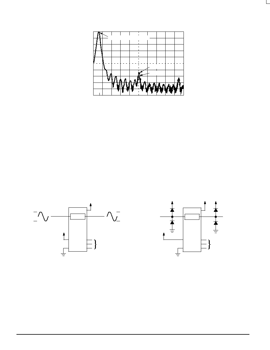
THD
ŒŒŒŒŒŒŒŒŒŒ
ŒŒŒŒŒŒŒŒŒŒ
ŒŒŒŒŒŒŒŒŒŒ
ŒŒŒŒŒŒŒŒŒŒ
ŒŒŒŒŒŒŒŒŒŒ
ŒŒŒŒŒŒŒŒŒŒ
ŒŒŒŒŒŒŒŒŒŒ
Total Harmonic Distortion
(Figure 14)
ŒŒŒŒŒŒŒŒŒŒŒŒŒŒ
ŒŒŒŒŒŒŒŒŒŒŒŒŒŒ
ŒŒŒŒŒŒŒŒŒŒŒŒŒŒ
ŒŒŒŒŒŒŒŒŒŒŒŒŒŒ
ŒŒŒŒŒŒŒŒŒŒŒŒŒŒ
ŒŒŒŒŒŒŒŒŒŒŒŒŒŒ
ŒŒŒŒŒŒŒŒŒŒŒŒŒŒ
fin = 1 kHz, RL = 10 k
, CL = 50 pF
THD = THDMeasured ≠ THDSource
VIS = 4.0 VPP sine wave
VIS = 8.0 VPP sine wave
VIS = 11.0 VPP sine wave
ŒŒŒ
ŒŒŒ
ŒŒŒ
ŒŒŒ
ŒŒŒ
ŒŒŒ
ŒŒŒ
4.5
9.0
12.0
ŒŒŒŒ
ŒŒŒŒ
ŒŒŒŒ
ŒŒŒŒ
ŒŒŒŒ
ŒŒŒŒ
ŒŒŒŒ
0.10
0.06
0.04
ŒŒŒ
ŒŒŒ
ŒŒŒ
ŒŒŒ
ŒŒŒ
ŒŒŒ
ŒŒŒ
%
* Guaranteed limits not tested. Determined by design and verified by qualification.
MC54/74HC4066
High≠Speed CMOS Logic Data
DL129 -- Rev 6
5
MOTOROLA
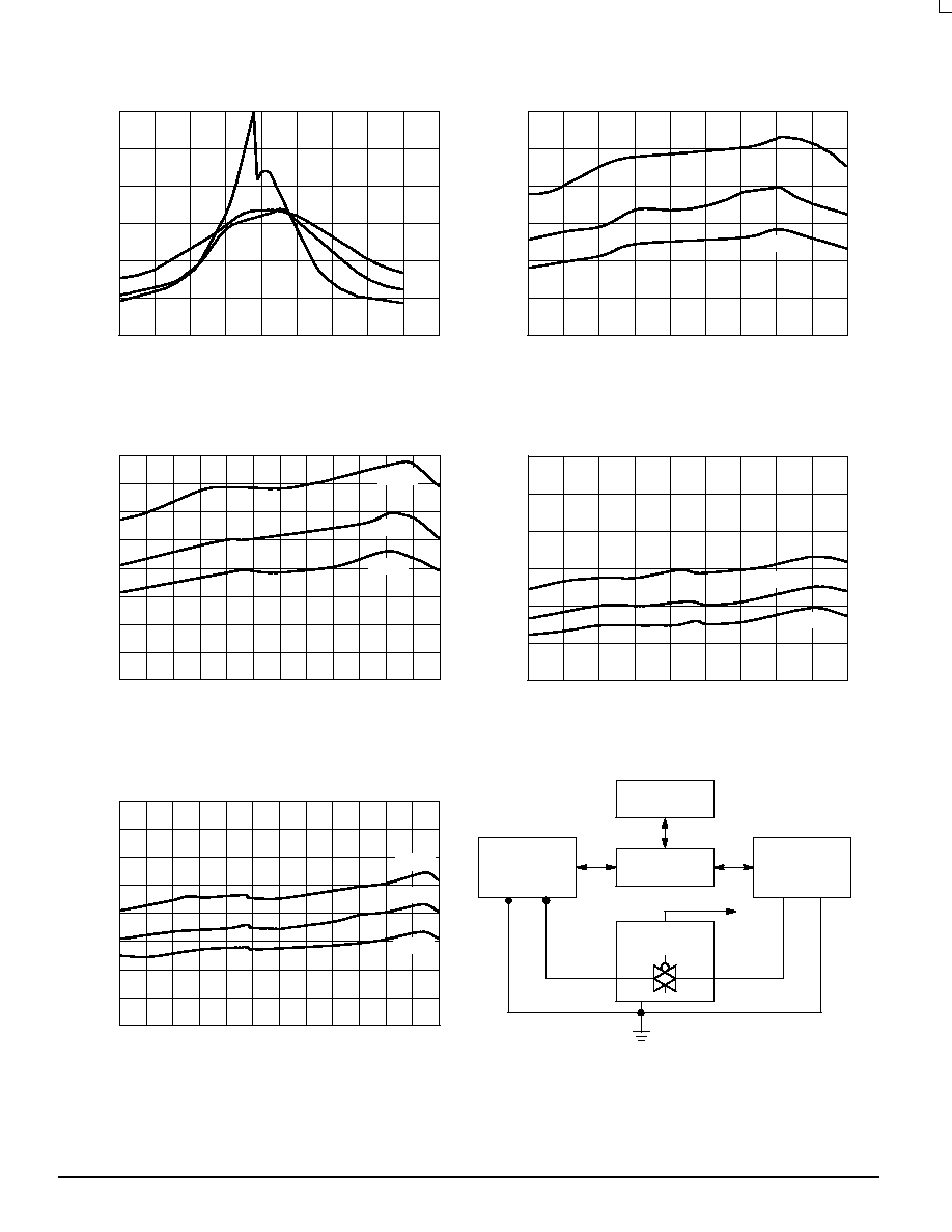
Figure 1a. Typical On Resistance, VCC = 2.0 V
Figure 1b. Typical On Resistance, VCC = 4.5 V
600
500
400
300
200
100
0
2.00
1.75
1.50
1.25
1.00
0.75
0.50
0.25
0
Vin, INPUT VOLTAGE (VOLTS), REFERENCED TO GND
≠ 55
∞
C
25
∞
C
125
∞
C
R
on
, ON RESIST
ANCE (OHMS)
120
100
80
60
40
20
0
4.5
4.0
3.5
3.0
2.5
2.0
1.5
1.0
0.5
0
Vin, INPUT VOLTAGE (VOLTS), REFERENCED TO GND
R
on
, ON RESIST
ANCE (OHMS)
125
∞
C
25
∞
C
≠ 55
∞
C
80
70
60
50
40
30
20
10
0
6.0
5.5
5.0
4.5
4.0
3.5
3.0
2.5
2.0
1.5
1.0
0.5
0
Figure 1c. Typical On Resistance, VCC = 6.0 V
Vin, INPUT VOLTAGE (VOLTS), REFERENCED TO GND
R
on
, ON RESIST
ANCE (OHMS)
125
∞
C
25
∞
C
≠ 55
∞
C
120
100
80
60
40
20
0
9.0
8.0
7.0
6.0
5.0
4.0
3.0
2.0
1.0
0
Figure 1d. Typical On Resistance, VCC = 9.0 V
Vin, INPUT VOLTAGE (VOLTS), REFERENCED TO GND
R
on
, ON RESIST
ANCE (OHMS)
125
∞
C
25
∞
C
≠ 55
∞
C
80
70
60
50
40
30
20
10
0
12
11
10
9.0
8.0
7.0
6.0
5.0
4.0
3.0
2.0
1.0
0
R
on
, ON RESIST
ANCE (OHMS)
Figure 1e. Typical On Resistance, VCC = 12 V
Vin, INPUT VOLTAGE (VOLTS), REFERENCED TO GND
Figure 2. On Resistance Test Set≠Up
PLOTTER
MINI COMPUTER
PROGRAMMABLE
POWER
SUPPLY
DC ANALYZER
VCC
+
≠
ANALOG IN
COMMON OUT
GND
DEVICE
UNDER TEST
125
∞
C
25
∞
C
≠ 55
∞
C

MC54/74HC4066
MOTOROLA
High≠Speed CMOS Logic Data
DL129 -- Rev 6
6
Figure 3. Maximum Off Channel Leakage Current,
Any One Channel, Test Set≠Up
OFF
7
14
VCC
A
VCC
GND
VCC
SELECTED
CONTROL
INPUT
VIL
Figure 4. Maximum On Channel Leakage Current,
Test Set≠Up
ON
14
VCC
N/C
A
GND
VCC
7
SELECTED
CONTROL
INPUT
VIH
Figure 5. Maximum On≠Channel Bandwidth
Test Set≠Up
ON
14
VCC
0.1
µ
F
CL*
fin
dB
METER
*Includes all probe and jig capacitance.
VOS
7
SELECTED
CONTROL
INPUT
VCC
Figure 6. Off≠Channel Feedthrough Isolation,
Test Set≠Up
OFF
7
14
VCC
0.1
µ
F
CL*
fin
dB
METER
*Includes all probe and jig capacitance.
VOS
RL
VIS
SELECTED
CONTROL
INPUT
Figure 7. Feedthrough Noise, ON/OFF Control to
Analog Out, Test Set≠Up
14
VCC
CL*
*Includes all probe and jig capacitance.
OFF/ON
VCC
GND
Vin
1 MHz
tr = tf = 6 ns
CONTROL
VCC/2
RL
IS
RL
VOS
7
SELECTED
CONTROL
INPUT
VCC/2
VCC
GND
ANALOG IN
ANALOG OUT
50%
tPLH
tPHL
50%
Figure 8. Propagation Delays, Analog In to
Analog Out

MC54/74HC4066
High≠Speed CMOS Logic Data
DL129 -- Rev 6
7
MOTOROLA
POSITION
WHEN TESTING tPLZ AND tPZL
Figure 9. Propagation Delay Test Set≠Up
ON
14
VCC
*Includes all probe and jig capacitance.
TEST
POINT
ANALOG OUT
ANALOG IN
CL*
7
SELECTED
CONTROL
INPUT
VCC
tr
tf
VCC
GND
HIGH
IMPEDANCE
VOL
VOH
HIGH
IMPEDANCE
CONTROL
ANALOG
OUT
90%
50%
10%
50%
50%
10%
90%
tPZH
tPHZ
tPZL
tPLZ
Figure 10. Propagation Delay, ON/OFF Control
to Analog Out
ON/OFF
VCC
TEST
POINT
14
VCC
1 k
POSITION
WHEN TESTING tPHZ AND tPZH
CL*
1
2
1
2
Figure 11. Propagation Delay Test Set≠Up
1
2
7
SELECTED
CONTROL
INPUT
Figure 12. Crosstalk Between Any Two Switches,
Test Set≠Up
RL
ON
14
VCC OR GND
CL*
*Includes all probe and jig capacitance.
OFF
RL
RL
VIS
RL
CL*
VOS
fin
0.1
µ
F
VCC/2
VCC/2
7
SELECTED
CONTROL
INPUT
VCC/2
Figure 13. Power Dissipation Capacitance
Test Set≠Up
14
VCC
N/C
OFF/ON
A
N/C
7
SELECTED
CONTROL
INPUT
ON/OFF CONTROL
ON
VCC
0.1
µ
F
CL*
fin
RL
TO
DISTORTION
METER
*Includes all probe and jig capacitance.
VOS
VIS
7
SELECTED
CONTROL
INPUT
VCC
Figure 14. Total Harmonic Distortion, Test Set≠Up
*Includes all probe and jig capacitance.
VCC
VCC/2
MC54/74HC4066
MOTOROLA
High≠Speed CMOS Logic Data
DL129 -- Rev 6
8
0
≠ 10
≠ 20
≠ 30
≠ 40
≠ 50
1.0
2.0
FREQUENCY (kHz)
dBm
≠ 60
≠ 70
≠ 80
≠ 90
FUNDAMENTAL FREQUENCY
DEVICE
SOURCE
Figure 15. Plot, Harmonic Distortion
3.0
APPLICATION INFORMATION
The ON/OFF Control pins should be at VCC or GND logic
levels, VCC being recognized as logic high and GND being
recognized as a logic low. Unused analog inputs/outputs
may be left floating (not connected). However, it is advisable
to tie unused analog inputs and outputs to VCC or GND
through a low value resistor. This minimizes crosstalk and
feedthrough noise that may be picked≠up by the unused I/O
pins.
The maximum analog voltage swings are determined by
the supply voltages VCC and GND. The positive peak analog
voltage should not exceed VCC. Similarly, the negative peak
analog voltage should not go below GND. In the example
below, the difference between VCC and GND is twelve volts.
Therefore, using the configuration in Figure 16, a maximum
analog signal of twelve volts peak≠to≠peak can be con-
trolled.
When voltage transients above VCC and/or below GND
are anticipated on the analog channels, external diodes (Dx)
are recommended as shown in Figure 17. These diodes
should be small signal, fast turn≠on types able to absorb the
maximum anticipated current surges during clipping. An
alternate method would be to replace the Dx diodes with
MO
sorbs (Motorola high current surge protectors).
MO
sorbs are fast turn≠on devices ideally suited for precise
DC protection with no inherent wear out mechanism.
ANALOG O/I
ON
14
VCC = 12 V
ANALOG I/O
+ 12 V
0 V
+ 12 V
0 V
OTHER CONTROL
INPUTS
(VCC OR GND)
ON
16
VCC
Dx
Dx
VCC
Dx
Figure 16. 12 V Application
Figure 17. Transient Suppressor Application
7
SELECTED
CONTROL
INPUT
Dx
OTHER CONTROL
INPUTS
(VCC OR GND)
7
SELECTED
CONTROL
INPUT
VCC

MC54/74HC4066
High≠Speed CMOS Logic Data
DL129 -- Rev 6
9
MOTOROLA
+ 5 V
14
HC4016
CONTROL
INPUTS
7
5
6
14
15
LSTTL/
NMOS
ANALOG
SIGNALS
R*
R* R*
R*
ANALOG
SIGNALS
HCT
BUFFER
R* = 2 TO 10 k
VDD = 5 V
VCC = 5 TO 12 V
ANALOG
SIGNALS
ANALOG
SIGNALS
1
16
14
HC4016
CONTROL
INPUTS
7
8
MC14504
13
3
5
7
9
11
14
2
4
6
10
5
6
14
15
CHANNEL 4
CHANNEL 3
CHANNEL 2
CHANNEL 1
1 OF 4
SWITCHES
COMMON I/O
1
2
3
4
CONTROL INPUTS
INPUT
OUTPUT
0.01
µ
F
LF356 OR
EQUIVALENT
a. Using Pull-Up Resistors
b. Using HCT Buffer
Figure 18. LSTTL/NMOS to HCMOS Interface
Figure 19. TTL/NMOS≠to≠CMOS Level Converter
Analog Signal Peak≠to≠Peak Greater than 5 V
(Also see HC4316)
Figure 20. 4≠Input Multiplexer
Figure 21. Sample/Hold Amplifier
+
≠
1 OF 4
SWITCHES
+ 5 V
14
HC4016
CONTROL
INPUTS
7
5
6
14
15
LSTTL/
NMOS
ANALOG
SIGNALS
ANALOG
SIGNALS
1 OF 4
SWITCHES
1 OF 4
SWITCHES
1 OF 4
SWITCHES

MC54/74HC4066
MOTOROLA
High≠Speed CMOS Logic Data
DL129 -- Rev 6
10
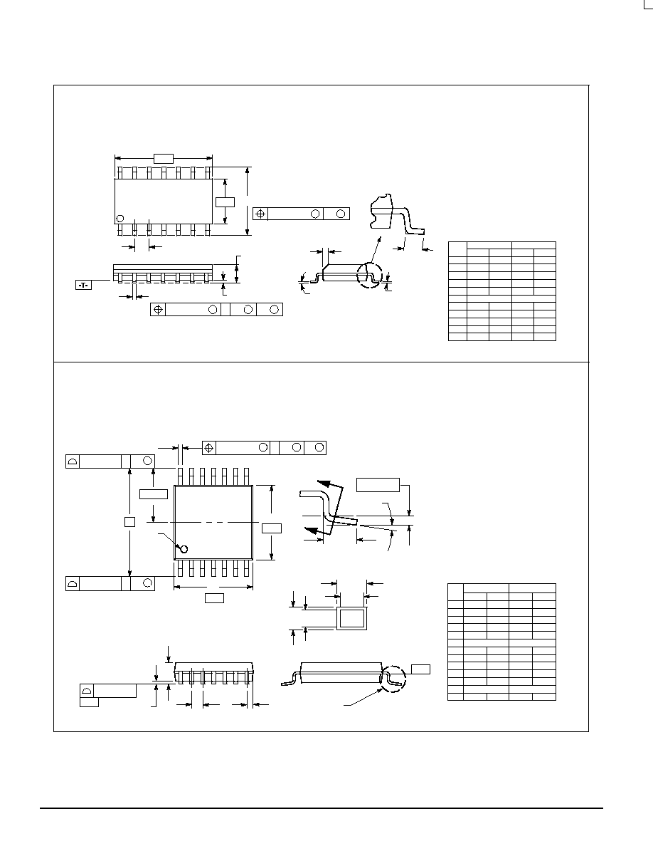
OUTLINE DIMENSIONS
J SUFFIX
CERAMIC DIP PACKAGE
CASE 632≠08
ISSUE Y
MIN
MIN
MAX
MAX
INCHES
MILLIMETERS
DIM
A
B
C
D
F
G
J
K
L
M
N
0.785
0.280
0.200
0.020
0.065
0.015
0.170
15
∞
0.040
0.750
0.245
0.155
0.015
0.055
0.008
0.125
0
∞
0.020
19.94
7.11
5.08
0.50
1.65
0.38
4.31
15
∞
1.01
19.05
6.23
3.94
0.39
1.40
0.21
3.18
0
∞
0.51
0.100 BSC
0.300 BSC
2.54 BSC
7.62 BSC
NOTES:
1. DIMENSIONING AND TOLERANCING PER ANSI
Y14.5M, 1982.
2. CONTROLLING DIMENSION: INCH.
3. DIMENSION L TO CENTER OF LEAD WHEN
FORMED PARALLEL.
4. DIMESNION F MAY NARROW TO 0.76 (0.030)
WHERE THE LEAD ENTERS THE CERAMIC
BODY.
14
8
1
7
-A-
-B-
-T-
SEATING
PLANE
F
G
N
K
C
L
M
0.25 (0.010)
T
A
M
S
0.25 (0.010)
T
B
M
S
J
14 PL
D
14 PL
N SUFFIX
PLASTIC DIP PACKAGE
CASE 646≠06
ISSUE L
NOTES:
1. LEADS WITHIN 0.13 (0.005) RADIUS OF TRUE
POSITION AT SEATING PLANE AT MAXIMUM
MATERIAL CONDITION.
2. DIMENSION L TO CENTER OF LEADS WHEN
FORMED PARALLEL.
3. DIMENSION B DOES NOT INCLUDE MOLD
FLASH.
4. ROUNDED CORNERS OPTIONAL.
1
7
14
8
B
A
F
H
G
D
K
C
N
L
J
M
SEATING
PLANE
DIM
MIN
MAX
MIN
MAX
MILLIMETERS
INCHES
A
0.715
0.770
18.16
19.56
B
0.240
0.260
6.10
6.60
C
0.145
0.185
3.69
4.69
D
0.015
0.021
0.38
0.53
F
0.040
0.070
1.02
1.78
G
0.100 BSC
2.54 BSC
H
0.052
0.095
1.32
2.41
J
0.008
0.015
0.20
0.38
K
0.115
0.135
2.92
3.43
L
0.300 BSC
7.62 BSC
M
0
10
0
10
N
0.015
0.039
0.39
1.01
_
_
_
_
MC54/74HC4066
High≠Speed CMOS Logic Data
DL129 -- Rev 6
11
MOTOROLA
OUTLINE DIMENSIONS
D SUFFIX
PLASTIC SOIC PACKAGE
CASE 751A≠03
ISSUE F
MIN
MIN
MAX
MAX
MILLIMETERS
INCHES
DIM
A
B
C
D
F
G
J
K
M
P
R
8.55
3.80
1.35
0.35
0.40
0.19
0.10
0
∞
5.80
0.25
8.75
4.00
1.75
0.49
1.25
0.25
0.25
7
∞
6.20
0.50
0.337
0.150
0.054
0.014
0.016
0.008
0.004
0
∞
0.228
0.010
0.344
0.157
0.068
0.019
0.049
0.009
0.009
7
∞
0.244
0.019
1.27 BSC
0.050 BSC
NOTES:
1. DIMENSIONING AND TOLERANCING PER ANSI
Y14.5M, 1982.
2. CONTROLLING DIMENSION: MILLIMETER.
3. DIMENSIONS A AND B DO NOT INCLUDE
MOLD PROTRUSION.
4. MAXIMUM MOLD PROTRUSION 0.15 (0.006)
PER SIDE.
5. DIMENSION D DOES NOT INCLUDE DAMBAR
PROTRUSION. ALLOWABLE DAMBAR
PROTRUSION SHALL BE 0.127 (0.005) TOTAL
IN EXCESS OF THE D DIMENSION AT
MAXIMUM MATERIAL CONDITION.
≠A≠
≠B≠
P
7 PL
G
C
K
SEATING
PLANE
D
14 PL
M
J
R
X 45
∞
1
7
8
14
0.25 (0.010)
T
B
A
M
S
S
B
0.25 (0.010)
M
M
F
DT SUFFIX
PLASTIC TSSOP PACKAGE
CASE 948G≠01
ISSUE O
DIM
MIN
MAX
MIN
MAX
INCHES
MILLIMETERS
A
4.90
5.10
0.193
0.200
B
4.30
4.50
0.169
0.177
C
≠≠≠
1.20
≠≠≠
0.047
D
0.05
0.15
0.002
0.006
F
0.50
0.75
0.020
0.030
G
0.65 BSC
0.026 BSC
H
0.50
0.60
0.020
0.024
J
0.09
0.20
0.004
0.008
J1
0.09
0.16
0.004
0.006
K
0.19
0.30
0.007
0.012
K1
0.19
0.25
0.007
0.010
L
6.40 BSC
0.252 BSC
M
0
8
0
8
NOTES:
1. DIMENSIONING AND TOLERANCING PER ANSI
Y14.5M, 1982.
2. CONTROLLING DIMENSION: MILLIMETER.
3. DIMENSION A DOES NOT INCLUDE MOLD FLASH,
PROTRUSIONS OR GATE BURRS. MOLD FLASH
OR GATE BURRS SHALL NOT EXCEED 0.15
(0.006) PER SIDE.
4. DIMENSION B DOES NOT INCLUDE INTERLEAD
FLASH OR PROTRUSION. INTERLEAD FLASH OR
PROTRUSION SHALL NOT EXCEED
0.25 (0.010) PER SIDE.
5. DIMENSION K DOES NOT INCLUDE DAMBAR
PROTRUSION. ALLOWABLE DAMBAR
PROTRUSION SHALL BE 0.08 (0.003) TOTAL IN
EXCESS OF THE K DIMENSION AT MAXIMUM
MATERIAL CONDITION.
6. TERMINAL NUMBERS ARE SHOWN FOR
REFERENCE ONLY.
7. DIMENSION A AND B ARE TO BE DETERMINED
AT DATUM PLANE ≠W≠.
_
_
_
_
S
U
0.15 (0.006) T
2X
L/2
S
U
M
0.10 (0.004)
V
S
T
L
≠U≠
SEATING
PLANE
0.10 (0.004)
≠T≠
«««
«««
«««
«««
SECTION N≠N
DETAIL E
J J1
K
K1
………
………
………
………
DETAIL E
F
M
≠W≠
0.25 (0.010)
8
14
7
1
PIN 1
IDENT.
H
G
A
D
C
B
S
U
0.15 (0.006) T
≠V≠
14X REF
K
N
N
MC54/74HC4066
MOTOROLA
High≠Speed CMOS Logic Data
DL129 -- Rev 6
12
How to reach us:
USA/EUROPE: Motorola Literature Distribution;
JAPAN: Nippon Motorola Ltd.; Tatsumi≠SPD≠JLDC, Toshikatsu Otsuki,
P.O. Box 20912; Phoenix, Arizona 85036. 1≠800≠441≠2447
6F Seibu≠Butsuryu≠Center, 3≠14≠2 Tatsumi Koto≠Ku, Tokyo 135, Japan. 03≠3521≠8315
MFAX: RMFAX0@email.sps.mot.com ≠TOUCHTONE (602) 244≠6609
HONG KONG: Motorola Semiconductors H.K. Ltd.; 8B Tai Ping Industrial Park,
INTERNET: http://Design≠NET.com
51 Ting Kok Road, Tai Po, N.T., Hong Kong. 852≠26629298
Motorola reserves the right to make changes without further notice to any products herein. Motorola makes no warranty, representation or guarantee regarding
the suitability of its products for any particular purpose, nor does Motorola assume any liability arising out of the application or use of any product or circuit,
and specifically disclaims any and all liability, including without limitation consequential or incidental damages. "Typical" parameters can and do vary in different
applications. All operating parameters, including "Typicals" must be validated for each customer application by customer's technical experts. Motorola does
not convey any license under its patent rights nor the rights of others. Motorola products are not designed, intended, or authorized for use as components in
systems intended for surgical implant into the body, or other applications intended to support or sustain life, or for any other application in which the failure of
the Motorola product could create a situation where personal injury or death may occur. Should Buyer purchase or use Motorola products for any such
unintended or unauthorized application, Buyer shall indemnify and hold Motorola and its officers, employees, subsidiaries, affiliates, and distributors harmless
against all claims, costs, damages, and expenses, and reasonable attorney fees arising out of, directly or indirectly, any claim of personal injury or death
associated with such unintended or unauthorized use, even if such claim alleges that Motorola was negligent regarding the design or manufacture of the part.
Motorola and
are registered trademarks of Motorola, Inc. Motorola, Inc. is an Equal Opportunity/Affirmative Action Employer.
MC54/74HC4066/D
*MC54/74HC4066/D*
CODELINE