ƒÓÍÛÏÂÌÚýˆËˇ Ë ÓÔËÒýÌˡ www.docs.chipfind.ru

MC68HC08KH12/H
REV. 1.0
68HC08KH12
68HC708KH12
Advance Information
June 7, 1999
Semiconductor Products Sector

Advance Information
Advance Information
MC68HC(7)08KH12
--
Rev. 1.0
ii
MOTOROLA
Motorola reserves the right to make changes without further notice to
any products herein to improve reliability, function or design. Motorola
does not assume any liability arising out of the application or use of any
product or circuit described herein; neither does it convey any license
under its patent rights nor the rights of others. Motorola products are not
designed, intended, or authorized for use as components in systems
intended for surgical implant into the body, or other applications intended
to support or sustain life, or for any other application in which the failure
of the Motorola product could create a situation where personal injury or
death may occur. Should Buyer purchase or use Motorola products for
any such unintended or unauthorized application, Buyer shall indemnify
and hold Motorola and its officers, employees, subsidiaries, affiliates,
and distributors harmless against all claims, costs, damages, and
expenses, and reasonable attorney fees arising out of, directly or
indirectly, any claim of personal injury or death associated with such
unintended or unauthorized use, even if such claim alleges that Motorola
was negligent regarding the design or manufacture of the part.

MC68HC(7)08KH12
--
Rev. 1.0
Advance Information
MOTOROLA
List of Sections
3
Advance Information -- MC68HC(7)08KH12
List of Sections
Section 1. General Description .......................................23
Section 2. Memory Map ...................................................33
Section 3. Random-Access Memory (RAM) ...................45
Section 4. Read-Only Memory (ROM) .............................47
Section 5. Configuration Register (CONFIG) .................49
Section 6. Central Processor Unit (CPU) .......................51
Section 7. System Integration Module (SIM) .................61
Section 8. Clock Generator Module (CGM) ....................87
Section 9. Universal Serial Bus Module (USB) ............113
Section 10. Monitor ROM (MON) ...................................149
Section 11. Timer Interface Module (TIM) ....................161
Section 12. I/O Ports ......................................................183
Section 13. Computer Operating Properly (COP) .......207
Section 14. External Interrupt (IRQ) .............................213
Section 15. Keyboard Interrupt Module (KBI) ..............219
Section 16. Break Module (BREAK) .............................241
Section 17. Preliminary Electrical Specifications .......247
Section 18. Mechanical Specifications ........................259

List of Sections
Advance Information
MC68HC(7)08KH12
--
Rev. 1.0
4
List of Sections
MOTOROLA

MC68HC(7)08KH12
--
Rev. 1.0
Advance Information
MOTOROLA
Table of Contents
5
Advance Information -- MC68HC(7)08KH12
Table of Contents
General Description
1.1
Contents . . . . . . . . . . . . . . . . . . . . . . . . . . . . . . . . . . . . . . . . . . 23
1.2
Introduction . . . . . . . . . . . . . . . . . . . . . . . . . . . . . . . . . . . . . . . . 24
1.3
Features . . . . . . . . . . . . . . . . . . . . . . . . . . . . . . . . . . . . . . . . . . 24
1.4
MCU Block Diagram . . . . . . . . . . . . . . . . . . . . . . . . . . . . . . . . . 26
1.5
Pin Assignments . . . . . . . . . . . . . . . . . . . . . . . . . . . . . . . . . . . . 28
1.5.1
Quad Flat Pack (QFP) Package . . . . . . . . . . . . . . . . . . . . . 28
1.5.2
Power Supply Pins
(V
DDA
, V
SSA
, V
DD1
, V
SS1
, V
DD2
, and V
SS2
) . . . . . . . . . . 29
1.5.3
Oscillator Pins (OSC1 and OSC2) . . . . . . . . . . . . . . . . . . . 30
1.5.4
External Reset Pin (RST) . . . . . . . . . . . . . . . . . . . . . . . . . . 30
1.5.5
External Interrupt Pin (IRQ1/V
PP
) . . . . . . . . . . . . . . . . . . . . 30
1.5.6
USB Data Pins
(DPLUS0≠DPLUS4 and DMINUS0≠DMINUS4). . . . . . . 30
1.5.7
Voltage Regulator Out (REGOUT) . . . . . . . . . . . . . . . . . . . 30
1.5.8
Port A Input/Output (I/O) Pins (PTA7≠PTA0) . . . . . . . . . . . 31
1.5.9
Port B I/O Pins (PTB7≠PTB0) . . . . . . . . . . . . . . . . . . . . . . . 31
1.5.10
Port C I/O Pins (PTC4≠PTC0). . . . . . . . . . . . . . . . . . . . . . . 31
1.5.11
Port D I/O Pins (PTD7/KBD7≠PTD0/KBD0) . . . . . . . . . . . . 31
1.5.12
Port E I/O Pins (PTE4, PTE3/KBE3, PTE2/KBE2/TCH1,
PTE1/KBE1/TCH0, PTE0/KBE0/TCLK) . . . . . . . . . . . . . 31
1.5.13
Port F I/O Pins (PTF7/KBF7≠PTF0/KBF0) . . . . . . . . . . . . . 32
Section 2. Memory Map
2.1
Contents . . . . . . . . . . . . . . . . . . . . . . . . . . . . . . . . . . . . . . . . . . 33
2.2
Introduction . . . . . . . . . . . . . . . . . . . . . . . . . . . . . . . . . . . . . . . . 33

Table of Contents
Advance Information
MC68HC(7)08KH12
--
Rev. 1.0
6
Table of Contents
MOTOROLA
2.3
I/O Section . . . . . . . . . . . . . . . . . . . . . . . . . . . . . . . . . . . . . . . . 35
2.4
Monitor ROM . . . . . . . . . . . . . . . . . . . . . . . . . . . . . . . . . . . . . . 43
Section 3. Random-Access Memory (RAM)
3.1
Contents . . . . . . . . . . . . . . . . . . . . . . . . . . . . . . . . . . . . . . . . . . 45
3.2
Introduction . . . . . . . . . . . . . . . . . . . . . . . . . . . . . . . . . . . . . . . . 45
3.3
Functional Description . . . . . . . . . . . . . . . . . . . . . . . . . . . . . . . 45
Section 4. Read-Only Memory (ROM)
4.1
Contents . . . . . . . . . . . . . . . . . . . . . . . . . . . . . . . . . . . . . . . . . . 47
4.2
Introduction . . . . . . . . . . . . . . . . . . . . . . . . . . . . . . . . . . . . . . . . 47
4.3
Functional Description . . . . . . . . . . . . . . . . . . . . . . . . . . . . . . . 47
Section 5. Configuration Register (CONFIG)
5.1
Contents . . . . . . . . . . . . . . . . . . . . . . . . . . . . . . . . . . . . . . . . . . 49
5.2
Introduction . . . . . . . . . . . . . . . . . . . . . . . . . . . . . . . . . . . . . . . . 49
5.3
Functional Description . . . . . . . . . . . . . . . . . . . . . . . . . . . . . . . 49
Section 6. Central Processor Unit (CPU)
6.1
Contents . . . . . . . . . . . . . . . . . . . . . . . . . . . . . . . . . . . . . . . . . . 51
6.2
Introduction . . . . . . . . . . . . . . . . . . . . . . . . . . . . . . . . . . . . . . . . 51
6.3
Features . . . . . . . . . . . . . . . . . . . . . . . . . . . . . . . . . . . . . . . . . . 52
6.4
CPU Registers . . . . . . . . . . . . . . . . . . . . . . . . . . . . . . . . . . . . . 52
6.4.1
Accumulator (A). . . . . . . . . . . . . . . . . . . . . . . . . . . . . . . . . . 53
6.4.2
Index Register (H:X) . . . . . . . . . . . . . . . . . . . . . . . . . . . . . . 54
6.4.3
Stack Pointer (SP). . . . . . . . . . . . . . . . . . . . . . . . . . . . . . . . 55
6.4.4
Program Counter (PC) . . . . . . . . . . . . . . . . . . . . . . . . . . . . 56
6.4.5
Condition Code Register (CCR) . . . . . . . . . . . . . . . . . . . . . 57
6.5
Arithmetic/Logic Unit (ALU) . . . . . . . . . . . . . . . . . . . . . . . . . . . 59

Table of Contents
MC68HC(7)08KH12
--
Rev. 1.0
Advance Information
MOTOROLA
Table of Contents
7
Section 7. System Integration Module (SIM)
7.1
Contents . . . . . . . . . . . . . . . . . . . . . . . . . . . . . . . . . . . . . . . . . . 61
7.2
Introduction . . . . . . . . . . . . . . . . . . . . . . . . . . . . . . . . . . . . . . . . 62
7.3
SIM Bus Clock Control and Generation . . . . . . . . . . . . . . . . . . 65
7.3.1
Bus Timing . . . . . . . . . . . . . . . . . . . . . . . . . . . . . . . . . . . . . 65
7.3.2
Clock Start-Up from POR . . . . . . . . . . . . . . . . . . . . . . . . . . 66
7.3.3
Clocks in Stop Mode and Wait Mode . . . . . . . . . . . . . . . . . 66
7.4
Reset and System Initialization. . . . . . . . . . . . . . . . . . . . . . . . . 66
7.4.1
External Pin Reset. . . . . . . . . . . . . . . . . . . . . . . . . . . . . . . . 67
7.4.2
Active Resets from Internal Sources . . . . . . . . . . . . . . . . . . 67
7.4.2.1
Power-On Reset . . . . . . . . . . . . . . . . . . . . . . . . . . . . . . . 68
7.4.2.2
Computer Operating Properly (COP) Reset . . . . . . . . . . 69
7.4.2.3
Illegal Opcode Reset . . . . . . . . . . . . . . . . . . . . . . . . . . . . 70
7.4.2.4
Illegal Address Reset . . . . . . . . . . . . . . . . . . . . . . . . . . . . 70
7.4.2.5
Universal Serial Bus Reset . . . . . . . . . . . . . . . . . . . . . . . 70
7.5
SIM Counter . . . . . . . . . . . . . . . . . . . . . . . . . . . . . . . . . . . . . . . 71
7.5.1
SIM Counter During Power-On Reset . . . . . . . . . . . . . . . . . 71
7.5.2
SIM Counter During Stop Mode Recovery . . . . . . . . . . . . . 71
7.5.3
SIM Counter and Reset States . . . . . . . . . . . . . . . . . . . . . . 71
7.6
Exception Control . . . . . . . . . . . . . . . . . . . . . . . . . . . . . . . . . . . 72
7.6.1
Interrupts . . . . . . . . . . . . . . . . . . . . . . . . . . . . . . . . . . . . . . . 72
7.6.1.1
Hardware Interrupts . . . . . . . . . . . . . . . . . . . . . . . . . . . . . 74
7.6.1.2
SWI Instruction. . . . . . . . . . . . . . . . . . . . . . . . . . . . . . . . . 76
7.6.2
Interrupt Status Registers . . . . . . . . . . . . . . . . . . . . . . . . . . 76
7.6.2.1
Interrupt Status Register 1 . . . . . . . . . . . . . . . . . . . . . . . . 77
7.6.2.2
Interrupt Status Register 2 . . . . . . . . . . . . . . . . . . . . . . . . 78
7.6.2.3
Interrupt Status Register 3 . . . . . . . . . . . . . . . . . . . . . . . . 78
7.6.3
Reset . . . . . . . . . . . . . . . . . . . . . . . . . . . . . . . . . . . . . . . . . . 79
7.6.4
Break Interrupts. . . . . . . . . . . . . . . . . . . . . . . . . . . . . . . . . . 79
7.6.5
Status Flag Protection in Break Mode. . . . . . . . . . . . . . . . . 79
7.7
Low-Power Modes . . . . . . . . . . . . . . . . . . . . . . . . . . . . . . . . . . 79
7.7.1
Wait Mode . . . . . . . . . . . . . . . . . . . . . . . . . . . . . . . . . . . . . . 80
7.7.2
Stop Mode . . . . . . . . . . . . . . . . . . . . . . . . . . . . . . . . . . . . . . 81
7.8
SIM Registers . . . . . . . . . . . . . . . . . . . . . . . . . . . . . . . . . . . . . . 83
7.8.1
Break Status Register (BSR). . . . . . . . . . . . . . . . . . . . . . . . 83

Table of Contents
Advance Information
MC68HC(7)08KH12
--
Rev. 1.0
8
Table of Contents
MOTOROLA
7.8.2
Reset Status Register (RSR) . . . . . . . . . . . . . . . . . . . . . . . 84
7.8.3
Break Flag Control Register (BFCR). . . . . . . . . . . . . . . . . . 85
Section 8. Clock Generator Module (CGM)
8.1
Contents . . . . . . . . . . . . . . . . . . . . . . . . . . . . . . . . . . . . . . . . . . 87
8.2
Introduction . . . . . . . . . . . . . . . . . . . . . . . . . . . . . . . . . . . . . . . . 88
8.3
Features . . . . . . . . . . . . . . . . . . . . . . . . . . . . . . . . . . . . . . . . . . 89
8.4
Functional Description . . . . . . . . . . . . . . . . . . . . . . . . . . . . . . . 89
8.4.1
Crystal Oscillator Circuit . . . . . . . . . . . . . . . . . . . . . . . . . . . 91
8.4.2
Phase-Locked Loop Circuit (PLL) . . . . . . . . . . . . . . . . . . . . 91
8.4.3
PLL Circuits . . . . . . . . . . . . . . . . . . . . . . . . . . . . . . . . . . . . . 91
8.4.4
Acquisition and Tracking Modes . . . . . . . . . . . . . . . . . . . . . 93
8.4.5
Manual and Automatic PLL Bandwidth Modes . . . . . . . . . . 93
8.4.6
Programming the PLL . . . . . . . . . . . . . . . . . . . . . . . . . . . . . 94
8.4.7
Special Programming Exceptions . . . . . . . . . . . . . . . . . . . . 95
8.4.8
Base Clock Selector Circuit. . . . . . . . . . . . . . . . . . . . . . . . . 96
8.4.9
CGM External Connections. . . . . . . . . . . . . . . . . . . . . . . . . 96
8.5
I/O Signals . . . . . . . . . . . . . . . . . . . . . . . . . . . . . . . . . . . . . . . . 98
8.5.1
Crystal Amplifier Input Pin (OSC1) . . . . . . . . . . . . . . . . . . . 98
8.5.2
Crystal Amplifier Output Pin (OSC2) . . . . . . . . . . . . . . . . . . 98
8.5.3
External Filter Capacitor Pin (CGMXFC). . . . . . . . . . . . . . . 98
8.5.4
PLL Analog Power Pin (V
DDA
) . . . . . . . . . . . . . . . . . . . . . . 98
8.5.5
PLL Analog Ground Pin (V
SSA
) . . . . . . . . . . . . . . . . . . . . . . 98
8.5.6
Buffered Crystal Clock Output (CGMVOUT) . . . . . . . . . . . . 99
8.5.7
CGMVSEL. . . . . . . . . . . . . . . . . . . . . . . . . . . . . . . . . . . . . . 99
8.5.8
Oscillator Enable Signal (SIMOSCEN) . . . . . . . . . . . . . . . . 99
8.5.9
Crystal Output Frequency Signal (CGMXCLK) . . . . . . . . . . 99
8.5.10
CGM Base Clock Output (CGMOUT) . . . . . . . . . . . . . . . . . 99
8.5.11
CGM CPU Interrupt (CGMINT) . . . . . . . . . . . . . . . . . . . . . . 99
8.6
CGM Registers . . . . . . . . . . . . . . . . . . . . . . . . . . . . . . . . . . . . 100
8.6.1
PLL Control Register (PCTL) . . . . . . . . . . . . . . . . . . . . . . 102
8.6.2
PLL Bandwidth Control Register (PBWC) . . . . . . . . . . . . . 104
8.6.3
PLL Multiplier Select Registers (PMSH:PMSL). . . . . . . . . 105
8.6.4
PLL Reference Divider Select Register (PRDS) . . . . . . . . 106

Table of Contents
MC68HC(7)08KH12
--
Rev. 1.0
Advance Information
MOTOROLA
Table of Contents
9
8.7
Interrupts. . . . . . . . . . . . . . . . . . . . . . . . . . . . . . . . . . . . . . . . . 107
8.8
Special Modes . . . . . . . . . . . . . . . . . . . . . . . . . . . . . . . . . . . . 107
8.8.1
Wait Mode . . . . . . . . . . . . . . . . . . . . . . . . . . . . . . . . . . . . . 107
8.8.2
CGM During Break Interrupts . . . . . . . . . . . . . . . . . . . . . . 108
8.9
Acquisition/Lock Time Specifications . . . . . . . . . . . . . . . . . . . 108
8.9.1
Acquisition/Lock Time Definitions . . . . . . . . . . . . . . . . . . . 108
8.9.2
Parametric Influences on Reaction Time . . . . . . . . . . . . . 109
8.9.3
Choosing a Filter Capacitor. . . . . . . . . . . . . . . . . . . . . . . . 111
8.9.4
Reaction Time Calculation . . . . . . . . . . . . . . . . . . . . . . . . 111
Section 9. Universal Serial Bus Module (USB)
9.1
Contents . . . . . . . . . . . . . . . . . . . . . . . . . . . . . . . . . . . . . . . . . 113
9.2
Features . . . . . . . . . . . . . . . . . . . . . . . . . . . . . . . . . . . . . . . . . 114
9.3
Overview. . . . . . . . . . . . . . . . . . . . . . . . . . . . . . . . . . . . . . . . . 115
9.4
I/O Register Description of the HUB function . . . . . . . . . . . . . 116
9.4.1
USB HUB Root Port Control Register (HRPCR) . . . . . . . . 120
9.4.2
USB HUB Downstream Port Control Register
(HDP1CR-HDP4CR) . . . . . . . . . . . . . . . . . . . . . . . . . . 121
9.4.3
USB SIE Timing Interrupt Register (SIETIR). . . . . . . . . . . 123
9.4.4
USB SIE Timing Status Register (SIETSR) . . . . . . . . . . . 125
9.4.5
USB HUB Address Register (HADDR) . . . . . . . . . . . . . . . 127
9.4.6
USB HUB Interrupt Register 0 (HIR0) . . . . . . . . . . . . . . . . 128
9.4.7
USB HUB Control Register 0 (HCR0) . . . . . . . . . . . . . . . . 129
9.4.8
USB HUB Endpoint1 Control & Data Register (HCDR) . . 131
9.4.9
USB HUB Status Register (HSR) . . . . . . . . . . . . . . . . . . . 132
9.4.10
USB HUB Endpoint 0 Data Registers 0-7
(HE0D0-HE0D7). . . . . . . . . . . . . . . . . . . . . . . . . . . . . . 134
9.5
I/O Register Description of the Embedded Device Function . 134
9.5.1
USB Embedded Device Address Register (DADDR) . . . . 138
9.5.2
USB Embedded Device Interrupt Register 0 (DIR0) . . . . . 138
9.5.3
USB Embedded Device Interrupt Register 1 (DIR1) . . . . . 140
9.5.4
USB Embedded Device Control Register 0 (DCR0) . . . . . 141
9.5.5
USB Embedded Device Control Register 1 (DCR1) . . . . . 143
9.5.6
USB Embedded Device Status Register (DSR) . . . . . . . . 144

Table of Contents
Advance Information
MC68HC(7)08KH12
--
Rev. 1.0
10
Table of Contents
MOTOROLA
9.5.7
USB Embedded Device Control Register 2 (DCR2) . . . . . 146
9.5.8
USB Embedded Device Endpoint 0 Data Registers
(DE0D0-DE0D7). . . . . . . . . . . . . . . . . . . . . . . . . . . . . . 147
9.5.9
USB Embedded Device Endpoint 1/2 Data Registers
(DE1D0-DE1D7). . . . . . . . . . . . . . . . . . . . . . . . . . . . . . 148
Section 10. Monitor ROM (MON)
10.1
Contents . . . . . . . . . . . . . . . . . . . . . . . . . . . . . . . . . . . . . . . . . 149
10.2
Introduction . . . . . . . . . . . . . . . . . . . . . . . . . . . . . . . . . . . . . . . 149
10.3
Features . . . . . . . . . . . . . . . . . . . . . . . . . . . . . . . . . . . . . . . . . 150
10.4
Functional Description . . . . . . . . . . . . . . . . . . . . . . . . . . . . . . 150
10.4.1
Entering Monitor Mode . . . . . . . . . . . . . . . . . . . . . . . . . . . 152
10.4.2
Data Format . . . . . . . . . . . . . . . . . . . . . . . . . . . . . . . . . . . 154
10.4.3
Echoing . . . . . . . . . . . . . . . . . . . . . . . . . . . . . . . . . . . . . . . 154
10.4.4
Break Signal . . . . . . . . . . . . . . . . . . . . . . . . . . . . . . . . . . . 155
10.4.5
Commands . . . . . . . . . . . . . . . . . . . . . . . . . . . . . . . . . . . . 155
10.4.6
Baud Rate . . . . . . . . . . . . . . . . . . . . . . . . . . . . . . . . . . . . . 159
Section 11. Timer Interface Module (TIM)
11.1
Contents . . . . . . . . . . . . . . . . . . . . . . . . . . . . . . . . . . . . . . . . . 161
11.2
Introduction . . . . . . . . . . . . . . . . . . . . . . . . . . . . . . . . . . . . . . . 162
11.3
Features . . . . . . . . . . . . . . . . . . . . . . . . . . . . . . . . . . . . . . . . . 162
11.4
Functional Description . . . . . . . . . . . . . . . . . . . . . . . . . . . . . . 163
11.4.1
TIM Counter Prescaler . . . . . . . . . . . . . . . . . . . . . . . . . . . 165
11.4.2
Input Capture. . . . . . . . . . . . . . . . . . . . . . . . . . . . . . . . . . . 165
11.4.3
Output Compare . . . . . . . . . . . . . . . . . . . . . . . . . . . . . . . . 165
11.4.3.1
Unbuffered Output Compare . . . . . . . . . . . . . . . . . . . . . 166
11.4.3.2
Buffered Output Compare . . . . . . . . . . . . . . . . . . . . . . . 166
11.4.4
Pulse Width Modulation (PWM) . . . . . . . . . . . . . . . . . . . . 167
11.4.4.1
Unbuffered PWM Signal Generation . . . . . . . . . . . . . . . 168
11.4.4.2
Buffered PWM Signal Generation . . . . . . . . . . . . . . . . . 169
11.4.4.3
PWM Initialization . . . . . . . . . . . . . . . . . . . . . . . . . . . . . 170
11.5
Interrupts. . . . . . . . . . . . . . . . . . . . . . . . . . . . . . . . . . . . . . . . . 171

Table of Contents
MC68HC(7)08KH12
--
Rev. 1.0
Advance Information
MOTOROLA
Table of Contents
11
11.6
Wait Mode. . . . . . . . . . . . . . . . . . . . . . . . . . . . . . . . . . . . . . . . 171
11.7
TIM During Break Interrupts . . . . . . . . . . . . . . . . . . . . . . . . . . 172
11.8
I/O Signals . . . . . . . . . . . . . . . . . . . . . . . . . . . . . . . . . . . . . . . 172
11.8.1
TIM Clock Pin (PTE0/TCLK) . . . . . . . . . . . . . . . . . . . . . . . 172
11.8.2
TIM Channel I/O Pins (PTE1/TCH0:PTE2/TCH1). . . . . . . 173
11.9
I/O Registers. . . . . . . . . . . . . . . . . . . . . . . . . . . . . . . . . . . . . . 173
11.9.1
TIM Status and Control Register (TSC) . . . . . . . . . . . . . . 173
11.9.2
TIM Counter Registers (TCNTH:TCNTL) . . . . . . . . . . . . . 175
11.9.3
TIM Counter Modulo Registers (TMODH:TMODL) . . . . . . 176
11.9.4
TIM Channel Status and Control Registers (TSC0:TSC1) 177
11.9.5
TIM Channel Registers (TCH0H/L≠TCH1H/L) . . . . . . . . . 181
Section 12. I/O Ports
12.1
Contents . . . . . . . . . . . . . . . . . . . . . . . . . . . . . . . . . . . . . . . . . 183
12.2
Introduction . . . . . . . . . . . . . . . . . . . . . . . . . . . . . . . . . . . . . . . 184
12.3
Port A . . . . . . . . . . . . . . . . . . . . . . . . . . . . . . . . . . . . . . . . . . . 186
12.3.1
Port A Data Register (PTA) . . . . . . . . . . . . . . . . . . . . . . . . 186
12.3.2
Data Direction Register A (DDRA) . . . . . . . . . . . . . . . . . . 186
12.4
Port B . . . . . . . . . . . . . . . . . . . . . . . . . . . . . . . . . . . . . . . . . . . 188
12.4.1
Port B Data Register (PTB) . . . . . . . . . . . . . . . . . . . . . . . . 188
12.4.2
Data Direction Register B (DDRB) . . . . . . . . . . . . . . . . . . 189
12.5
Port C . . . . . . . . . . . . . . . . . . . . . . . . . . . . . . . . . . . . . . . . . . . 190
12.5.1
Port C Data Register (PTC). . . . . . . . . . . . . . . . . . . . . . . . 190
12.5.2
Data Direction Register C (DDRC) . . . . . . . . . . . . . . . . . . 191
12.6
Port D . . . . . . . . . . . . . . . . . . . . . . . . . . . . . . . . . . . . . . . . . . . 192
12.6.1
Port D Data Register (PTD). . . . . . . . . . . . . . . . . . . . . . . . 193
12.6.2
Data Direction Register D (DDRD) . . . . . . . . . . . . . . . . . . 193
12.7
Port E . . . . . . . . . . . . . . . . . . . . . . . . . . . . . . . . . . . . . . . . . . . 195
12.7.1
Port E Data Register (PTE) . . . . . . . . . . . . . . . . . . . . . . . . 195
12.7.2
Data Direction Register E (DDRE) . . . . . . . . . . . . . . . . . . 196
12.7.3
Port-E Optical Interface Enable Register . . . . . . . . . . . . . 198
12.8
Port F . . . . . . . . . . . . . . . . . . . . . . . . . . . . . . . . . . . . . . . . . . . 202

Table of Contents
Advance Information
MC68HC(7)08KH12
--
Rev. 1.0
12
Table of Contents
MOTOROLA
12.8.1
Port F Data Register (PTF) . . . . . . . . . . . . . . . . . . . . . . . . 202
12.8.2
Data Direction Register F (DDRF). . . . . . . . . . . . . . . . . . . 203
12.9
Port Options . . . . . . . . . . . . . . . . . . . . . . . . . . . . . . . . . . . . . . 204
12.9.1
Port Option Control Register (POC) . . . . . . . . . . . . . . . . . 204
Section 13. Computer Operating Properly (COP)
13.1
Contents . . . . . . . . . . . . . . . . . . . . . . . . . . . . . . . . . . . . . . . . . 207
13.2
Introduction . . . . . . . . . . . . . . . . . . . . . . . . . . . . . . . . . . . . . . . 207
13.3
Functional Description . . . . . . . . . . . . . . . . . . . . . . . . . . . . . . 208
13.4
I/O Signals . . . . . . . . . . . . . . . . . . . . . . . . . . . . . . . . . . . . . . . 209
13.4.1
CGMXCLK. . . . . . . . . . . . . . . . . . . . . . . . . . . . . . . . . . . . . 209
13.4.2
COPCTL Write . . . . . . . . . . . . . . . . . . . . . . . . . . . . . . . . . 209
13.4.3
Power-On Reset . . . . . . . . . . . . . . . . . . . . . . . . . . . . . . . . 210
13.4.4
Internal Reset . . . . . . . . . . . . . . . . . . . . . . . . . . . . . . . . . . 210
13.4.5
Reset Vector Fetch . . . . . . . . . . . . . . . . . . . . . . . . . . . . . . 210
13.4.6
COPD (COP Disable) . . . . . . . . . . . . . . . . . . . . . . . . . . . . 210
13.4.7
COPRS (COP Rate Select). . . . . . . . . . . . . . . . . . . . . . . . 210
13.5
COP Control Register (COPCTL) . . . . . . . . . . . . . . . . . . . . . . 211
13.6
Interrupts. . . . . . . . . . . . . . . . . . . . . . . . . . . . . . . . . . . . . . . . . 211
13.7
Monitor Mode . . . . . . . . . . . . . . . . . . . . . . . . . . . . . . . . . . . . . 211
13.8
Low-Power Modes . . . . . . . . . . . . . . . . . . . . . . . . . . . . . . . . . 212
13.8.1
Wait Mode . . . . . . . . . . . . . . . . . . . . . . . . . . . . . . . . . . . . . 212
13.8.2
Stop Mode . . . . . . . . . . . . . . . . . . . . . . . . . . . . . . . . . . . . . 212
13.9
COP Module During Break Mode . . . . . . . . . . . . . . . . . . . . . . 212
Section 14. External Interrupt (IRQ)
14.1
Contents . . . . . . . . . . . . . . . . . . . . . . . . . . . . . . . . . . . . . . . . . 213
14.2
Introduction . . . . . . . . . . . . . . . . . . . . . . . . . . . . . . . . . . . . . . . 213
14.3
Features . . . . . . . . . . . . . . . . . . . . . . . . . . . . . . . . . . . . . . . . . 213
14.4
Functional Description . . . . . . . . . . . . . . . . . . . . . . . . . . . . . . 214

Table of Contents
MC68HC(7)08KH12
--
Rev. 1.0
Advance Information
MOTOROLA
Table of Contents
13
14.4.1
IRQ1/V
PP
Pin . . . . . . . . . . . . . . . . . . . . . . . . . . . . . . . . . . . 215
14.5
IRQ Module During Break Interrupts . . . . . . . . . . . . . . . . . . . 217
14.6
IRQ Status and Control Register (ISCR) . . . . . . . . . . . . . . . . 217
Section 15. Keyboard Interrupt Module (KBI)
15.1
Contents . . . . . . . . . . . . . . . . . . . . . . . . . . . . . . . . . . . . . . . . . 219
15.2
Introduction . . . . . . . . . . . . . . . . . . . . . . . . . . . . . . . . . . . . . . . 220
15.3
Features . . . . . . . . . . . . . . . . . . . . . . . . . . . . . . . . . . . . . . . . . 220
15.4
Port-D Keyboard Interrupt Block Diagram . . . . . . . . . . . . . . . 222
15.4.1
Port-D Keyboard Interrupt Functional Description. . . . . . . 223
15.4.2
Port-D Keyboard Initialization . . . . . . . . . . . . . . . . . . . . . . 224
15.4.3
Port-D Keyboard Interrupt Registers . . . . . . . . . . . . . . . . . 225
15.4.3.1
Port-D Keyboard Status and Control Register: . . . . . . . 225
15.4.3.2
Port-D Keyboard Interrupt Enable Register . . . . . . . . . . 226
15.5
Port-E Keyboard Interrupt Block Diagram . . . . . . . . . . . . . . . 228
15.5.1
Port-E Keyboard Interrupt Functional Description. . . . . . . 229
15.5.2
Port-E Keyboard Initialization . . . . . . . . . . . . . . . . . . . . . . 230
15.5.3
Port-E Keyboard Interrupt Registers . . . . . . . . . . . . . . . . . 231
15.5.3.1
Port-E Keyboard Status and Control Register . . . . . . . . 231
15.5.3.2
Port-E Keyboard Interrupt Enable Register . . . . . . . . . . 232
15.6
Port-F Keyboard Interrupt Block Diagram. . . . . . . . . . . . . . . . 234
15.6.1
Port-F Keyboard Interrupt Functional Description . . . . . . . 235
15.6.2
Port-F Keyboard Initialization . . . . . . . . . . . . . . . . . . . . . . 236
15.6.3
Port-F Keyboard Interrupt Registers . . . . . . . . . . . . . . . . . 237
15.6.3.1
Port-F Keyboard Status and Control Register . . . . . . . . 237
15.6.3.2
Port-F Keyboard Interrupt Enable Register . . . . . . . . . . 238
15.6.3.3
Port-F Pull-up Enable Register . . . . . . . . . . . . . . . . . . . 239
15.7
Wait Mode. . . . . . . . . . . . . . . . . . . . . . . . . . . . . . . . . . . . . . . . 239
15.8
Stop Mode . . . . . . . . . . . . . . . . . . . . . . . . . . . . . . . . . . . . . . . 239
15.9
Keyboard Module During Break Interrupts . . . . . . . . . . . . . . . 239

Table of Contents
Advance Information
MC68HC(7)08KH12
--
Rev. 1.0
14
Table of Contents
MOTOROLA
Section 16. Break Module (BREAK)
16.1
Contents . . . . . . . . . . . . . . . . . . . . . . . . . . . . . . . . . . . . . . . . . 241
16.2
Introduction . . . . . . . . . . . . . . . . . . . . . . . . . . . . . . . . . . . . . . . 241
16.3
Features . . . . . . . . . . . . . . . . . . . . . . . . . . . . . . . . . . . . . . . . . 242
16.4
Functional Description . . . . . . . . . . . . . . . . . . . . . . . . . . . . . . 242
16.4.1
Flag Protection During Break Interrupts . . . . . . . . . . . . . . 244
16.4.2
CPU During Break Interrupts. . . . . . . . . . . . . . . . . . . . . . . 244
16.4.3
TIM During Break Interrupts . . . . . . . . . . . . . . . . . . . . . . . 244
16.4.4
COP During Break Interrupts . . . . . . . . . . . . . . . . . . . . . . 244
16.5
Break Module Registers . . . . . . . . . . . . . . . . . . . . . . . . . . . . . 244
16.5.1
Break Status and Control Register (BRKSCR) . . . . . . . . . 245
16.5.2
Break Address Registers (BRKH and BRKL) . . . . . . . . . . 245
16.6
Low-Power Modes . . . . . . . . . . . . . . . . . . . . . . . . . . . . . . . . . 246
16.6.1
Wait Mode . . . . . . . . . . . . . . . . . . . . . . . . . . . . . . . . . . . . . 246
16.6.2
Stop Mode . . . . . . . . . . . . . . . . . . . . . . . . . . . . . . . . . . . . . 246
Section 17. Preliminary Electrical Specifications
17.1
Contents . . . . . . . . . . . . . . . . . . . . . . . . . . . . . . . . . . . . . . . . . 247
17.2
Introduction . . . . . . . . . . . . . . . . . . . . . . . . . . . . . . . . . . . . . . . 247
17.3
Absolute Maximum Ratings . . . . . . . . . . . . . . . . . . . . . . . . . . 248
17.4
Functional Operating Range. . . . . . . . . . . . . . . . . . . . . . . . . . 249
17.5
Thermal Characteristics . . . . . . . . . . . . . . . . . . . . . . . . . . . . . 249
17.6
DC Electrical Characteristics . . . . . . . . . . . . . . . . . . . . . . . . . 250
17.7
Control Timing . . . . . . . . . . . . . . . . . . . . . . . . . . . . . . . . . . . . 251
17.8
Oscillator Characteristics . . . . . . . . . . . . . . . . . . . . . . . . . . . . 251
17.9
USB DC Electrical Characteristics . . . . . . . . . . . . . . . . . . . . . 252
17.10 USB Low Speed Source Electrical Characteristics. . . . . . . . . 253
17.11 USB High Speed Source Electrical Characteristics . . . . . . . . 254

Table of Contents
MC68HC(7)08KH12
--
Rev. 1.0
Advance Information
MOTOROLA
Table of Contents
15
17.12 HUB Repeater Electrical Characteristics . . . . . . . . . . . . . . . . 255
17.13 USB Signaling Levels . . . . . . . . . . . . . . . . . . . . . . . . . . . . . . . 256
17.14 TImer Interface Module Characteristics . . . . . . . . . . . . . . . . . 256
17.15 Clock Generation Module Characteristics . . . . . . . . . . . . . . . 257
17.15.1
CGM Component Specifications . . . . . . . . . . . . . . . . . . . . 257
17.15.2
CGM Electrical Specifications . . . . . . . . . . . . . . . . . . . . . . 257
17.15.3
Acquisition/Lock Time Specifications . . . . . . . . . . . . . . . . 258
Section 18. Mechanical Specifications
18.1
Contents . . . . . . . . . . . . . . . . . . . . . . . . . . . . . . . . . . . . . . . . . 259
18.2
Introduction . . . . . . . . . . . . . . . . . . . . . . . . . . . . . . . . . . . . . . . 259
18.3
Plastic Quad Flat Pack (QFP). . . . . . . . . . . . . . . . . . . . . . . . . 260

Table of Contents
Advance Information
MC68HC(7)08KH12
--
Rev. 1.0
16
Table of Contents
MOTOROLA

MC68HC(7)08KH12
--
Rev. 1.0
Advance Information
MOTOROLA
List of Figures
17
Advance Information -- MC68HC(7)08KH12
List of Figures
Figure
Title
Page
1-1
MCU Block Diagram . . . . . . . . . . . . . . . . . . . . . . . . . . . . . . . . . 27
1-2
64-Pin QFP Assignments (Top View) . . . . . . . . . . . . . . . . . . . . 28
1-3
Power Supply Bypassing . . . . . . . . . . . . . . . . . . . . . . . . . . . . . 29
2-1
Memory Map. . . . . . . . . . . . . . . . . . . . . . . . . . . . . . . . . . . . . . . 34
2-2
Control, Status, and Data Registers . . . . . . . . . . . . . . . . . . . . . 36
5-1
Configuration Register (CONFIG). . . . . . . . . . . . . . . . . . . . . . . 50
6-1
CPU Registers . . . . . . . . . . . . . . . . . . . . . . . . . . . . . . . . . . . . . 53
6-2
Accumulator (A) . . . . . . . . . . . . . . . . . . . . . . . . . . . . . . . . . . . . 53
6-3
Index Register (H:X) . . . . . . . . . . . . . . . . . . . . . . . . . . . . . . . . . 54
6-4
Stack Pointer (SP) . . . . . . . . . . . . . . . . . . . . . . . . . . . . . . . . . . 55
6-5
Program Counter (PC) . . . . . . . . . . . . . . . . . . . . . . . . . . . . . . . 56
6-6
Condition Code Register (CCR) . . . . . . . . . . . . . . . . . . . . . . . . 57
7-1
SIM Block Diagram . . . . . . . . . . . . . . . . . . . . . . . . . . . . . . . . . . 63
7-2
SIM I/O Register Summary. . . . . . . . . . . . . . . . . . . . . . . . . . . . 64
7-3
SIM Clock Signals. . . . . . . . . . . . . . . . . . . . . . . . . . . . . . . . . . . 65
7-4
External Reset Timing . . . . . . . . . . . . . . . . . . . . . . . . . . . . . . . 67
7-5
Internal Reset Timing . . . . . . . . . . . . . . . . . . . . . . . . . . . . . . . . 68
7-6
Sources of Internal Reset . . . . . . . . . . . . . . . . . . . . . . . . . . . . . 68
7-7
POR Recovery . . . . . . . . . . . . . . . . . . . . . . . . . . . . . . . . . . . . . 69
7-8
Interrupt Processing . . . . . . . . . . . . . . . . . . . . . . . . . . . . . . . . . 73
7-9
Interrupt Entry . . . . . . . . . . . . . . . . . . . . . . . . . . . . . . . . . . . . . . 74
7-10
Interrupt Recovery . . . . . . . . . . . . . . . . . . . . . . . . . . . . . . . . . . 74
7-11
Interrupt Recognition Example . . . . . . . . . . . . . . . . . . . . . . . . . 75
7-12
Interrupt Status Register 1 (INT1). . . . . . . . . . . . . . . . . . . . . . . 77
7-13
Interrupt Status Register 2 (INT2). . . . . . . . . . . . . . . . . . . . . . . 78
7-14
Interrupt Status Register 2 (INT2). . . . . . . . . . . . . . . . . . . . . . . 78

List of Figures
Advance Information
MC68HC(7)08KH12
--
Rev. 1.0
18
List of Figures
MOTOROLA
Figure
Title
Page
7-15
Wait Mode Entry Timing . . . . . . . . . . . . . . . . . . . . . . . . . . . . . . 80
7-16
Wait Recovery from Interrupt or Break . . . . . . . . . . . . . . . . . . . 81
7-17
Wait Recovery from Internal Reset. . . . . . . . . . . . . . . . . . . . . . 81
7-18
Stop Mode Entry Timing . . . . . . . . . . . . . . . . . . . . . . . . . . . . . . 82
7-19
Stop Mode Recovery from Interrupt or Break . . . . . . . . . . . . . . 82
7-20
Break Status Register (BSR) . . . . . . . . . . . . . . . . . . . . . . . . . . 83
7-21
Reset Status Register (RSR) . . . . . . . . . . . . . . . . . . . . . . . . . . 84
7-22
Break Flag Control Register (BFCR) . . . . . . . . . . . . . . . . . . . . 85
8-1
CGM Block Diagram . . . . . . . . . . . . . . . . . . . . . . . . . . . . . . . . . 90
8-2
CGM External Connections . . . . . . . . . . . . . . . . . . . . . . . . . . . 97
8-3
PLL Control Register (PCTL) . . . . . . . . . . . . . . . . . . . . . . . . . 102
8-4
PLL Bandwidth Control Register (PBWC) . . . . . . . . . . . . . . . 104
8-5
PLL Multiplier Select Registers (PMSH:PMSL) . . . . . . . . . . . 105
8-6
PLL Reference Divider Select Register (PRDS). . . . . . . . . . . 106
9-1
USB Block Diagram . . . . . . . . . . . . . . . . . . . . . . . . . . . . . . . . 116
9-2
USB HUB Root Port Control Register (HRPCR) . . . . . . . . . . 120
9-3
USB HUB Downstream Port Control Registers
(HDP1CR-HDP4CR) . . . . . . . . . . . . . . . . . . . . . . . . . . . . . 121
9-4
USB SIE Timing Interrupt Register (SIETIR) . . . . . . . . . . . . . 123
9-5
USB SIE Timing Status Register (SIETSR) . . . . . . . . . . . . . . 125
9-6
USB HUB Address Register (HADDR) . . . . . . . . . . . . . . . . . . 127
9-7
USB HUB Interrupt Register 0 (HIR0) . . . . . . . . . . . . . . . . . . 128
9-8
USB HUB Control Register 0 (HCR0). . . . . . . . . . . . . . . . . . . 129
9-9
USB HUB Control Register 1 (HCR1). . . . . . . . . . . . . . . . . . . 131
9-10
USB HUB Status Register (HSR) . . . . . . . . . . . . . . . . . . . . . . 132
9-11
USB HUB Endpoint 0 Data Register (HE0D0-HE0D7). . . . . . 134
9-12
USB Embedded Device Address Register (DADDR) . . . . . . . 138
9-13
USB Embedded Device Interrupt Register 0 (DIR0). . . . . . . . 138
9-14
USB Embedded Device Interrupt Register 1 (DIR1). . . . . . . . 140
9-15
USB Embedded Device Control Register 0 (DCR0). . . . . . . . 141
9-16
USB Embedded Device Control Register 1 (DCR1). . . . . . . . 143
9-17
USB Embedded Device Status Register (DSR) . . . . . . . . . . . 144
9-18
USB Embedded Device Control Register 2 (DCR2). . . . . . . . 146
9-19
USB Embedded Device Endpoint 0 Data Register
(UE0D0-UE0D7) . . . . . . . . . . . . . . . . . . . . . . . . . . . . . . . . 147

List of Figures
MC68HC(7)08KH12
--
Rev. 1.0
Advance Information
MOTOROLA
List of Figures
19
Figure
Title
Page
9-20
USB Embedded Device Endpoint 0 Data Register
(UE0D0-UE0D7) . . . . . . . . . . . . . . . . . . . . . . . . . . . . . . . . 148
10-1
Monitor Mode Circuit. . . . . . . . . . . . . . . . . . . . . . . . . . . . . . . . 151
10-2
Monitor Data Format. . . . . . . . . . . . . . . . . . . . . . . . . . . . . . . . 154
10-3
Sample Monitor Waveforms . . . . . . . . . . . . . . . . . . . . . . . . . . 154
10-4
Read Transaction . . . . . . . . . . . . . . . . . . . . . . . . . . . . . . . . . . 154
10-5
Break Transaction. . . . . . . . . . . . . . . . . . . . . . . . . . . . . . . . . . 155
11-1
TIM Block Diagram . . . . . . . . . . . . . . . . . . . . . . . . . . . . . . . . . 163
11-2
PWM Period and Pulse Width . . . . . . . . . . . . . . . . . . . . . . . . 168
11-3
TIM Status and Control Register (TSC) . . . . . . . . . . . . . . . . . 174
11-4
TIM Counter Registers (TCNTH:TCNTL) . . . . . . . . . . . . . . . . 176
11-5
TIM Counter Modulo Registers (TMODH:TMODL). . . . . . . . . 177
11-6
TIM Channel Status and Control Registers (TSC0:TSC1) . . . 178
11-7
CHxMAX Latency . . . . . . . . . . . . . . . . . . . . . . . . . . . . . . . . . . 181
11-8
TIM Channel Registers (TCH0H/L:TCH1H/L). . . . . . . . . . . . . 182
12-1
Port A Data Register (PTA) . . . . . . . . . . . . . . . . . . . . . . . . . . 186
12-2
Data Direction Register A (DDRA) . . . . . . . . . . . . . . . . . . . . . 187
12-3
Port A I/O Circuit. . . . . . . . . . . . . . . . . . . . . . . . . . . . . . . . . . . 187
12-4
Port B Data Register (PTB) . . . . . . . . . . . . . . . . . . . . . . . . . . 188
12-5
Data Direction Register B (DDRB) . . . . . . . . . . . . . . . . . . . . . 189
12-6
Port B I/O Circuit. . . . . . . . . . . . . . . . . . . . . . . . . . . . . . . . . . . 189
12-7
Port C Data Register (PTC) . . . . . . . . . . . . . . . . . . . . . . . . . . 190
12-8
Data Direction Register C (DDRC) . . . . . . . . . . . . . . . . . . . . . 191
12-9
Port C I/O Circuit. . . . . . . . . . . . . . . . . . . . . . . . . . . . . . . . . . . 192
12-10 Port D Data Register (PTD) . . . . . . . . . . . . . . . . . . . . . . . . . . 193
12-11 Data Direction Register D (DDRD) . . . . . . . . . . . . . . . . . . . . . 194
12-12 Port D I/O Circuit. . . . . . . . . . . . . . . . . . . . . . . . . . . . . . . . . . . 194
12-13 Port E Data Register (PTE) . . . . . . . . . . . . . . . . . . . . . . . . . . 195
12-14 Data Direction Register E (DDRE) . . . . . . . . . . . . . . . . . . . . . 197
12-15 Port E I/O Circuit. . . . . . . . . . . . . . . . . . . . . . . . . . . . . . . . . . . 197
12-16 Optical Interface Enable Register E (EOIER) . . . . . . . . . . . . . 198
12-17 Optical Interface Voltage References . . . . . . . . . . . . . . . . . . . 200
12-18 Port E Optical Coupling Interface . . . . . . . . . . . . . . . . . . . . . . 201
12-19 Port F Data Register (PTF). . . . . . . . . . . . . . . . . . . . . . . . . . . 202

List of Figures
Advance Information
MC68HC(7)08KH12
--
Rev. 1.0
20
List of Figures
MOTOROLA
Figure
Title
Page
12-20 Data Direction Register F (DDRF) . . . . . . . . . . . . . . . . . . . . . 203
12-21 Port F I/O Circuit . . . . . . . . . . . . . . . . . . . . . . . . . . . . . . . . . . . 203
12-22 Port Option Control Register (POC) . . . . . . . . . . . . . . . . . . . . 204
13-1
COP Block Diagram . . . . . . . . . . . . . . . . . . . . . . . . . . . . . . . . 208
13-2
Configuration Register (CONFIG). . . . . . . . . . . . . . . . . . . . . . 210
13-3
COP Control Register (COPCTL) . . . . . . . . . . . . . . . . . . . . . . 211
14-1
IRQ Module Block Diagram . . . . . . . . . . . . . . . . . . . . . . . . . . 215
14-2
IRQ Status and Control Register (ISCR) . . . . . . . . . . . . . . . . 217
15-1
Port-D Keyboard Interrupt Block Diagram . . . . . . . . . . . . . . . 222
15-2
Port-D Keyboard Status and Control Register (KBDSCR) . . . 225
15-3
Port-D Keyboard Interrupt Enable Register (KBDIER) . . . . . . 226
15-4
Port-E Keyboard Interrupt Block Diagram . . . . . . . . . . . . . . . 228
15-5
Port-E Keyboard Status and Control Register (KBESCR) . . . 231
15-6
Port-E Keyboard Interrupt Enable Register (KBEIER) . . . . . . 232
15-7
Port-F Keyboard Interrupt Block Diagram. . . . . . . . . . . . . . . . 234
15-8
Port-F Keyboard Status and Control Register (KBFSCR) . . . 237
15-9
Port-F Keyboard Interrupt Enable Register (KBFIER) . . . . . . 238
15-10 Port F Pull-up Enable Register (PFPER) . . . . . . . . . . . . . . . . 239
16-1
Break Module Block Diagram . . . . . . . . . . . . . . . . . . . . . . . . . 243
16-2
Break Status and Control Register (BRKSCR). . . . . . . . . . . . 245
16-3
Break Address Registers (BRKH and BRKL) . . . . . . . . . . . . . 246
18-1
64-Pin Quad-Flat-Pack (Case 840C-04). . . . . . . . . . . . . . . . . 260

MC68HC(7)08KH12
--
Rev. 1.0
Advance Information
MOTOROLA
List of Tables
21
Advance Information -- MC68HC(7)08KH12
List of Tables
Table
Title
Page
2-1
Vector Addresses ..................................................................... 43
7-1
Signal Name Conventions ........................................................ 65
7-2
PIN Bit Set Timing .................................................................... 67
7-3
Interrupt Sources ...................................................................... 76
7-4
SIM Registers ........................................................................... 83
8-1
CGM Numeric Example ............................................................ 95
8-2
CGM I/O Register Summary................................................... 101
8-3
PRE[1:0] Programming........................................................... 104
9-1
HUB Control Register Summary............................................. 117
9-2
HUB Data Register Summary................................................. 119
9-3
Embedded Device Control Register Summary ....................... 135
9-4
Embedded Device Data Register Summary ........................... 136
10-1
Mode Selection ...................................................................... 152
10-2
Mode Differences.................................................................... 153
10-3
READ (Read Memory) Command .......................................... 156
10-4
WRITE (Write Memory) Command......................................... 156
10-5
IREAD (Indexed Read) Command ......................................... 157
10-6
IWRITE (Indexed Write) Command ........................................ 157
10-7
READSP (Read Stack Pointer) Command ............................. 158
10-8
RUN (Run User Program) Command ..................................... 158
10-9
Monitor Baud Rate Selection .................................................. 159
11-1
TIM I/O Register Summary ..................................................... 164
11-2
Prescaler Selection................................................................. 175
11-3
Mode, Edge, and Level Selection ........................................... 180

List of Tables
Advance Information
MC68HC(7)08KH12
--
Rev. 1.0
22
List of Tables
MOTOROLA
Table
Title
Page
12-1
I/O Port Register Summary..................................................... 184
12-2
Port A Pin Functions ............................................................... 188
12-3
Port B Pin Functions ............................................................... 190
12-4
Port C Pin Functions............................................................... 192
12-5
Port D Pin Functions............................................................... 195
12-6
Port E Pin Functions ............................................................... 198
12-7
Port F Pin Functions ............................................................... 204
13-1
COP I/O Port Register Summary............................................ 208
14-1
IRQ I/O Port Register Summary ............................................. 215
15-1
KBI I/O Register Summary ..................................................... 221
16-1
Break I/O Register Summary.................................................. 243

MC68HC(7)08KH12
--
Rev. 1.0
Advance Information
MOTOROLA
General Description
23
Advance Information -- MC68HC(7)08KH12
Section 1. General Description
1.1 Contents
1.2
Introduction . . . . . . . . . . . . . . . . . . . . . . . . . . . . . . . . . . . . . . . . 24
1.3
Features . . . . . . . . . . . . . . . . . . . . . . . . . . . . . . . . . . . . . . . . . . 24
1.4
MCU Block Diagram . . . . . . . . . . . . . . . . . . . . . . . . . . . . . . . . . 26
1.5
Pin Assignments . . . . . . . . . . . . . . . . . . . . . . . . . . . . . . . . . . . . 28
1.5.1
Quad Flat Pack (QFP) Package . . . . . . . . . . . . . . . . . . . . . 28
1.5.2
Power Supply Pins
(V
DDA
, V
SSA
, V
DD1
, V
SS1
, V
DD2
, and V
SS2
) . . . . . . . . . . 29
1.5.3
Oscillator Pins (OSC1 and OSC2) . . . . . . . . . . . . . . . . . . . 30
1.5.4
External Reset Pin (RST) . . . . . . . . . . . . . . . . . . . . . . . . . . 30
1.5.5
External Interrupt Pin (IRQ1/V
PP
) . . . . . . . . . . . . . . . . . . . . 30
1.5.6
USB Data Pins
(DPLUS0≠DPLUS4 and DMINUS0≠DMINUS4). . . . . . . 30
1.5.7
Voltage Regulator Out (REGOUT) . . . . . . . . . . . . . . . . . . . 30
1.5.8
Port A Input/Output (I/O) Pins (PTA7≠PTA0) . . . . . . . . . . . 31
1.5.9
Port B I/O Pins (PTB7≠PTB0) . . . . . . . . . . . . . . . . . . . . . . . 31
1.5.10
Port C I/O Pins (PTC4≠PTC0). . . . . . . . . . . . . . . . . . . . . . . 31
1.5.11
Port D I/O Pins (PTD7/KBD7≠PTD0/KBD0) . . . . . . . . . . . . 31
1.5.12
Port E I/O Pins (PTE4, PTE3/KBE3, PTE2/KBE2/TCH1,
PTE1/KBE1/TCH0, PTE0/KBE0/TCLK) . . . . . . . . . . . . . 31
1.5.13
Port F I/O Pins (PTF7/KBF7≠PTF0/KBF0) . . . . . . . . . . . . . 32

General Description
Advance Information
MC68HC(7)08KH12
--
Rev. 1.0
24
General Description
MOTOROLA
1.2 Introduction
The MC68HC(7)08KH12 is a member of the low-cost, high-performance
M68HC08 Family of 8-bit microcontroller units (MCUs). The M68HC08
Family is based on the customer-specified integrated circuit (CSIC)
design strategy. All MCUs in the family use the enhanced M68HC08
central processor unit (CPU08) and are available with a variety of
modules, memory sizes and types, and package types.
1.3 Features
Features of the MC68HC(7)08KH12 include the following:
∑
High-Performance M68HC08 Architecture
∑
Fully Upward-Compatible Object Code with M6805, M146805,
and M68HC05 Families
∑
6 MHz Internal Bus Operation
∑
Low-Power Design (Fully Static with Stop and Wait Modes)
∑
12 KBytes of User ROM (MC68HC08KH12) or One-Time
Programmable (OTP) ROM (MC68HC708KH12)
∑
On-Chip Programming Firmware for Use with Host Personal
Computer
∑
ROM/OTPROM Data Security
1
∑
384 Bytes of On-Chip Random Access Memory (RAM)
∑
42 General Purpose I/O, 29 with Software Configurable Pullups
∑
16-Bit, 2-Channel Timer Interface Module (TIM)
∑
20-Bit Keyboard Interrupt Port
∑
5 LED Direct Drive Port Pins
∑
48MHz Phase-Locked Loop
1. No security feature is absolutely secure. However, Motorola's strategy is to make reading or
copying the ROM/OTPROM difficult for unauthorized users.

General Description
Features
MC68HC(7)08KH12
--
Rev. 1.0
Advance Information
MOTOROLA
General Description
25
∑
Full Universal Serial Bus Specification 1.1 Composite HUB with
Embedded
1
Functions:
≠
1
◊
12MHz Upstream Port
≠
4
◊
12MHz/1.5MHz Downstream Ports
≠
1
◊
Hub Control Endpoint (Endpoint0) with 8 byte transmit
buffer and 8 byte receive buffer
≠
1
◊
Hub Interrupt Endpoint (Endpoint1) with 1 byte transmit
buffer
≠
1
◊
Device Control Endpoint (Endpoint0) with 8 byte transmit
buffer and 8 byte receive buffer
≠
Device Interrupt Endpoints (Endpoint1 and Endpoint2) share
with 8 byte transmit buffer
∑
On-chip 3.3V regulator for USB Transceiver
∑
System Protection Features
≠
Optional Computer Operating Properly (COP) Reset
≠
Illegal Opcode Detection with Optional Reset
≠
Illegal Address Detection with Optional Reset
∑
Master Reset Pin with Internal Pullup and Power-On Reset
∑
An External Asynchronous Interrupt Pin with Internal Pullup
(IRQ1)
∑
64-pin plastic quad flatpack (QFP) package
1. Embedded device supports only bulk and interrupt transfers, and does not support
isochronous transfers.

General Description
Advance Information
MC68HC(7)08KH12
--
Rev. 1.0
26
General Description
MOTOROLA
Features of the CPU08 include the following:
∑
Enhanced HC05 Programming Model
∑
Extensive Loop Control Functions
∑
16 Addressing Modes (Eight More Than the HC05)
∑
16-Bit Index Register and Stack Pointer
∑
Memory-to-Memory Data Transfers
∑
Fast 8
◊
8 Multiply Instruction
∑
Fast 16/8 Divide Instruction
∑
Binary-Coded Decimal (BCD) Instructions
∑
Optimization for Controller Applications
∑
Third Party C Language Support
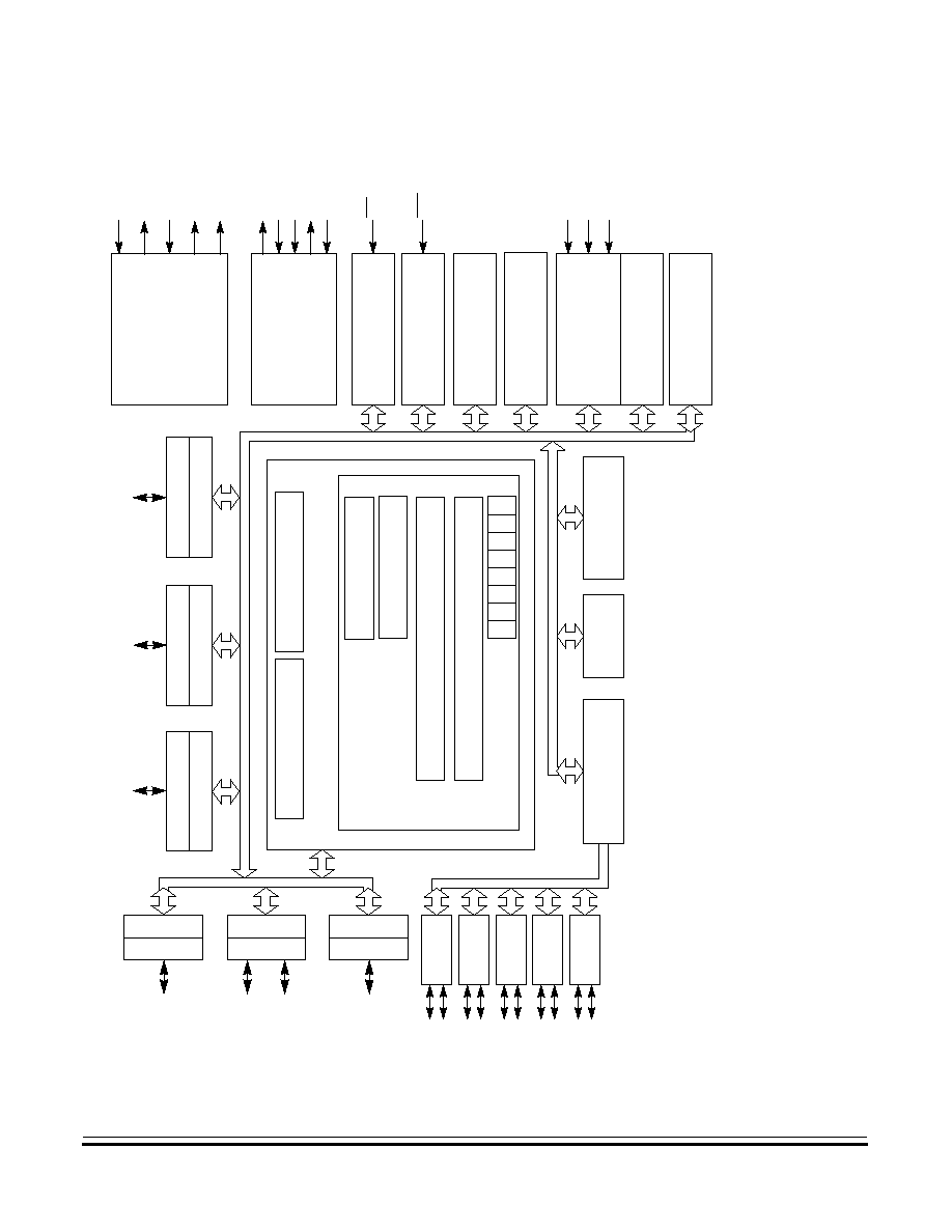
1.4 MCU Block Diagram
Figure 1-1
shows the structure of the MC68HC(7)08KH12.
MC68HC(7)08KH12
--
Re
v
.
1.0
Adv
ance Inf
or
mation
MOTOROLA
General Description
27
General Description
MCU Block Diagram
Figure 1-1. MCU Block Diagram
DS Port 1
PORTS ARE SOFTWARE CONFIGURABLE WITH PULLUP DEVICE IF INPUT PORT
SOFTWARE CONFIGURABLE LED DIRECT DRIVE 3mA SOURCE /10mA SINK or STANDARD DRIVE
PIN CONTAINS INTEGRATED PULLUP DEVICE
PIN HAS INTERRUPT CAPABILITY
PIN HAS INTERRUPT AND INTEGRATED PULLUP DEVICE.
PIN HAS OPTICAL COUPLING INTERFACE
OSC1
OSC2
RST
IRQ1/VPP
VDD1
VSS1
PTC4≠PTC0
REGOUT
PTB7≠PTB0
PTA7≠PTA0
PTE3/KBE3≠
PTE0/KBE0
VDD2
VSS2
VSSA
VDDA
CGMXFC
DPLUS4
TCH0/PTE1
TCH1/PTE2
TCLK/PTE0
PORT C
DDRC
PORT B
DDRB
PORT A
DDRA
POR
T D
DDRD
POR
T E
DDRE
POR
T F
DDRF
Embedded USB Function
384 bytes RAM
12k-bytes ROM/OTPROM
68HC08 CPU
CPU CONTROL
ALU
CPU REGISTERS
ACCUMULATOR
INDEX REGISTER
STACK POINTER
PROGRAM COUNTER
CONDITION CODE REGISTER
V 1 1 H
I
N Z C
DMINUS4
DPLUS3
DMINUS3
DPLUS2
DMINUS2
DPLUS1
DMINUS1
DPLUS0
US Port
DMINUS0
MONITOR ROM
240 bytes
COP MODULE
TIMER INTERFACE
MODULE
POWER-ON RESET
MODULE
BREAK MODULE
IRQ MODULE
SYSTEM INTEGRATION
MODULE
CLOCK GENERATION
MODULE AND PLL
POWER SUPPLY
AND
VOLTAGE REGULATION
PTD7/KBD7≠
PTD0/KBD0
DS Port 2
DS Port 3
DS Port 4
PTF7/KBF7≠
PTF0/KBF0
PTE4
General Description
Advance Information
MC68HC(7)08KH12
--
Rev. 1.0
28
General Description
MOTOROLA
1.5 Pin Assignments
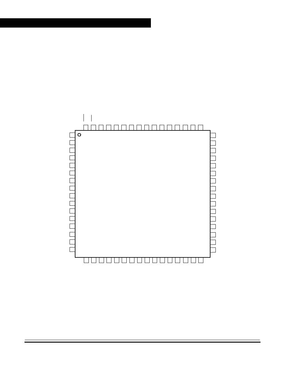
1.5.1 Quad Flat Pack (QFP) Package
Figure 1-2
Shows the 64-pin QFP assignments.
Figure 1-2. 64-Pin QFP Assignments (Top View)
DMINUS0
DPLUS0
REGOUT
VSSA
OSC2
OSC1
CGMXFC
VDDA
DPLUS1
DMINUS1
DPLUS2
DMINUS2
DPLUS3
1
2
3
4
5
6
7
8
9
10
11
12
13
DMINUS3
DPLUS4
DMINUS4
14
15
16
PTB4
PTB5
PTB6
PTB7
PTA0
PTA1
PTA2
PTA3
PTB3
PTB2
PTB1
PTB0
PTD7/KBD7
47
46
45
44
42
42
41
40
39
38
37
36
PTD6/KBD6
PTD5/KBD5
PTD4/KBD4
35
34
33
PTF5/KBF5
PTF4/KBF4
PTF3/KBF3
PTF2/KBF2
PTF1/KBF1
PTF0/KBF0
RST
IRQ1
/VPP
PTF6/KBF6
PTF7/KBF7
VSS2
VDD2
PTA7
63
62
61
60
59
58
57
56
55
54
53
52
PTA6
PTA5
PTA4
51
50
49
PTC0
VDD1
VSS1
PTE0/KBE0/TCLK
PTE1/KBE1/TCH0
PTE2/KBE2/TCH1
PTE3/KBE3
PTE4
PTC1
PTC2
PTC3
PTC4
PTD0/KBD0
18
19
20
21
22
23
24
25
26
27
28
29
PTD1/KBD1
PTD2/KBD2
PTD3/KBD3
30
31
32
64
17
48
68HC(7)08KH12
General Description
Pin Assignments
MC68HC(7)08KH12
--
Rev. 1.0
Advance Information
MOTOROLA
General Description
29
1.5.2 Power Supply Pins (V
DDA
, V
SSA
, V
DD1
, V
SS1
, V
DD2
, and V
SS2
)
V
DDA
and V
SSA
are the analog power supply and ground pins used by
the on-chip Phase-Locked Loop circuit.
V
DD2
and V
SS2
are the power supply and ground pins used by the
internal circuitry of the chip.
V
DD1
and V
SS1
are the power supply and ground pins to the I/O pads.
The MCU operates from a single power supply.
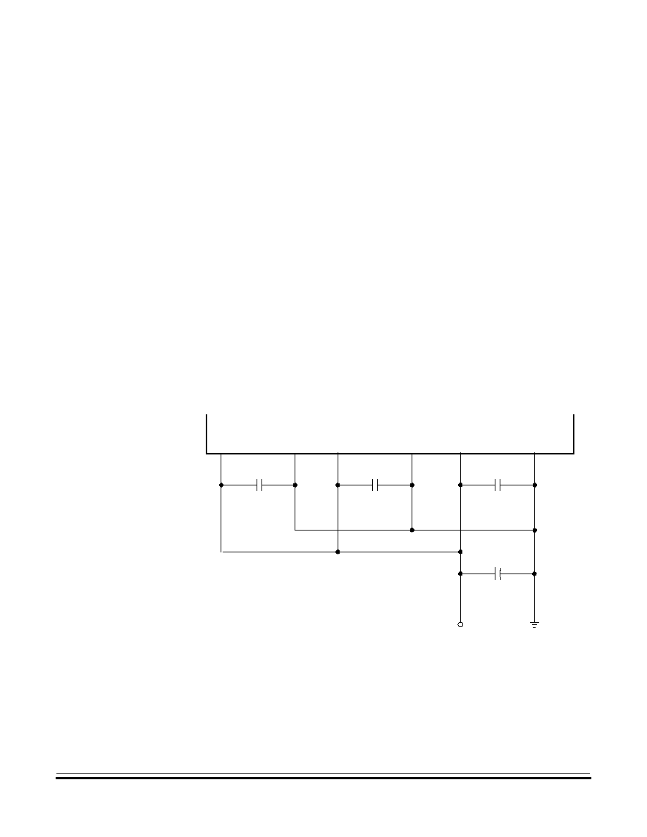
Fast signal transitions on MCU pins place high, short-duration current
demands on the power supply. To prevent noise problems, take special
care to provide power supply bypassing at the MCU as
Figure 1-3
shows. Place the bypass capacitors as close to the MCU power pins as
possible. Use high-frequency-response ceramic capacitors for C
BYPASS
.
C
BULK
are optional bulk current bypass capacitors for use in applications
that require the port pins to source high current levels.
Figure 1-3. Power Supply Bypassing
MCU
C
BULK
C
BYPASS
10nF
V
SS1
+
NOTE: Values shown are typical values.
V
DD2
C
BYPASS
10nF
V
DD2
C
BYPASS
10nF
V
SS2
V
SSA
V
DDA
Vbus

General Description
Advance Information
MC68HC(7)08KH12
--
Rev. 1.0
30
General Description
MOTOROLA
1.5.3 Oscillator Pins (OSC1 and OSC2)
The OSC1 and OSC2 pins are the connections for the on-chip oscillator
circuit.
(See Section 8. Clock Generator Module (CGM)
.)
1.5.4 External Reset Pin (RST)
A logic zero on the RST pin forces the MCU to a known start-up state.
RST is bidirectional, allowing a reset of the entire system. It is driven low
when any internal reset source is asserted. The RST pin contains an
internal pullup device. (
(See Section 7. System Integration Module
(SIM)
.)
1.5.5 External Interrupt Pin (IRQ1/V
PP
)
IRQ1/V
PP
is an asynchronous external interrupt pin. IRQ1/V
PP
is also
the OTPROM programming power pin. The IRQ1/V
PP
pin contain an
internal pullup device.
(See Section 14. External Interrupt (IRQ)
.)
1.5.6 USB Data Pins (DPLUS0≠DPLUS4 and DMINUS0≠DMINUS4)
DPLUS0≠DPLUS4 and DMINUS0≠DMINUS4 are the differential data
lines used by the USB module.
(See Section 9. Universal Serial Bus
Module (USB)
.)
1.5.7 Voltage Regulator Out (REGOUT)
REGOUT is the 3.3V output of the on-chip voltage regulator. It is used
to supply the voltage for the external pullup resistor required by the USB
on either DPLUS or DMINUS lines, depending on type of USB function.
REGOUT is also used internally for the USB data driver and the Phase-
locked Loop circuit. The REGOUT pin requires an external bulk
capacitor 1
µ
F or larger and a bypass capacitor.
(See Section 9.
Universal Serial Bus Module (USB)
.)

General Description
Pin Assignments
MC68HC(7)08KH12
--
Rev. 1.0
Advance Information
MOTOROLA
General Description
31
1.5.8 Port A Input/Output (I/O) Pins (PTA7≠PTA0)
PTA7≠PTA0 are general-purpose bidirectional I/O port pins.
(See
Section 12. I/O Ports
.) Each pin contains a software configurable pull-
up device when the pin is configured as an input.
(See 12.9 Port
Options
.)
1.5.9 Port B I/O Pins (PTB7≠PTB0)
PTB7≠PTB0 are general-purpose bidirectional I/O port pins.
(See
Section 12. I/O Ports
.) Each pin contains a software configurable pull-
up device when the pin is configured as an input.
(See 12.9 Port
Options
.)
1.5.10 Port C I/O Pins (PTC4≠PTC0)
PTC4≠PTC0 are general-purpose bidirectional I/O port pins.
(See
Section 12. I/O Ports
.) Port C pins are software configurable to be LED
Direct Drive ports. Each pin contains a software configurable pull-up
device when the pin is configured as an input.
(See 12.9 Port Options
.)
1.5.11 Port D I/O Pins (PTD7/KBD7≠PTD0/KBD0)
PTD7/KBD7≠PTD0/KBD0 are general-purpose bidirectional I/O port
pins.
(See Section 12. I/O Ports
.) Any or all of the port D pins can be
programmed to serve as external interrupt pins.
(See Section 15.
Keyboard Interrupt Module (KBI)
.)
1.5.12 Port E I/O Pins (PTE4, PTE3/KBE3, PTE2/KBE2/TCH1,
PTE1/KBE1/TCH0, PTE0/KBE0/TCLK)
Port-E is a 5-bit special function port which shares three of its pins with
the Timer Interface Module and four of its pins with Keyboard Interrupt
Module (
see Section 12. I/O Ports
,
Section 15. Keyboard Interrupt
Module (KBI)
and
Section 11. Timer Interface Module (TIM)
). In
addition, PTE3-PTE0 has built-in optical coupling interface for optical
mouse application.
(See Section 12. I/O Ports
.)

General Description
Advance Information
MC68HC(7)08KH12
--
Rev. 1.0
32
General Description
MOTOROLA
1.5.13 Port F I/O Pins (PTF7/KBF7≠PTF0/KBF0)
PTF7/KBF7≠PTF0/KBF0 are general-purpose bidirectional I/O port pins.
(See Section 12. I/O Ports
.) Any or all of the port F pins can be
programmed to serve as external interrupt pins.
(See Section 15.
Keyboard Interrupt Module (KBI)
.)

MC68HC(7)08KH12
--
Rev. 1.0
Advance Information
MOTOROLA
Memory Map
33
Advance Information -- MC68HC(7)08KH12
Section 2. Memory Map
2.1 Contents
2.2
Introduction . . . . . . . . . . . . . . . . . . . . . . . . . . . . . . . . . . . . . . . . 33
2.3
I/O Section . . . . . . . . . . . . . . . . . . . . . . . . . . . . . . . . . . . . . . . . 35
2.4
Monitor ROM . . . . . . . . . . . . . . . . . . . . . . . . . . . . . . . . . . . . . . 43
2.2 Introduction
The CPU08 can address 64 Kbytes of memory space. The memory
map, shown in
Figure 2-1
, includes:
∑
11776 bytes of ROM or OTPROM
∑
384 bytes of RAM
∑
26 bytes of user-defined vectors
∑
240 bytes of Monitor ROM
Memory Map
Advance Information
MC68HC(7)08KH12
--
Rev. 1.0
34
Memory Map
MOTOROLA
$0000
$005F
I/O REGISTERS (80 BYTES)
$0060
$01DF
RAM (384 BYTES)
$01E0
$CDFF
UNIMPLEMENTED (52, 256 BYTES)
$D000
$FDFF
ROM/OTPROM (11776 BYTES)
$FE00
BREAK STATUS REGISTER (BSR)
$FE01
RESET STATUS REGISTER (RSR)
$FE02
RESERVED
$FE03
BREAK FLAG CONTROL REGISTER (BFCR)
$FE04
INTERRUPT STATUS REGISTER 1 (INT1)
$FE05
INTERRUPT STATUS REGISTER 2 (INT2)
$FE06
RESERVED
$FE07
RESERVED
$FE08
$FE0B
RESERVED (4 BYTES)
$FE0C
BREAK ADDRESS HIGH REGISTER (BRKH)
$FE0D
BREAK ADDRESS LOW REGISTER (BRKL)
$FE0E
BREAK STATUS AND CONTROL REGISTER (BSCR)
$FE0F
RESERVED
$FE10
$FEFF
MONITOR ROM (240 BYTES)
$FF00
$FF00 to $FF8C
UNIMPLEMENTED (141 BYTES)
$FF8D
RESERVED
$FFE5
$FF8E to $FFE5
UNIMPLEMENTED (88 BYTES)
$FFE6
$FFFF
VECTORS (26 BYTES)
Figure 2-1. Memory Map

Memory Map
I/O Section
MC68HC(7)08KH12
--
Rev. 1.0
Advance Information
MOTOROLA
Memory Map
35
2.3 I/O Section
Addresses $0000≠$005F, shown in
Figure 2-2
, contain most of the
control, status, and data registers. Additional I/O registers have the
following addresses:
∑
$FE00 (Break Status Register, BSR)
∑
$FE01 (Reset Status Register, RSR)
∑
$FE02 (Reserved)
∑
$FE03 (Break Flag Control Register, BFCR)
∑
$FE04 (Interrupt Status Register 1, INT1)
∑
$FE05 (Interrupt Status Register 2, INT2)
∑
$FE06 (Reserved)
∑
$FE07 (Reserved)
∑
$FE08 (Reserved)
∑
$FE09 (Reserved)
∑
$FE0A (Reserved)
∑
$FE0B (Reserved)
∑
$FE0C and $FE0D (Break Address Registers, BRKH and BRKL)
∑
$FE0E (Break Status and Control Register, BSCR)
∑
$FF8D (Reserved)
∑
$FFFF (COP Control Register, COPCTL)
Memory Map
Advance Information
MC68HC(7)08KH12
--
Rev. 1.0
36
Memory Map
MOTOROLA
Addr.
Name
Bit 7
6
5
4
3
2
1
Bit 0
$0000
Port A Data Register (PTA)
R:
PTA7
PTA6
PTA5
PTA4
PTA3
PTA2
PTA1
PTA0
W:
$0001
Port B Data Register (PTB)
R:
PTB7
PTB6
PTB5
PTB4
PTB3
PTB2
PTB1
PTB0
W:
$0002
Port C Data Register (PTC)
R:
0
0
0
PTC4
PTC3
PTC2
PTC1
PTC0
W:
$0003
Port D Data Register (PTD)
R:
PTD7
PTD6
PTD5
PTD4
PTD3
PTD2
PTD1
PTD0
W:
$0004
Data Direction Register A (DDRA)
R:
DDRA7
DDRA6
DDRA5
DDRA4
DDRA3
DDRA2
DDRA1
DDRA0
W:
$0005
Data Direction Register B (DDRB)
R:
DDRB7
DDRB6
DDRB5
DDRB4
DDRB3
DDRB2
DDRB1
DDRB0
W:
$0006
Data Direction Register C (DDRC)
R:
0
0
0
DDRC4
DDRC3
DDRC2
DDRC1
DDRC0
W:
$0007
Data Direction Register D (DDRD)
R:
DDRD7
DDRD6
DDRD5
DDRD4
DDRD3
DDRD2
DDRD1
DDRD0
W:
$0008
Port E Data Register (PTE)
R:
0
0
0
PTE4
PTE3
PTE2
PTE1
PTE0
W:
$0009
Port F Data Register (PTF)
R:
PTF7
PTF6
PTF5
PTF4
PTF3
PTF2
PTF1
PTF0
W:
$000A
Data Direction Register E (DDRE)
R:
0
0
0
DDRE4
DDRE3
DDRE2
DDRE1
DDRE0
W:
$000B
Data Direction Register F (DDRF)
R:
DDRF7
DDRF6
DDRF5
DDRF4
DDRF3
DDRF2
DDRF1
DDRF0
W:
$000C
Port D Keyboard Status and
Control Register (KBDSCR)
R:
0
0
0
0
KEYDF
0
IMASKD
MODED
W:
ACKD
$000D
Port D Keyboard Interrupt Enable
Register (KBDIER)
R: KBDIE7
KBDIE6
KBDIE5
KBDIE4
KBDIE3
KBDIE2
KBDIE1
KBDIE0
$000E
Port E Keyboard Status and
Control Register (KBESCR)
R:
0
0
0
0
KEYEF
0
IMASKE
MODEE
W:
ACKE
$000F
Port E Keyboard Interrupt Enable
Register (KBEIER)
R:
PEPE3
PEPE2
PEPE1
PEPE0
KBEIE3
KBEIE2
KBEIE1
KBEIE0
W:
= Unimplemented
R
= Reserved
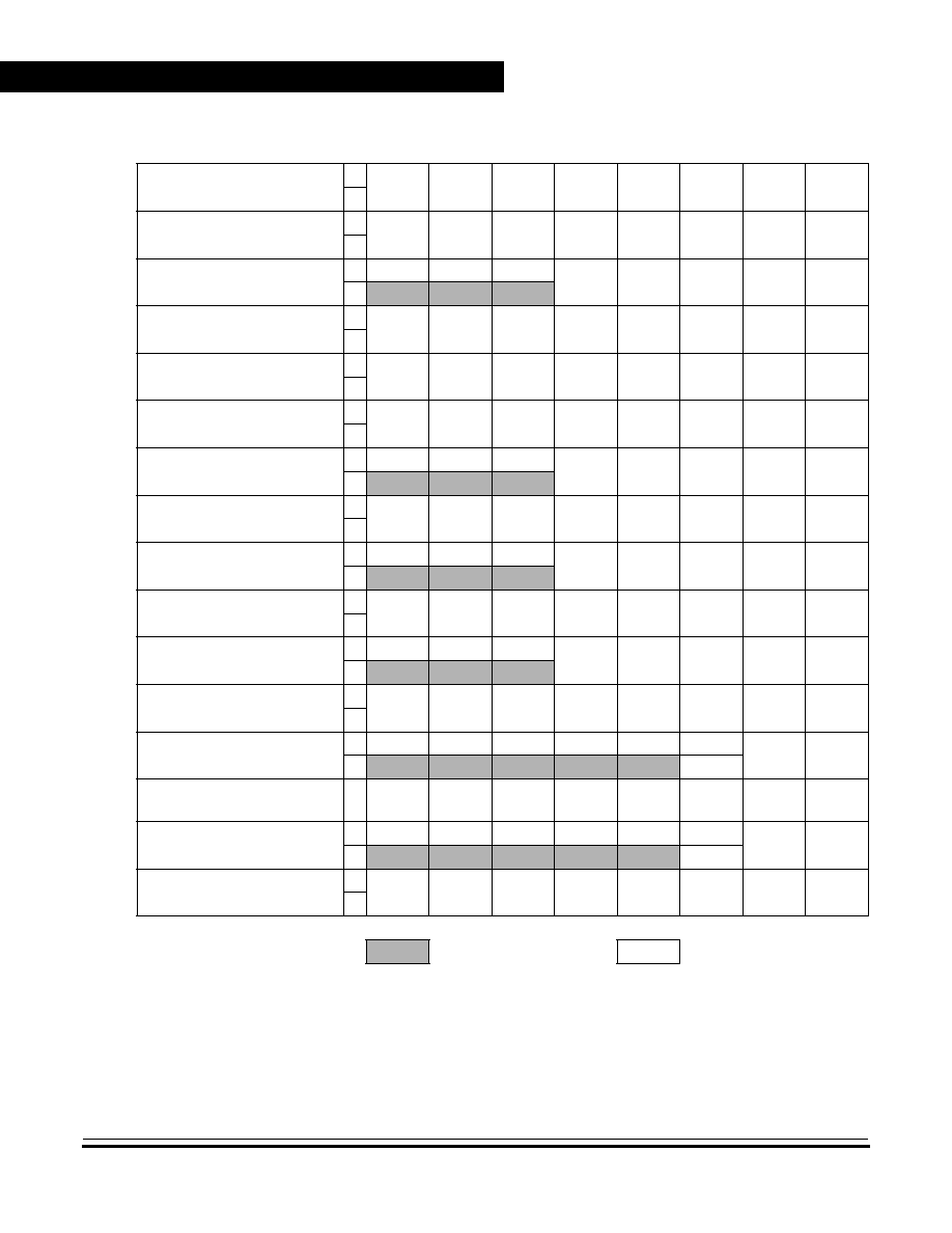
Figure 2-2. Control, Status, and Data Registers
Memory Map
I/O Section
MC68HC(7)08KH12
--
Rev. 1.0
Advance Information
MOTOROLA
Memory Map
37
$0010
TIM Status and Control Register
(TSC)
R:
TOF
TOIE
TSTOP
0
0
PS2
PS1
PS0
W:
0
TRST
$0011
Unimplemented
R:
W:
$0012
TIM Counter Register High
(TCNTH)
R:
Bit 15
14
13
12
11
10
9
Bit 8
W:
$0013
TIM Counter Register Low
(TCNTL)
R:
Bit 7
6
5
4
3
2
1
Bit 0
W:
$0014
TIM Counter Modulo Register High
(TMODH)
R:
Bit 15
14
13
12
11
10
9
Bit 8
W:
$0015
TIM Counter Modulo Register Low
(TMODL)
R:
Bit 7
6
5
4
3
2
1
Bit 0
W:
$0016
TIM Channel 0 Status and Control
Register (TSC0)
R:
CH0F
CH0IE
MS0B
MS0A
ELS0B
ELS0A
TOV0
CH0MAX
W:
0
$0017
TIM Channel 0 Register High
(TCH0H)
R:
Bit 15
14
13
12
11
10
9
Bit 8
W:
$0018
TIM Channel 0 Register Low
(TCH0L)
R:
Bit 7
6
5
4
3
2
1
Bit 0
W:
$0019
TIM Channel 1 Status and Control
Register (TSC1)
R:
CH1F
CH1IE
0
MS1A
ELS1B
ELS1A
TOV1
CH1MAX
W:
0
$001A
TIM Channel 1 Register High
(TCH1H)
R:
Bit 15
14
13
12
11
10
9
Bit 8
$001B
TIM Channel 1 Register Low
(TCH1L)
R:
Bit 7
6
5
4
3
2
1
Bit 0
W:
$001C
PORT E Optical Interface Enable
Register (EOIER)
R:
YREF2
YREF1
YREF0
XREF2
XREF1
XREF0
OIEY
OIEX
W:
$001D Port Option Control Register (POC)
R:
0
0
LDD
0
0
PCP
PBP
PAP
W:
$001E
IRQ Status and Control Register
(ISCR)
R:
0
0
0
0
IRQF1
0
IMASK1
MODE1
W
ACK1
$001F
Configuration Register
(CONFIG)
R:
0
0
0
0
SSREC
COPRS
STOP
COPD
W:
One-time writable register
Addr.
Name
Bit 7
6
5
4
3
2
1
Bit 0
= Unimplemented
R
= Reserved
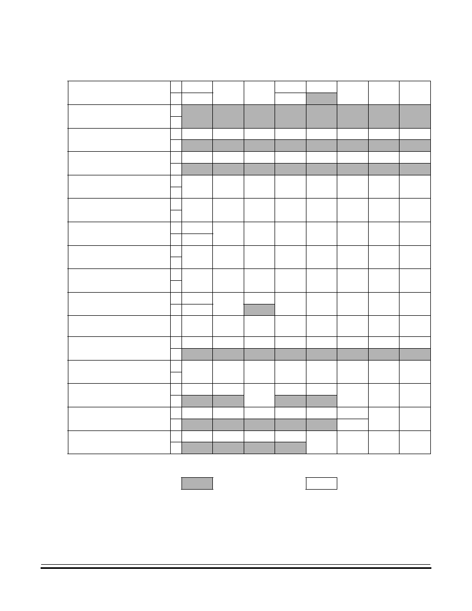
Figure 2-2. Control, Status, and Data Registers (Continued)
Memory Map
Advance Information
MC68HC(7)08KH12
--
Rev. 1.0
38
Memory Map
MOTOROLA
$0020
USB Embedded Device Endpoint 0
Data Register 0 (DE0D0)
R: DE0R07
DE0R06
DE0R05
DE0R04
DE0R03
DE0R02
DE0R01
DE0R00
W: DE0T07
DE0T06
DE0T05
DE0T04
DE0T03
DE0T02
DE0T01
DE0T00
$0021
USB Embedded Device Endpoint 0
Data Register 1 (DE0D1)
R: DE0R17
DE0R16
DE0R15
DE0R14
DE0R13
DE0R12
DE0R11
DE0R10
W: DE0T17
DE0T16
DE0T15
DE0T14
DE0T13
DE0T12
DE0T11
DE0T10
$0022
USB Embedded Device Endpoint 0
Data Register 2 (DE0D2)
R: DE0R27
DE0R26
DE0R25
DE0R24
DE0R23
DE0R22
DE0R21
DE0R20
W: DE0T27
DE0T26
DE0T25
DE0T24
DE0T23
DE0T22
DE0T21
DE0T20
$0023
USB Embedded Device Endpoint 0
Data Register 3 (DE0D3)
R: DE0R37
DE0R36
DE0R35
DE0R34
DE0R33
DE0R32
DE0R31
DE0R30
W: DE0T37
DE0T36
DE0T35
DE0T34
DE0T33
DE0T32
DE0T31
DE0T30
$0024
USB Embedded Device Endpoint 0
Data Register 4 (DE0D4)
R: DE0R47
DE0R46
DE0R45
DE0R44
DE0R43
DE0R42
DE0R41
DE0R40
W: DE0T47
DE0T46
DE0T45
DE0T44
DE0T43
DE0T42
DE0T41
DE0T40
$0025
USB Embedded Device Endpoint 0
Data Register 5 (DE0D5)
R: DE0R57
DE0R56
DE0R55
DE0R54
DE0R53
DE0R52
DE0R51
DE0R50
W: DE0T57
DE0T56
DE0T55
DE0T54
DE0T53
DE0T52
DE0T51
DE0T50
$0026
USB Embedded Device Endpoint 0
Data Register 6 (DE0D6)
R: DE0R67
DE0R66
DE0R65
DE0R64
DE0R63
DE0R62
DE0R61
DE0R60
W: DE0T67
DE0T66
DE0T65
DE0T64
DE0T63
DE0T62
DE0T61
DE0T60
$0027
USB Embedded Device Endpoint 0
Data Register 7 (DE0D7)
R: DE0R77
DE0R76
DE0R75
DE0R74
DE0R73
DE0R72
DE0R71
DE0R70
W: DE0T77
DE0T76
DE0T75
DE0T74
DE0T73
DE0T72
DE0T71
DE0T70
$0028
USB Embedded Device Endpoint
1/2 Data Register 0 (DE1D0)
R:
W: DE1T07
DE1T06
DE1T05
DE1T04
DE1T03
DE1T02
DE1T01
DE1T00
$0029
USB Embedded Device Endpoint
1/2 Data Register 1 (DE1D1)
R:
W: DE1T17
DE1T16
DE1T15
DE1T14
DE1T13
DE1T12
DE1T11
DE1T10
$002A
USB Embedded Device Endpoint
1/2 Data Register 2 (DE1D2)
R:
W: DE1T27
DE1T26
DE1T25
DE1T24
DE1T23
DE1T22
DE1T21
DE1T20
$002B
USB Embedded Device Endpoint
1/2 Data Register 3 (DE1D3)
R:
W: DE1T37
DE1T36
DE1T35
DE1T34
DE1T33
DE1T32
DE1T31
DE1T30
$002C
USB Embedded Device Endpoint
1/2 Data Register 4 (DE1D4)
R:
W: DE1T47
DE1T46
DE1T45
DE1T44
DE1T43
DE1T42
DE1T41
DE1T40
$002D
USB Embedded Device Endpoint
1/2 Data Register 5 (DE1D5)
R:
W: DE1T57
DE1T56
DE1T55
DE1T54
DE1T53
DE1T52
DE1T51
DE1T50
$002E
USB Embedded Device Endpoint
1/2 Data Register 6 (DE1D6)
R:
W: DE1T67
DE1T66
DE1T65
DE1T64
DE1T63
DE1T62
DE1T61
DE1T60
$002F
USB Embedded Device Endpoint
1/2 Data Register 7 (DE1D7)
R:
W: DE1T77
DE1T76
DE1T75
DE1T74
DE1T73
DE1T72
DE1T71
DE1T70
Addr.
Name
Bit 7
6
5
4
3
2
1
Bit 0
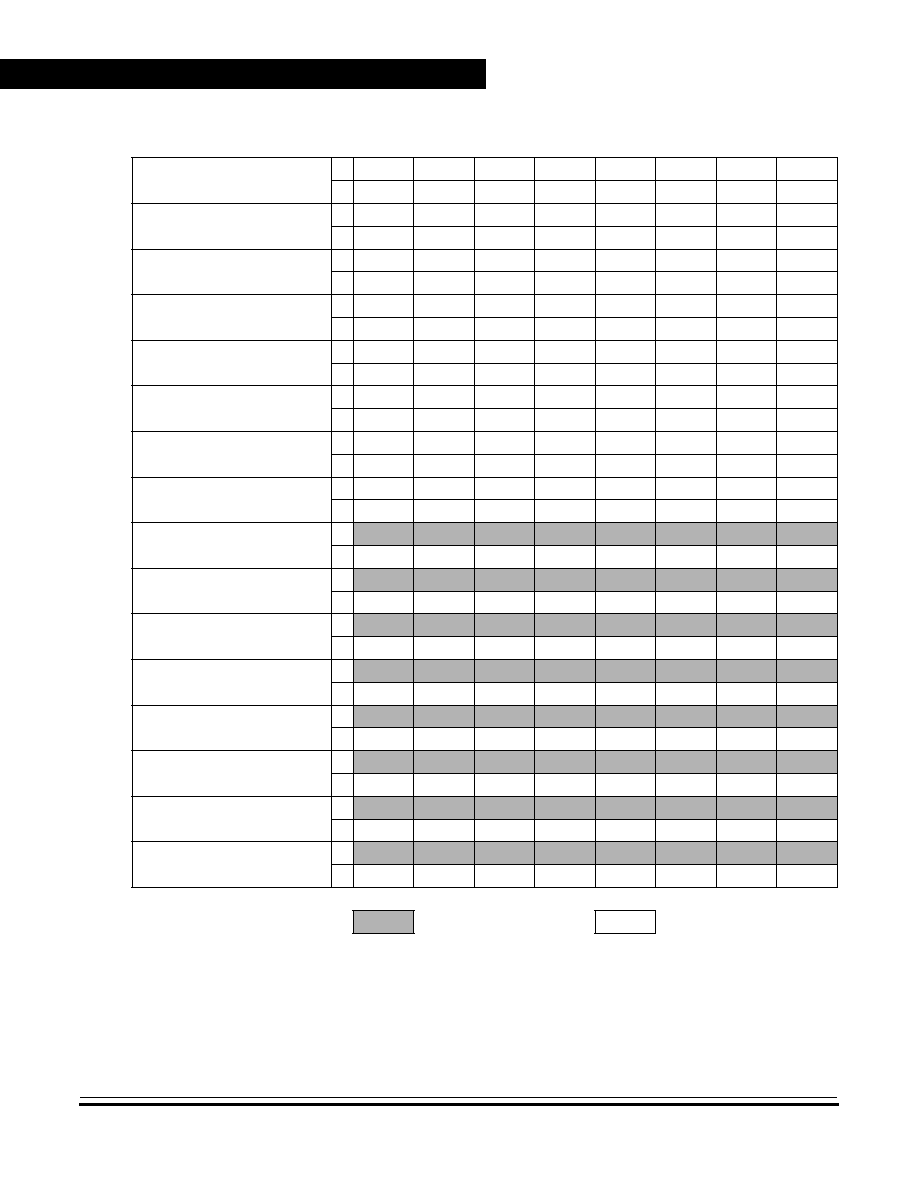
= Unimplemented
R
= Reserved
Figure 2-2. Control, Status, and Data Registers (Continued)
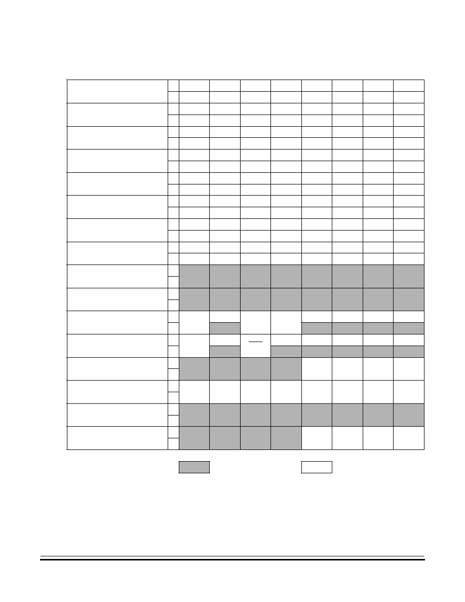
Memory Map
I/O Section
MC68HC(7)08KH12
--
Rev. 1.0
Advance Information
MOTOROLA
Memory Map
39
$0030
USB HUB Endpoint 0 Data
Register 0 (HE0D0)
R: HE0R07
HE0R06
HE0R05
HE0R04
HE0R03
HE0R02
HE0R01
HE0R00
W: HE0T07
HE0T06
HE0T05
HE0T04
HE0T03
HE0T02
HE0T01
HE0T00
$0031
USB HUB Endpoint 0 Data
Register 1 (HE0D1)
R: HE0R17
HE0R16
HE0R15
HE0R14
HE0R13
HE0R12
HE0R11
HE0R10
W: HE0T17
HE0T16
HE0T15
HE0T14
HE0T13
HE0T12
HE0T11
HE0T10
$0032
USB HUB Endpoint 0 Data
Register 2 (HE0D2)
R: HE0R27
HE0R26
HE0R25
HE0R24
HE0R23
HE0R22
HE0R21
HE0R20
W: HE0T27
HE0T26
HE0T25
HE0T24
HE0T23
HE0T22
HE0T21
HE0T20
$0033
USB HUB Endpoint 0 Data
Register 3 (HE0D3)
R: HE0R37
HE0R36
HE0R35
HE0R34
HE0R33
HE0R32
HE0R31
HE0R30
W: HE0T37
HE0T36
HE0T35
HE0T34
HE0T33
HE0T32
HE0T31
HE0T30
$0034
USB HUB Endpoint 0 Data
Register 4 (HE0D4)
R: HE0R47
HE0R46
HE0R45
HE0R44
HE0R43
HE0R42
HE0R41
HE0R40
W: HE0T47
HE0T46
HE0T45
HE0T44
HE0T43
HE0T42
HE0T41
HE0T40
$0035
USB HUB Endpoint 0 Data
Register 5 (HE0D5)
R: HE0R57
HE0R56
HE0R55
HE0R54
HE0R53
HE0R52
HE0R51
HE0R50
W: HE0T57
HE0T56
HE0T55
HE0T54
HE0T53
HE0T52
HE0T51
HE0T50
$0036
USB HUB Endpoint 0 Data
Register 6 (HE0D6)
R: HE0R67
HE0R66
HE0R65
HE0R64
HE0R63
HE0R62
HE0R61
HE0R60
W: HE0T67
HE0T66
HE0T65
HE0T64
HE0T63
HE0T62
HE0T61
HE0T60
$0037
USB HUB Endpoint 0 Data
Register 7 (HE0D7)
R: HE0R77
HE0R76
HE0R75
HE0R74
HE0R73
HE0R72
HE0R71
HE0R70
W: HE0T77
HE0T76
HE0T75
HE0T74
HE0T73
HE0T72
HE0T71
HE0T70
$0038
Unimplemented
R:
W:
$0039
Unimplemented
R:
W:
$003A
PLL Control Register
(PCTL)
R:
PLLIE
PLLF
PLLON
BCS
PRE1
PRE0
0
0
W:
$003B
PLL Bandwidth Control Register
(PBWC)
R:
AUTO
LOCK
ACQ
0
0
0
0
0
W:
$003C
PLL Multiplier Select Register High
(PMSH)
R:
MUL11
MUL10
MUL9
MUL8
W:
$003D
PLL Multiplier Select Register Low
(PMSL)
R:
MUL7
MUL6
MUL5
MUL4
MUL3
MUL2
MUL1
MUL0
W:
$003E
Unimplemented
R:
W:
$003F
PLL Reference Divider Select
Register (PRDS)
R:
RDS3
RDS2
RDS1
RDS0
W:
Addr.
Name
Bit 7
6
5
4
3
2
1
Bit 0
= Unimplemented
R
= Reserved
Figure 2-2. Control, Status, and Data Registers (Continued)
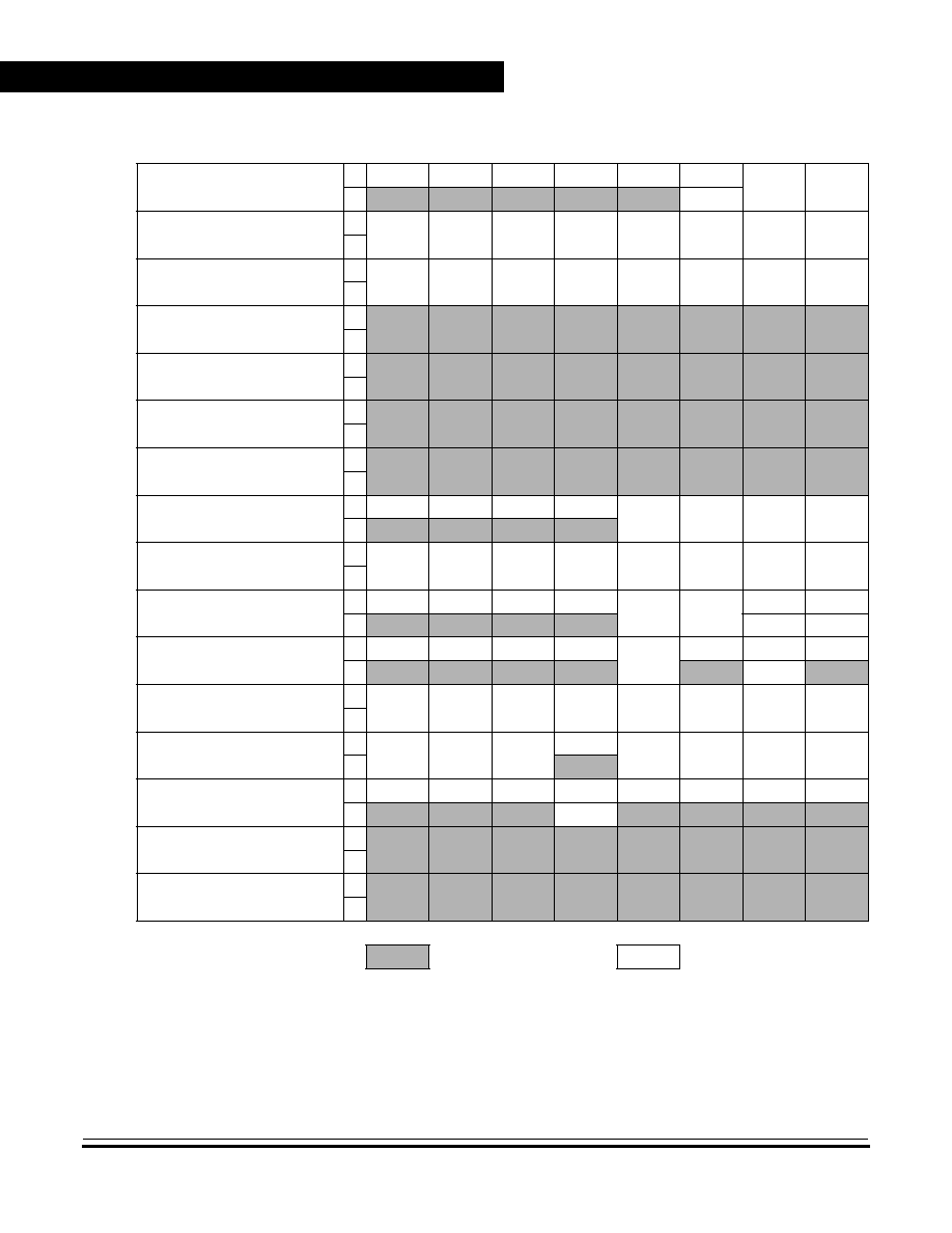
Memory Map
Advance Information
MC68HC(7)08KH12
--
Rev. 1.0
40
Memory Map
MOTOROLA
$0040
Port F Keyboard Status and Control
Register (KBFSCR)
R:
0
0
0
0
KEYFF
0
IMASKF
MODEF
W:
ACKF
$0041
Port F Keyboard Interrupt Enable
Register (KBFIER)
R:
KBFIE7
KBFIE6
KBFIE5
KBFIE4
KBFIE3
KBFIE2
KBFIE1
KBFIE0
W:
$0042
Port F Pull-up Enable Register
(PFPER)
R:
PFPE7
PFPE6
PFPE5
PFPE4
PFPE3
PFPE2
PFPE1
PFPE0
W:
$0043
Unimplemented
R:
W:
$0044
Unimplemented
R:
W:
$0045
Unimplemented
R:
W:
$0046
Unimplemented
R:
W:
$0047
USB Embedded Device Control
Register 2 (DCR2)
R:
0
0
0
0
ENABLE2 ENABLE1 DSTALL2
DSTALL1
W:
$0048
USB Embedded Device Address
Register (DADDR)
R:
DEVEN
DADD6
DADD5
DADD4
DADD3
DADD2
DADD1
DADD0
W:
$0049
USB Embedded Device Interrupt
Register 0 (DIR0)
R: TXD0F
RXD0F
0
0
TXD0IE
RXD0IE
0
0
W:
TXD0FR RXD0FR
$004A
USB Embedded Device Interrupt
Register 1 (DIR1)
R: TXD1F
0
0
0
TXD1IE
0
0
0
W:
TXD1FR
$004B
USB Embedded Device Control
Register 0 (DCR0)
R:
T0SEQ
DSTALL0
TX0E
RX0E
TP0SIZ3 TP0SIZ2 TP0SIZ1 TP0SIZ0
W:
$004C
USB Embedded Device Control
Register 1 (DCR1)
R:
T1SEQ
ENDADD
TX1E
0
TP1SIZ3 TP1SIZ2 TP1SIZ1 TP1SIZ0
W:
$004D
USB Embedded Device Status
Register (DSR)
R: DRSEQ DSETUP DTX1ST
0
RP0SIZ3 RP0SIZ2 RP0SIZ1 RP0SIZ0
W:
DTX1STR
$004E
Unimplemented
R:
W:
$004F
Unimplemented
R:
W:
Addr.
Name
Bit 7
6
5
4
3
2
1
Bit 0
= Unimplemented
R
= Reserved
Figure 2-2. Control, Status, and Data Registers (Continued)
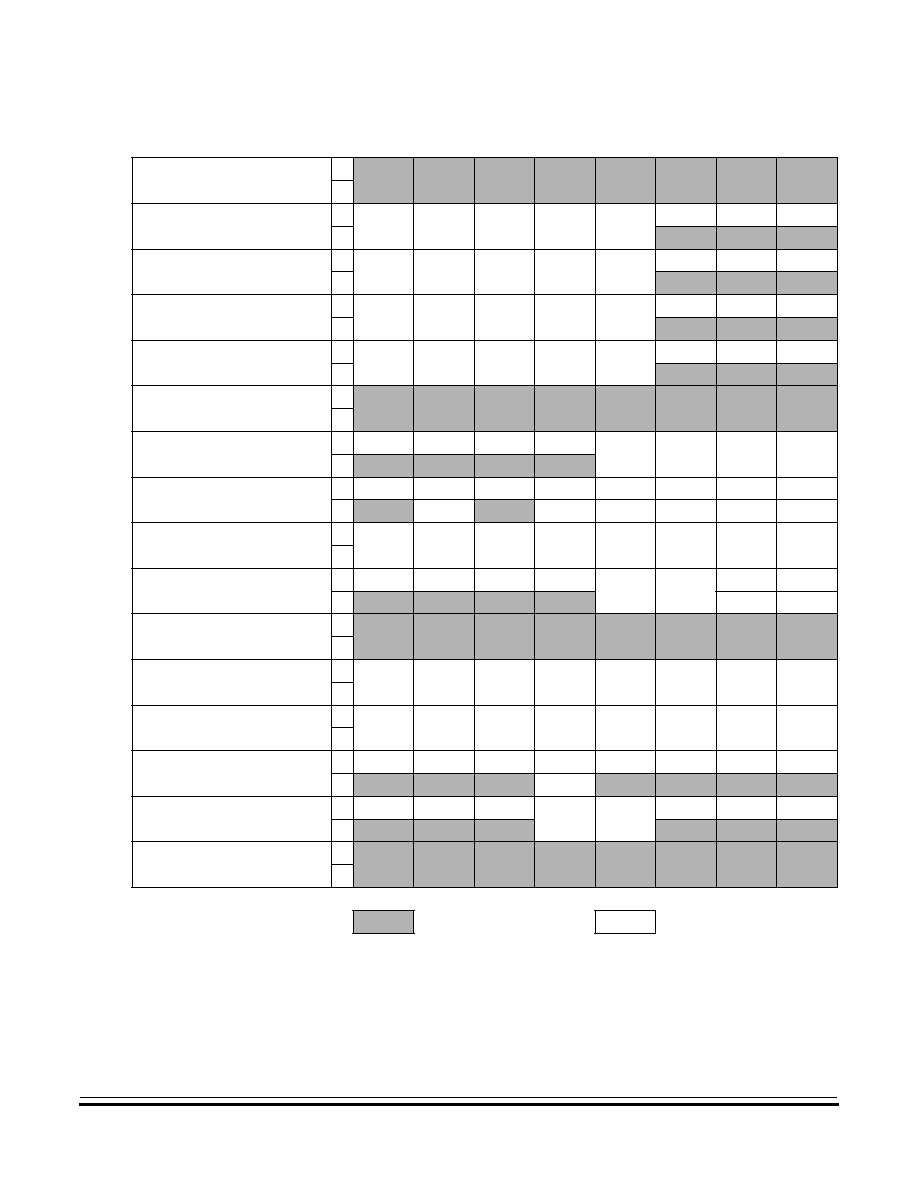
Memory Map
I/O Section
MC68HC(7)08KH12
--
Rev. 1.0
Advance Information
MOTOROLA
Memory Map
41
$0050
Unimplemented
R:
W:
$0051
USB HUB Downstream Port 1
Control Register (HDP1CR)
R:
PEN1
LOWSP1
RST1
RESUM1
SUSP1
0
D1+
D1≠
W:
$0052
USB HUB Downstream Port 2
Control Register (HDP2CR)
R:
PEN2
LOWSP2
RST2
RESUM2
SUSP2
0
D2+
D2≠
W:
$0053
USB HUB Downstream Port 3
Control Register (HDP3CR)
R:
PEN3
LOWSP3
RST3
RESUM3
SUSP3
0
D3+
D3≠
W:
$0054
USB HUB Downstream Port 4
Control Register (HDP4CR)
R:
PEN4
LOWSP4
RST4
RESUM4
SUSP4
0
D4+
D4≠
W:
$0055
Unimplemented
R:
W:
$0056
USB SIE Timing Interrupt Register
(SIETIR)
R:
SOFF
EOF2F
EOPF
TRANF
SOFIE
EOF2IE
EOPIE
TRANIE
W:
$0057
USB SIE Timing Status Register
(SIETSR)
R:
RSTF
0
LOCKF
0
0
0
0
0
W:
RSTFR
LOCKFR
SOFFR
EOF2FR
EOPFR
TRANFR
$0058
USB HUB Address Register
(HADDR)
R:
USBEN
ADD6
ADD5
ADD4
ADD3
ADD2
ADD1
ADD0
W:
$0059
USB HUB Interrupt Register 0
(HIR0)
R:
TXDF
RXDF
0
0
TXDIE
RXDIE
0
0
W:
TXDFR
RXDFR
$005A
Unimplemented
R:
W:
$005B
USB HUB Control Register 0
(HCR0)
R:
TSEQ
STALL0
TXE
RXE
TPSIZ3
TPSIZ2
TPSIZ1
TPSIZ0
W:
$005C
USB HUB Endpoint1 Control &
Data Register (HCDR)
R:
STALL1
PNEW
PCHG5
PCHG4
PCHG3
PCHG2
PCHG1
PCHG0
W:
$005D
USB HUB Status Register (HSR)
R:
RSEQ
SETUP
TX1ST
0
RPSIZ3
RPSIZ2
RPSIZ1
RPSIZ0
W:
TX1STR
$005E
USB HUB Root Port Control
Register (HRPCR)
R:
0
0
0
RESUM0 SUSPND
0
D0+
D0≠
W:
$005F
Unimplemented
R:
W:
Addr.
Name
Bit 7
6
5
4
3
2
1
Bit 0
= Unimplemented
R
= Reserved
Figure 2-2. Control, Status, and Data Registers (Continued)
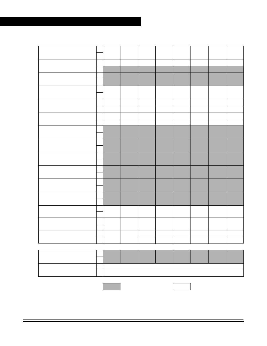
Memory Map
Advance Information
MC68HC(7)08KH12
--
Rev. 1.0
42
Memory Map
MOTOROLA
$FE00
Break Status Register
(BSR)
R:
R
R
R
R
R
R
SBSW
R
W:
$FE01
Reset Status Register
(RSR)
R:
POR
PIN
COP
ILOP
ILAD
USB
0
0
W:
$FE02
Reserved
R:
W:
$FE03
Break Flag Control Register
(BFCR)
R:
BCFE
R
R
R
R
R
R
R
W:
$FE04
Interrupt Status Register 1 (INT1)
R:
IF6
IF5
IF4
IF3
IF2
IF1
0
0
W:
R
R
R
R
R
R
R
R
$FE05
Interrupt Status Register 2 (INT2)
R:
0
0
0
IF11
IF10
IF9
IF8
IF7
W:
R
R
R
R
R
R
R
R
$FE06
Reserved
R:
W:
$FE07
Reserved
R:
W:
$FE08
Unimplemented
R:
W:
$FE09
Unimplemented
R:
W:
$FE0A
Unimplemented
R:
W:
$FE0B
Unimplemented
R:
W:
$FE0C
Break Address Register High
(BRKH)
R:
Bit 15
14
13
12
11
10
9
Bit 8
W:
$FE0D
Break Address Register Low
(BRKL)
R:
Bit 7
6
5
4
3
2
1
Bit 0
W:
$FE0E
Break Status and Control Register
(BRKSCR)
R:
BRKE
BRKA
0
0
0
0
0
0
W:
$FF8D
Reserved
R:
W:
$FFFF
COP Control Register
(COPCTL)
R:
Low byte of reset vector
W:
Writing clears COP counter (any value)
Addr.
Name
Bit 7
6
5
4
3
2
1
Bit 0
= Unimplemented
R
= Reserved
Figure 2-2. Control, Status, and Data Registers (Continued)
Memory Map
Monitor ROM
MC68HC(7)08KH12
--
Rev. 1.0
Advance Information
MOTOROLA
Memory Map
43
Table 2-1
is a list of vector locations.
2.4 Monitor ROM
The 240 bytes at addresses $FE10≠$FEFF are reserved ROM
addresses that contain the instructions for the monitor functions.
(See
Section 10. Monitor ROM (MON)
.)
Table 2-1. Vector Addresses
Address
Vector
$FFE6
PLL Vector (High)
$FFE7
PLL Vector (Low)
$FFE8
Port-F Keyboard Vector (High)
$FFE9
Port-F Keyboard Vector (Low)
$FFEA
Port-D Keyboard Vector (High)
$FFEB
Port-D Keyboard Vector (Low)
$FFEC
Port-E Keyboard Vector (High)
$FFED
Port-E Keyboard Vector (Low)
$FFEE
TIM Overflow Vector (High)
$FFEF
TIM Overflow Vector (Low)
$FFF0
TIM Channel 1 Vector (High)
$FFF1
TIM Channel 1 Vector (Low)
$FFF2
TIM Channel 0 Vector (High)
$FFF3
TIM Channel 0 Vector (Low)
$FFF4
USB Device Endpoint Interrupt Vector (High)
$FFF5
USB Device Endpoint Interrupt Vector (Low)
$FFF6
USB HUB Endpoint Interrupt Vector (High)
$FFF7
USB HUB Endpoint Interrupt Vector (Low)
$FFF8
USB SIE Timing Interrupt Vector (High)
$FFF9
USB SIE Timing Interrupt Vector (Low)
$FFFA
IRQ1 Vector (High)
$FFFB
IRQ1 Vector (Low)
$FFFC
SWI Vector (High)
$FFFD
SWI Vector (Low)
$FFFE
Reset Vector (High)
$FFFF
Reset Vector (Low)
Priority
Lo
w
High

Memory Map
Advance Information
MC68HC(7)08KH12
--
Rev. 1.0
44
Memory Map
MOTOROLA

MC68HC(7)08KH12
--
Rev. 1.0
Advance Information
MOTOROLA
Random-Access Memory (RAM)
45
Advance Information -- MC68HC(7)08KH12
Section 3. Random-Access Memory (RAM)
3.1 Contents
3.2
Introduction . . . . . . . . . . . . . . . . . . . . . . . . . . . . . . . . . . . . . . . . 45
3.3
Functional Description . . . . . . . . . . . . . . . . . . . . . . . . . . . . . . . 45
3.2 Introduction
This section describes the 384 bytes of RAM.
3.3 Functional Description
Addresses $0060 through $01DF are RAM locations. The location of the
stack RAM is programmable. The 16-bit stack pointer allows the stack to
be anywhere in the 64-Kbyte memory space.
NOTE:
For correct operation, the stack pointer must point only to RAM
locations.
Within page zero are 160 bytes of RAM. Because the location of the
stack RAM is programmable, all page zero RAM locations can be used
for I/O control and user data or code. When the stack pointer is moved
from its reset location at $00FF, direct addressing mode instructions can
access efficiently all page zero RAM locations. Page zero RAM,
therefore, provides ideal locations for frequently accessed global
variables.
Before processing an interrupt, the CPU uses five bytes of the stack to
save the contents of the CPU registers.
NOTE:
For M6805 compatibility, the H register is not stacked.

Random-Access Memory (RAM)
Advance Information
MC68HC(7)08KH12
--
Rev. 1.0
46
Random-Access Memory (RAM)
MOTOROLA
During a subroutine call, the CPU uses two bytes of the stack to store
the return address. The stack pointer decrements during pushes and
increments during pulls.
NOTE:
Be careful when using nested subroutines. The CPU may overwrite data
in the RAM during a subroutine or during the interrupt stacking
operation.

MC68HC(7)08KH12
--
Rev. 1.0
Advance Information
MOTOROLA
Read-Only Memory (ROM)
47
Advance Information -- MC68HC(7)08KH12
Section 4. Read-Only Memory (ROM)
4.1 Contents
4.2
Introduction . . . . . . . . . . . . . . . . . . . . . . . . . . . . . . . . . . . . . . . . 47
4.3
Functional Description . . . . . . . . . . . . . . . . . . . . . . . . . . . . . . . 47
4.2 Introduction
This section describes the 11,776 bytes of read-only memory (ROM)
and 26 bytes of user vectors, available on the MC68HC08KH12 device
(ROM part).
On the MC68HC708KH12 (OTP part), the ROM is replaced with 11,776
bytes One-Time Programmable (OTP) ROM. Programming tools are
available from Motorola. Contact your local Motorola representative for
more information.
4.3 Functional Description
These addresses are user ROM locations:
$D000 ≠ $FDFF
$FFE6 ≠ $FFFF (These locations are reserved for user-defined interrupt
and reset vectors.)
NOTE:
A secutiry feature prevents viewing of the ROM contents.
1
1. No security feature is absolutely secure. However, Motorola's strategy is to make reading or
copying the ROM contents difficult for unauthorized users.

Read-Only Memory (ROM)
Advance Information
MC68HC(7)08KH12
--
Rev. 1.0
48
Read-Only Memory (ROM)
MOTOROLA

MC68HC(7)08KH12
--
Rev. 1.0
Advance Information
MOTOROLA
Configuration Register (CONFIG)
49
Advance Information -- MC68HC(7)08KH12
Section 5. Configuration Register (CONFIG)
5.1 Contents
5.2
Introduction . . . . . . . . . . . . . . . . . . . . . . . . . . . . . . . . . . . . . . . . 49
5.3
Functional Description . . . . . . . . . . . . . . . . . . . . . . . . . . . . . . . 49
5.2 Introduction
This section describes the configuration register (CONFIG). The
configuration register enables or disables the following options:
∑
Stop mode recovery time (32 CGMXCLK cycles or 4096
CGMXCLK cycles)
∑
STOP instruction
∑
Computer operating properly module (COP)
∑
COP reset period (COPRS), (2
13
≠2
4
)
◊
CGMXCLK or
(2
18
≠2
4
)
◊
CGMXCLK
5.3 Functional Description
The configuration register is used in the initialization of various options.
The configuration register can be written once after each reset. All of the
configuration register bits are cleared during reset. Since the various
options affect the operation of the MCU it is recommended that this
register be written immediately after reset. The configuration register is
located at $001F. The configuration register may be read at anytime.
This configuration register exists on both the MC68HC708KH12
(OTP part) and MC68HC08KH12 (ROM part).

Configuration Register (CONFIG)
Advance Information
MC68HC(7)08KH12
--
Rev. 1.0
50
Configuration Register (CONFIG)
MOTOROLA
NOTE:
The CONFIG register is a special register containing one-time writable
latches after each reset. Upon a reset, the CONFIG register defaults to
the predetermined settings as shown in
Figure 5-1
.
SSREC -- Short stop recovery bit
SSREC enables the CPU to exit stop mode with a delay of 32
CGMXCLK cycles instead of a 4096 CGMXCLK cycle delay.
1 = Stop mode recovery after 32 CGMXCLK cycles
0 = Stop mode recovery after 4096 CGMXCLK cycles
NOTE:
Exiting stop mode by pulling reset will result in the long stop recovery.
If using an external crystal, do not set the SSREC bit.
COPRS -- COP reset period selection bit
1 = COP reset cycle is (2
13
≠2
4
)
◊
CGMXCLK
0 = COP reset cycle is (2
18
≠2
4
)
◊
CGMXCLK
STOP -- STOP instruction enable bit
STOP enables the STOP instruction.
1 = STOP instruction enabled
0 = STOP instruction treated as illegal opcode
COPD -- COP disable bit
COPD disables the COP module.
See Section 13. Computer
Operating Properly (COP)
.
1 = COP module disabled
0 = COP module enabled
Address:
$001F
Bit 7
6
5
4
3
2
1
Bit 0
Read:
0
0
0
0
SSREC
COPRS
STOP
COPD
Write:
Reset:
0
0
0
0
0
0
0
0
= Unimplemented
Figure 5-1. Configuration Register (CONFIG)

MC68HC(7)08KH12
--
Rev. 1.0
Advance Information
MOTOROLA
Central Processor Unit (CPU)
51
Advance Information -- MC68HC(7)08KH12
Section 6. Central Processor Unit (CPU)
6.1 Contents
6.2
Introduction . . . . . . . . . . . . . . . . . . . . . . . . . . . . . . . . . . . . . . . . 51
6.3
Features . . . . . . . . . . . . . . . . . . . . . . . . . . . . . . . . . . . . . . . . . . 52
6.4
CPU Registers . . . . . . . . . . . . . . . . . . . . . . . . . . . . . . . . . . . . . 52
6.4.1
Accumulator (A). . . . . . . . . . . . . . . . . . . . . . . . . . . . . . . . . . 53
6.4.2
Index Register (H:X) . . . . . . . . . . . . . . . . . . . . . . . . . . . . . . 54
6.4.3
Stack Pointer (SP). . . . . . . . . . . . . . . . . . . . . . . . . . . . . . . . 55
6.4.4
Program Counter (PC) . . . . . . . . . . . . . . . . . . . . . . . . . . . . 56
6.4.5
Condition Code Register (CCR) . . . . . . . . . . . . . . . . . . . . . 57
6.5
Arithmetic/Logic Unit (ALU) . . . . . . . . . . . . . . . . . . . . . . . . . . . 59
6.2 Introduction
This section describes the central processor unit. The M68HC08 CPU is
an enhanced and fully object-code-compatible version of the M68HC05
CPU. The
CPU08 Reference Manual (Motorola document number
CPU08RM/AD) contains a description of the CPU instruction set,
addressing modes, and architecture.

Central Processor Unit (CPU)
Advance Information
MC68HC(7)08KH12
--
Rev. 1.0
52
Central Processor Unit (CPU)
MOTOROLA
6.3 Features
Features of the CPU include the following:
∑
Full Upward, Object-Code Compatibility with M68HC05 Family
∑
16-Bit Stack Pointer with Stack Manipulation Instructions
∑
16-Bit Index Register with X-Register Manipulation Instructions
∑
8-MHz CPU Internal Bus Frequency
∑
64-Kbyte Program/Data Memory Space
∑
16 Addressing Modes
∑
Memory-to-Memory Data Moves Without Using Accumulator
∑
Fast 8-Bit by 8-Bit Multiply and 16-Bit by 8-Bit Divide Instructions
∑
Enhanced Binary-Coded Decimal (BCD) Data Handling
∑
Modular Architecture with Expandable Internal Bus Definition for
Extension of Addressing Range Beyond 64 Kbytes
∑
Low-Power Stop and Wait Modes
6.4 CPU Registers
Figure 6-1
shows the five CPU registers. CPU registers are not part of
the memory map.
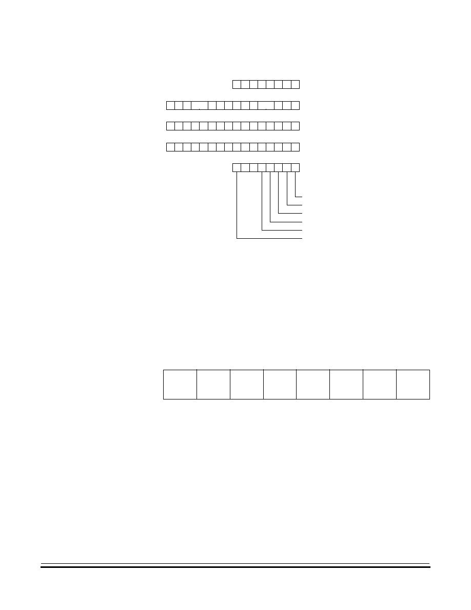
Central Processor Unit (CPU)
CPU Registers
MC68HC(7)08KH12
--
Rev. 1.0
Advance Information
MOTOROLA
Central Processor Unit (CPU)
53
Figure 6-1. CPU Registers
6.4.1 Accumulator (A)
The accumulator is a general-purpose 8-bit register. The CPU uses the
accumulator to hold operands and the results of arithmetic/logic
operations.
ACCUMULATOR (A)
INDEX REGISTER (H:X)
STACK POINTER (SP)
PROGRAM COUNTER (PC)
CONDITION CODE REGISTER (CCR)
CARRY/BORROW FLAG
ZERO FLAG
NEGATIVE FLAG
INTERRUPT MASK
HALF-CARRY FLAG
TWO'S COMPLEMENT OVERFLOW FLAG
V 1 1 H
I
N Z C
H
X
0
0
0
0
7
15
15
15
7
0
Bit 7
6
5
4
3
2
1
Bit 0
Read:
Write:
Reset:
Unaffected by reset
Figure 6-2. Accumulator (A)

Central Processor Unit (CPU)
Advance Information
MC68HC(7)08KH12
--
Rev. 1.0
54
Central Processor Unit (CPU)
MOTOROLA
6.4.2 Index Register (H:X)
The 16-bit index register allows indexed addressing of a 64-Kbyte
memory space. H is the upper byte of the index register, and X is the
lower byte. H:X is the concatenated 16-bit index register.
In the indexed addressing modes, the CPU uses the contents of the
index register to determine the conditional address of the operand.
The index register can serve also as a temporary data storage location.
Bit
15
14
13
12
11
10
9
8
7
6
5
4
3
2
1
Bit
0
Read:
Write:
Reset:
0
0
0
0
0
0
0
0
X
X
X
X
X
X
X
X
X = Indeterminate
Figure 6-3. Index Register (H:X)

Central Processor Unit (CPU)
CPU Registers
MC68HC(7)08KH12
--
Rev. 1.0
Advance Information
MOTOROLA
Central Processor Unit (CPU)
55
6.4.3 Stack Pointer (SP)
The stack pointer is a 16-bit register that contains the address of the next
location on the stack. During a reset, the stack pointer is preset to
$00FF. The reset stack pointer (RSP) instruction also sets the least
significant byte to $FF but does not affect the most significant byte. The
stack pointer decrements as data is pushed onto the stack and
increments as data is pulled from the stack.
In the stack pointer 8-bit offset and 16-bit offset addressing modes, the
stack pointer can function as an index register to access data on the
stack. The CPU uses the contents of the stack pointer to determine the
conditional address of the operand.
NOTE:
The location of the stack is arbitrary and may be relocated anywhere in
RAM. Moving the SP out of page zero ($0000 to $00FF) frees direct
address (page zero) space. For correct operation, the stack pointer must
point only to RAM locations.
Bit
15
14
13
12
11
10
9
8
7
6
5
4
3
2
1
Bit
0
Read:
Write:
Reset:
0
0
0
0
0
0
0
0
1
1
1
1
1
1
1
1
Figure 6-4. Stack Pointer (SP)

Central Processor Unit (CPU)
Advance Information
MC68HC(7)08KH12
--
Rev. 1.0
56
Central Processor Unit (CPU)
MOTOROLA
6.4.4 Program Counter (PC)
The program counter is a 16-bit register that contains the address of the
next instruction or operand to be fetched.
Normally, the program counter automatically increments to the next
sequential memory location every time an instruction or operand is
fetched. Jump, branch, and interrupt operations load the program
counter with an address other than that of the next sequential location.
During reset, the program counter is loaded with the reset vector
address located at $FFFE and $FFFF. The vector address is the
address of the first instruction to be executed after exiting the reset state.
Bit
15
14
13
12
11
10
9
8
7
6
5
4
3
2
1
Bit
0
Read:
Write:
Reset:
Loaded with vector from $FFFE and $FFFF
Figure 6-5. Program Counter (PC)

Central Processor Unit (CPU)
CPU Registers
MC68HC(7)08KH12
--
Rev. 1.0
Advance Information
MOTOROLA
Central Processor Unit (CPU)
57
6.4.5 Condition Code Register (CCR)
The 8-bit condition code register contains the interrupt mask and five
flags that indicate the results of the instruction just executed. Bits 6 and
5 are set permanently to logic one. The following paragraphs describe
the functions of the condition code register.
V -- Overflow Flag
The CPU sets the overflow flag when a two's complement overflow
occurs. The signed branch instructions BGT, BGE, BLE, and BLT use
the overflow flag.
1 = Overflow
0 = No overflow
H -- Half-Carry Flag
The CPU sets the half-carry flag when a carry occurs between
accumulator bits 3 and 4 during an ADD or ADC operation. The half-
carry flag is required for binary-coded decimal (BCD) arithmetic
operations. The DAA instruction uses the states of the H and C flags
to determine the appropriate correction factor.
1 = Carry between bits 3 and 4
0 = No carry between bits 3 and 4
Bit 7
6
5
4
3
2
1
Bit 0
Read:
V
1
1
H
I
N
Z
C
Write:
Reset:
X
1
1
X
1
X
X
X
X = Indeterminate
Figure 6-6. Condition Code Register (CCR)

Central Processor Unit (CPU)
Advance Information
MC68HC(7)08KH12
--
Rev. 1.0
58
Central Processor Unit (CPU)
MOTOROLA
I -- Interrupt Mask
When the interrupt mask is set, all maskable CPU interrupts are
disabled. CPU interrupts are enabled when the interrupt mask is
cleared. When a CPU interrupt occurs, the interrupt mask is set
automatically after the CPU registers are saved on the stack, but
before the interrupt vector is fetched.
1 = Interrupts disabled
0 = Interrupts enabled
NOTE:
To maintain M6805 compatibility, the upper byte of the index register (H)
is not stacked automatically. If the interrupt service routine modifies H,
then the user must stack and unstack H using the PSHH and PULH
instructions.
After the I bit is cleared, the highest-priority interrupt request is
serviced first.
A return from interrupt (RTI) instruction pulls the CPU registers from
the stack and restores the interrupt mask from the stack. After any
reset, the interrupt mask is set and can only be cleared by the clear
interrupt mask software instruction (CLI).
N -- Negative flag
The CPU sets the negative flag when an arithmetic operation, logic
operation, or data manipulation produces a negative result, setting bit
7 of the result.
1 = Negative result
0 = Non-negative result
Z -- Zero flag
The CPU sets the zero flag when an arithmetic operation, logic
operation, or data manipulation produces a result of $00.
1 = Zero result
0 = Non-zero result

Central Processor Unit (CPU)
Arithmetic/Logic Unit (ALU)
MC68HC(7)08KH12
--
Rev. 1.0
Advance Information
MOTOROLA
Central Processor Unit (CPU)
59
C -- Carry/Borrow Flag
The CPU sets the carry/borrow flag when an addition operation
produces a carry out of bit 7 of the accumulator or when a subtraction
operation requires a borrow. Some instructions -- such as bit test and
branch, shift, and rotate -- also clear or set the carry/borrow flag.
1 = Carry out of bit 7
0 = No carry out of bit 7
6.5 Arithmetic/Logic Unit (ALU)
The ALU performs the arithmetic and logic operations defined by the
instruction set.
Refer to the
CPU08 Reference Manual (Motorola document number
CPU08RM/AD) for a description of the instructions and addressing
modes and more detail about CPU architecture.

Central Processor Unit (CPU)
Advance Information
MC68HC(7)08KH12
--
Rev. 1.0
60
Central Processor Unit (CPU)
MOTOROLA

MC68HC(7)08KH12
--
Rev. 1.0
Advance Information
MOTOROLA
System Integration Module (SIM)
61
Advance Information -- MC68HC(7)08KH12
Section 7. System Integration Module (SIM)
7.1 Contents
7.2
Introduction . . . . . . . . . . . . . . . . . . . . . . . . . . . . . . . . . . . . . . . . 62
7.3
SIM Bus Clock Control and Generation . . . . . . . . . . . . . . . . . . 65
7.3.1
Bus Timing . . . . . . . . . . . . . . . . . . . . . . . . . . . . . . . . . . . . . 65
7.3.2
Clock Start-Up from POR . . . . . . . . . . . . . . . . . . . . . . . . . . 66
7.3.3
Clocks in Stop Mode and Wait Mode . . . . . . . . . . . . . . . . . 66
7.4
Reset and System Initialization. . . . . . . . . . . . . . . . . . . . . . . . . 66
7.4.1
External Pin Reset. . . . . . . . . . . . . . . . . . . . . . . . . . . . . . . . 67
7.4.2
Active Resets from Internal Sources . . . . . . . . . . . . . . . . . . 67
7.4.2.1
Power-On Reset . . . . . . . . . . . . . . . . . . . . . . . . . . . . . . . 68
7.4.2.2
Computer Operating Properly (COP) Reset . . . . . . . . . . 69
7.4.2.3
Illegal Opcode Reset . . . . . . . . . . . . . . . . . . . . . . . . . . . . 70
7.4.2.4
Illegal Address Reset . . . . . . . . . . . . . . . . . . . . . . . . . . . . 70
7.4.2.5
Universal Serial Bus Reset . . . . . . . . . . . . . . . . . . . . . . . 70
7.5
SIM Counter . . . . . . . . . . . . . . . . . . . . . . . . . . . . . . . . . . . . . . . 71
7.5.1
SIM Counter During Power-On Reset . . . . . . . . . . . . . . . . . 71
7.5.2
SIM Counter During Stop Mode Recovery . . . . . . . . . . . . . 71
7.5.3
SIM Counter and Reset States . . . . . . . . . . . . . . . . . . . . . . 71
7.6
Exception Control . . . . . . . . . . . . . . . . . . . . . . . . . . . . . . . . . . . 72
7.6.1
Interrupts . . . . . . . . . . . . . . . . . . . . . . . . . . . . . . . . . . . . . . . 72
7.6.1.1
Hardware Interrupts . . . . . . . . . . . . . . . . . . . . . . . . . . . . . 74
7.6.1.2
SWI Instruction. . . . . . . . . . . . . . . . . . . . . . . . . . . . . . . . . 76
7.6.2
Interrupt Status Registers . . . . . . . . . . . . . . . . . . . . . . . . . . 76
7.6.2.1
Interrupt Status Register 1 . . . . . . . . . . . . . . . . . . . . . . . . 77
7.6.2.2
Interrupt Status Register 2 . . . . . . . . . . . . . . . . . . . . . . . . 78
7.6.2.3
Interrupt Status Register 3 . . . . . . . . . . . . . . . . . . . . . . . . 78
7.6.3
Reset . . . . . . . . . . . . . . . . . . . . . . . . . . . . . . . . . . . . . . . . . . 79
7.6.4
Break Interrupts. . . . . . . . . . . . . . . . . . . . . . . . . . . . . . . . . . 79
7.6.5
Status Flag Protection in Break Mode. . . . . . . . . . . . . . . . . 79

System Integration Module (SIM)
Advance Information
MC68HC(7)08KH12
--
Rev. 1.0
62
System Integration Module (SIM)
MOTOROLA
7.7
Low-Power Modes . . . . . . . . . . . . . . . . . . . . . . . . . . . . . . . . . . 79
7.7.1
Wait Mode . . . . . . . . . . . . . . . . . . . . . . . . . . . . . . . . . . . . . . 80
7.7.2
Stop Mode . . . . . . . . . . . . . . . . . . . . . . . . . . . . . . . . . . . . . . 81
7.8
SIM Registers . . . . . . . . . . . . . . . . . . . . . . . . . . . . . . . . . . . . . . 83
7.8.1
Break Status Register (BSR). . . . . . . . . . . . . . . . . . . . . . . . 83
7.8.2
Reset Status Register (RSR) . . . . . . . . . . . . . . . . . . . . . . . 84
7.8.3
Break Flag Control Register (BFCR). . . . . . . . . . . . . . . . . . 85
7.2 Introduction
This section describes the system integration module (SIM), which
supports up to 24 external and/or internal interrupts. Together with the
CPU, the SIM controls all MCU activities. A block diagram of the SIM is
shown in
Figure 7-1
.
Figure 7-2
is a summary of the SIM I/O registers.
The SIM is a system state controller that coordinates CPU and exception
timing. The SIM is responsible for:
∑
Bus clock generation and control for CPU and peripherals
≠
top/wait/reset/break entry and recovery
≠
Internal clock control
∑
Master reset control, including power-on reset (POR) and COP
timeout
∑
Interrupt control:
≠
Acknowledge timing
≠
Arbitration control timing
≠
Vector address generation
∑
CPU enable/disable timing
∑
Modular architecture expandable to 128 interrupt sources
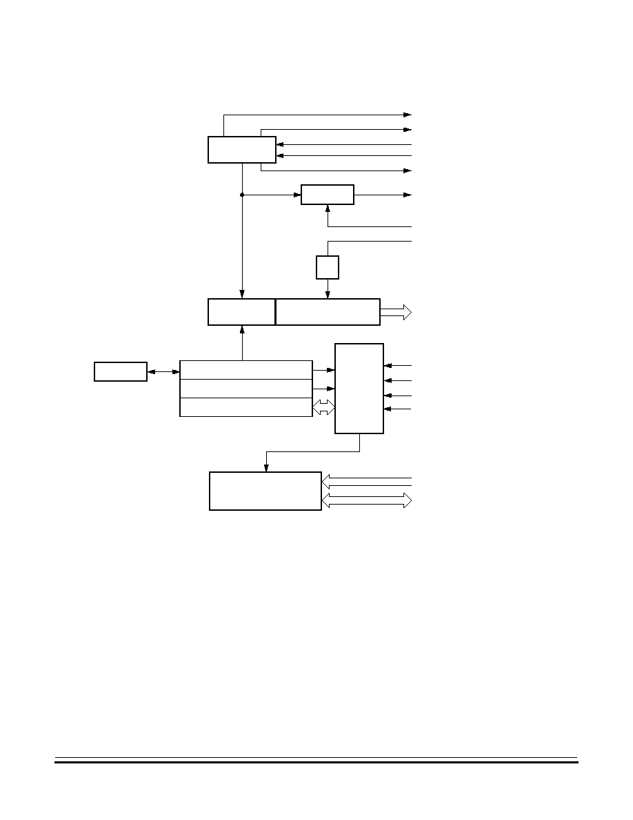
System Integration Module (SIM)
Introduction
MC68HC(7)08KH12
--
Rev. 1.0
Advance Information
MOTOROLA
System Integration Module (SIM)
63
Figure 7-1. SIM Block Diagram
STOP/WAIT
CLOCK
CONTROL
CLOCK GENERATORS
POR CONTROL
RESET PIN CONTROL
SIM RESET STATUS REGISTER
INTERRUPT CONTROL
AND PRIORITY DECODE
MODULE STOP
MODULE WAIT
CPU STOP (FROM CPU)
CPU WAIT (FROM CPU)
SIMOSCEN (TO CGM)
CGMOUT (FROM CGM)
INTERNAL CLOCKS
MASTER
RESET
CONTROL
RESET
PIN LOGIC
ILLEGAL OPCODE (FROM CPU)
ILLEGAL ADDRESS (FROM ADDRESS
MAP DECODERS)
COP TIMEOUT (FROM COP MODULE)
INTERRUPT SOURCES
CPU INTERFACE
RESET
CONTROL
SIM
COUNTER
COP CLOCK
CGMXCLK (FROM CGM)
˜
2
USB RESET (FROM USB MODULE)
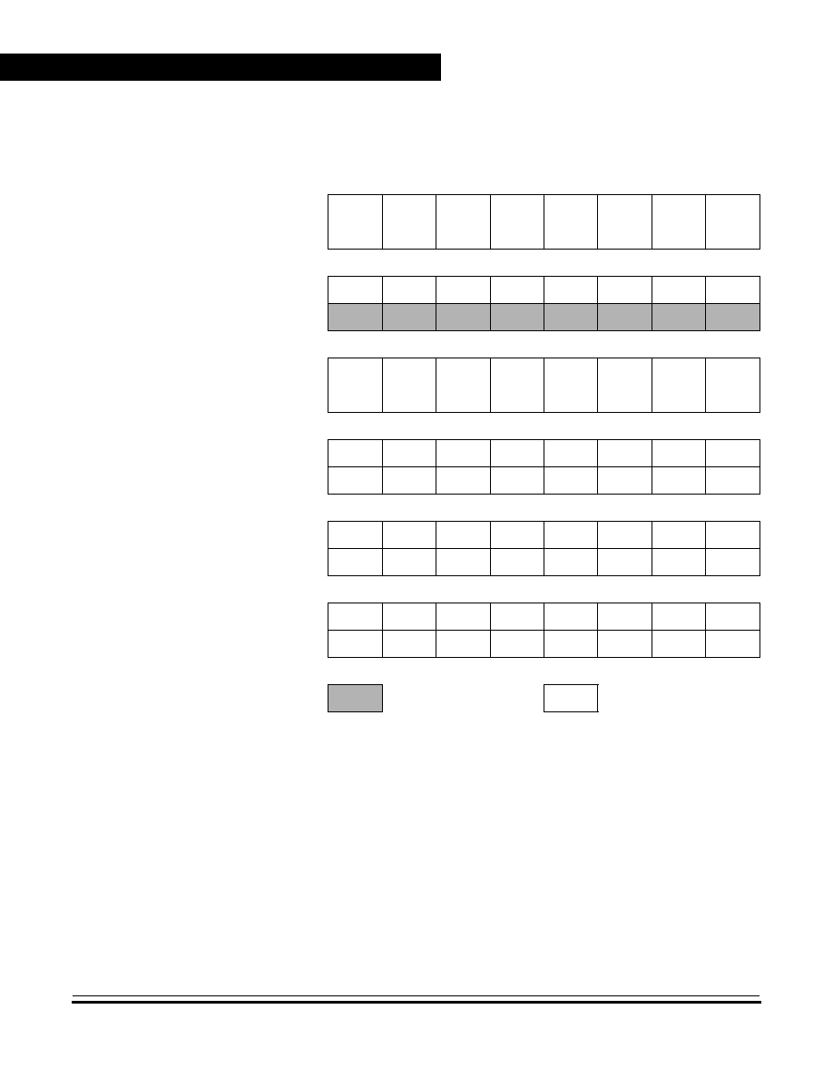
System Integration Module (SIM)
Advance Information
MC68HC(7)08KH12
--
Rev. 1.0
64
System Integration Module (SIM)
MOTOROLA
Addr.
Register Name
Bit 7
6
5
4
3
2
1
Bit 0
$FE00
Break Status Register
(BSR)
Read:
R
R
R
R
R
R
SBSW
R
Write:
Reset:
0
$FE01
Reset Status Register
(RSR)
Read:
POR
PIN
COP
ILOP
ILAD
USB
0
0
Write:
Reset:
1
0
0
0
0
0
0
0
$FE03
Break Flag Control Register
(BFCR)
Read:
BCFE
R
R
R
R
R
R
R
Write:
Reset:
0
$FE04
Interrupt Status Register 1
(INT1)
Read:
IF6
IF5
IF4
IF3
IF2
IF1
0
0
Write:
R
R
R
R
R
R
R
R
Reset:
0
0
0
0
0
0
0
0
$FE05
Interrupt Status Register 2
(INT2)
Read:
0
0
0
IF11
IF10
IF9
IF8
IF7
Write:
R
R
R
R
R
R
R
R
Reset:
0
0
0
0
0
0
0
0
$FE06
Interrupt Status Register 3
(INT3)
Read:
0
0
0
0
0
0
0
0
Write:
R
R
R
R
R
R
R
R
Reset:
0
0
0
0
0
0
0
0
= Unimplemented
R
= Reserved for factory test
Figure 7-2. SIM I/O Register Summary
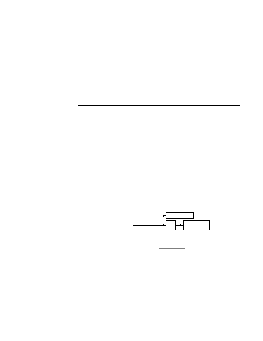
System Integration Module (SIM)
SIM Bus Clock Control and Generation
MC68HC(7)08KH12
--
Rev. 1.0
Advance Information
MOTOROLA
System Integration Module (SIM)
65
Table 7-1
shows the internal signal names used in this section.
7.3 SIM Bus Clock Control and Generation
The bus clock generator provides system clock signals for the CPU and
peripherals on the MCU. The system clocks are generated from an
incoming clock, CGMOUT, as shown in
Figure 7-3
.
Figure 7-3. SIM Clock Signals
7.3.1 Bus Timing
In user mode, the internal bus frequency is the oscillator frequency
(CGMXCLK) divided by four.
Table 7-1. Signal Name Conventions
Signal Name
Description
CGMXCLK
Buffered OSC1 from the oscillator
CGMOUT
The CGMXCLK frequency divided by two. This signal is again
divided by two in the SIM to generate the internal bus clocks
(Bus clock = CGMXCLK divided by four)
IAB
Internal address bus
IDB
Internal data bus
PORRST
Signal from the power-on reset module to the SIM
IRST
Internal reset signal
R/W
Read/write signal
˜
2
BUS CLOCK
GENERATORS
SIM
SIM COUNTER
From
PLL/OSCILLATOR
From
PLL/OSCILLATOR
CGMOUT
CGMXCLK

System Integration Module (SIM)
Advance Information
MC68HC(7)08KH12
--
Rev. 1.0
66
System Integration Module (SIM)
MOTOROLA
7.3.2 Clock Start-Up from POR
When the power-on reset module generates a reset, the clocks to the
CPU and peripherals are inactive and held in an inactive phase until after
the 4096 CGMXCLK cycle POR timeout has completed. The RST pin is
driven low by the SIM during this entire period. The IBUS clocks start
upon completion of the timeout.
7.3.3 Clocks in Stop Mode and Wait Mode
Upon exit from stop mode by an interrupt, break, or reset, the SIM allows
CGMXCLK to clock the SIM counter. The CPU and peripheral clocks do
not become active until after the stop delay timeout. This timeout is
selectable as 4096 or 32 CGMXCLK cycles.
(See 7.7.2 Stop Mode
.)
In wait mode, the CPU clocks are inactive. The SIM also produces two
sets of clocks for other modules. Refer to the wait mode subsection of
each module to see if the module is active or inactive in wait mode.
Some modules can be programmed to be active in wait mode.
7.4 Reset and System Initialization
The MCU has these reset sources:
∑
Power-on reset module (POR)
∑
External reset pin (RST)
∑
Computer operating properly module (COP)
∑
Illegal opcode
∑
Illegal address
∑
Universal Serial Bus module (USB)
All of these resets produce the vector $FFFE≠FFFF ($FEFE≠FEFF in
monitor mode) and assert the internal reset signal (IRST). IRST causes
all registers to be returned to their default values and all modules to be
returned to their reset states.
System Integration Module (SIM)
Reset and System Initialization
MC68HC(7)08KH12
--
Rev. 1.0
Advance Information
MOTOROLA
System Integration Module (SIM)
67
An internal reset clears the SIM counter
(see 7.5 SIM Counter
), but an
external reset does not. Each of the resets sets a corresponding bit in
the reset status register (RSR).
(See 7.8 SIM Registers
.)
7.4.1 External Pin Reset
The RST pin circuits include an internal pullup device. Pulling the
asynchronous RST pin low halts all processing. The PIN bit of the reset
status register (RSR) is set as long as RST is held low for a minimum of
67 CGMXCLK cycles, assuming that the POR was not the source of the
reset. See
Table 7-2
for details.
Figure 7-4
shows the relative timing.
Figure 7-4. External Reset Timing
7.4.2 Active Resets from Internal Sources
All internal reset sources actively pull the RST pin low for 32 CGMXCLK
cycles to allow resetting of external peripherals. The internal reset signal
IRST continues to be asserted for an additional 32 cycles.
See Figure 7-
5
. An internal reset can be caused by an illegal address, illegal opcode,
COP timeout, or POR.
(See Figure 7-6. Sources of Internal Reset
.)
Note that for POR resets, the SIM cycles through 4096 CGMXCLK
cycles during which the SIM forces the RST pin low. The internal reset
signal then follows the sequence from the falling edge of RST shown in
Figure 7-5
.
Table 7-2. PIN Bit Set Timing
Reset Type
Number of Cycles Required to Set PIN
POR
4163 (4096 + 64 + 3)
All others
67 (64 + 3)
RST
IAB
PC
VECT H
VECT L
CGMOUT
System Integration Module (SIM)
Advance Information
MC68HC(7)08KH12
--
Rev. 1.0
68
System Integration Module (SIM)
MOTOROLA
Figure 7-5. Internal Reset Timing
The COP reset is asynchronous to the bus clock.
Figure 7-6. Sources of Internal Reset
The active reset feature allows the part to issue a reset to peripherals
and other chips within a system built around the MCU.
7.4.2.1 Power-On Reset
When power is first applied to the MCU, the power-on reset module
(POR) generates a pulse to indicate that power-on has occurred. The
external reset pin (RST) is held low while the SIM counter counts out
4096 CGMXCLK cycles. Sixty-four CGMXCLK cycles later, the CPU and
memories are released from reset to allow the reset vector sequence to
occur. At power-on, the following events occur:
∑
A POR pulse is generated.
∑
The internal reset signal is asserted.
∑
The SIM enables the oscillator to drive CGMXCLK.
∑
Internal clocks to the CPU and modules are held inactive for 4096
CGMXCLK cycles to allow stabilization of the oscillator.
∑
The RST pin is driven low during the oscillator stabilization time.
∑
The POR bit of the reset status register (RSR) is set and all other
bits in the register are cleared.
IRST
RST
RST PULLED LOW BY MCU
IAB
32 CYCLES
32 CYCLES
VECTOR HIGH
CGMXCLK
ILLEGAL ADDRESS RST
ILLEGAL OPCODE RST
COPRST
POR
INTERNAL RESET
USB
System Integration Module (SIM)
Reset and System Initialization
MC68HC(7)08KH12
--
Rev. 1.0
Advance Information
MOTOROLA
System Integration Module (SIM)
69
Figure 7-7. POR Recovery
7.4.2.2 Computer Operating Properly (COP) Reset
An input to the SIM is reserved for the COP reset signal. The overflow of
the COP counter causes an internal reset and sets the COP bit in the
reset status register (RSR). The SIM actively pulls down the RST pin for
all internal reset sources.
To prevent a COP module timeout, write any value to location $FFFF.
Writing to location $FFFF clears the COP counter and stages 12 through
5 of the SIM counter. The SIM counter output, which occurs at least
every 2
12
≠ 2
4
CGMXCLK cycles, drives the COP counter. The COP
should be serviced as soon as possible out of reset to guarantee the
maximum amount of time before the first timeout.
The COP module is disabled if the RST pin or the IRQ1/V
PP
pin is held
at V
DD
+ V
HI
while the MCU is in monitor mode. The COP module can
be disabled only through combinational logic conditioned with the high
voltage signal on the RST or the IRQ1/V
PP
pin. This prevents the COP
from becoming disabled as a result of external noise. During a break
state, V
DD
+ V
HI
on the RST pin disables the COP module.
PORRST
OSC1
CGMXCLK
CGMOUT
RST
IAB
4096
CYCLES
32
CYCLES
32
CYCLES
$FFFE
$FFFF

System Integration Module (SIM)
Advance Information
MC68HC(7)08KH12
--
Rev. 1.0
70
System Integration Module (SIM)
MOTOROLA
7.4.2.3 Illegal Opcode Reset
The SIM decodes signals from the CPU to detect illegal instructions. An
illegal instruction sets the ILOP bit in the reset status register (RSR) and
causes a reset.
If the stop enable bit, STOP, in the mask option register is logic zero, the
SIM treats the STOP instruction as an illegal opcode and causes an
illegal opcode reset. The SIM actively pulls down the RST pin for all
internal reset sources.
7.4.2.4 Illegal Address Reset
An opcode fetch from an unmapped address generates an illegal
address reset. The SIM verifies that the CPU is fetching an opcode prior
to asserting the ILAD bit in the reset status register (RSR) and resetting
the MCU. A data fetch from an unmapped address does not generate a
reset. The SIM actively pulls down the RST pin for all internal reset
sources.
7.4.2.5 Universal Serial Bus Reset
The USB module will detect a reset signal on the bus by the presence of
an extended SE0 at the USB data pins of the upstream port. The reset
signaling is specified to be present for a minimum of 10 ms. An active
device (powered and not in the suspend state) seeing a single-ended
zero on its USB data inputs for more than 2.5
µ
s may treat that signal as
a reset, but must have interpreted the signaling as a reset within 5.5
µ
s.
For USB device, an SE0 condition between 4 and 8 low speed bit times
or 32 and 64 high speed bit times represents a valid USB reset. After the
reset is removed, the device will be in the attached, but not yet
addressed or configured state (refer to Section 9.1 of the USB
specification). The device must be able to accept device address via a
SET_ADDRESS command (refer to section 9.4 of the USB specification)
no later than 10 ms after the reset is removed.
Reset can wake a device from the suspended mode. A device may take
up to 10 ms to wake up from the suspended state.

System Integration Module (SIM)
SIM Counter
MC68HC(7)08KH12
--
Rev. 1.0
Advance Information
MOTOROLA
System Integration Module (SIM)
71
7.5 SIM Counter
The SIM counter is used by the power-on reset module (POR) and in
stop mode recovery to allow the oscillator time to stabilize before
enabling the internal bus (IBUS) clocks. The SIM counter also serves as
a prescalar for the computer operating properly module (COP). The SIM
counter uses 12 stages for counting, followed by a 13th stage that
triggers a reset of SIM counters and supplies the clock for the COP
module. The SIM counter is clocked by the falling edge of CGMXCLK.
7.5.1 SIM Counter During Power-On Reset
The power-on reset module (POR) detects power applied to the MCU.
At power-on, the POR circuit asserts the signal PORRST. Once the SIM
is initialized, it enables the oscillator to drive the bus clock state machine.
7.5.2 SIM Counter During Stop Mode Recovery
The SIM counter also is used for stop mode recovery. The STOP
instruction clears the SIM counter. After an interrupt, break, or reset, the
SIM senses the state of the short stop recovery bit, SSREC, in the mask
option register. If the SSREC bit is a logic one, then the stop recovery is
reduced from the normal delay of 4096 CGMXCLK cycles down to 32
CGMXCLK cycles. This is ideal for applications using canned oscillators
that do not require long start-up times from stop mode. External crystal
applications should use the full stop recovery time, that is, with SSREC
cleared in the configuration register (CONFIG).
7.5.3 SIM Counter and Reset States
External reset has no effect on the SIM counter. (
See 7.7.2 Stop Mode
for details.) The SIM counter is free-running after all reset states. (
See
7.4.2 Active Resets from Internal Sources
for counter control and
internal reset recovery sequences.)

System Integration Module (SIM)
Advance Information
MC68HC(7)08KH12
--
Rev. 1.0
72
System Integration Module (SIM)
MOTOROLA
7.6 Exception Control
Normal, sequential program execution can be changed in three different
ways:
∑
Interrupts
≠
Maskable hardware CPU interrupts
≠
Non-maskable software interrupt instruction (SWI)
∑
Reset
∑
Break interrupts
7.6.1 Interrupts
An interrupt temporarily changes the sequence of program execution to
respond to a particular event.
Figure 7-8
flow charts the handling of
system interrupts.
Interrupts are latched, and arbitration is performed in the SIM at the start
of interrupt processing. The arbitration result is a constant that the CPU
uses to determine which vector to fetch. Once an interrupt is latched by
the SIM, no other interrupt can take precedence, regardless of priority,
until the latched interrupt is serviced (or the I bit is cleared).
System Integration Module (SIM)
Exception Control
MC68HC(7)08KH12
--
Rev. 1.0
Advance Information
MOTOROLA
System Integration Module (SIM)
73
Figure 7-8. Interrupt Processing
NO
NO
NO
YES
NO
NO
YES
NO
YES
YES
FROM RESET
BREAK
I BIT SET?
IRQ1
INTERRUPT?
USB
INTERRUPT?
FETCH NEXT
INSTRUCTION
UNSTACK CPU REGISTERS.
STACK CPU REGISTERS
SET I BIT
LOAD PC WITH INTERRUPT VECTOR
EXECUTE INSTRUCTION.
YES
YES
I BIT SET?
INTERRUPT?
YES
OTHER
INTERRUPTS?
NO
SWI
INSTRUCITON?
RTI
INSTRUCITON?
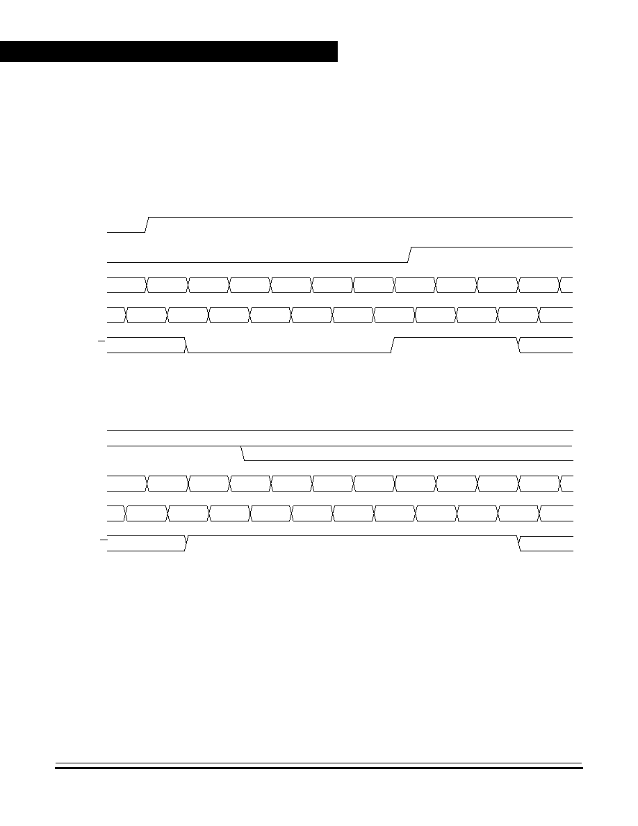
System Integration Module (SIM)
Advance Information
MC68HC(7)08KH12
--
Rev. 1.0
74
System Integration Module (SIM)
MOTOROLA
At the beginning of an interrupt, the CPU saves the CPU register
contents on the stack and sets the interrupt mask (I bit) to prevent
additional interrupts. At the end of an interrupt, the RTI instruction
recovers the CPU register contents from the stack so that normal
processing can resume.
Figure 7-9
shows interrupt entry timing.
Figure
7-10
shows interrupt recovery timing.
Figure 7-9
.
Interrupt Entry
Figure 7-10. Interrupt Recovery
7.6.1.1 Hardware Interrupts
A hardware interrupt does not stop the current instruction. Processing of
a hardware interrupt begins after completion of the current instruction.
When the current instruction is complete, the SIM checks all pending
hardware interrupts. If interrupts are not masked (I bit clear in the
condition code register), and if the corresponding interrupt enable bit is
MODULE
IDB
R/W
INTERRUPT
DUMMY
SP
SP ≠ 1
SP ≠ 2
SP ≠ 3
SP ≠ 4
VECT H
VECT L
START ADDR
IAB
DUMMY
PC ≠ 1[7:0] PC ≠ 1[15:8]
X
A
CCR
V DATA H
V DATA L
OPCODE
I BIT
MODULE
IDB
R/W
INTERRUPT
SP ≠ 4
SP ≠ 3
SP ≠ 2
SP ≠ 1
SP
PC
PC + 1
IAB
CCR
A
X
PC ≠ 1[7:0] PC ≠ 1[15:8] OPCODE
OPERAND
I BIT
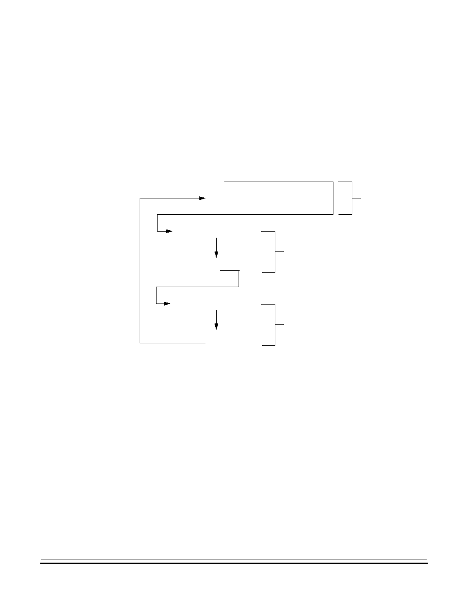
System Integration Module (SIM)
Exception Control
MC68HC(7)08KH12
--
Rev. 1.0
Advance Information
MOTOROLA
System Integration Module (SIM)
75
set, the SIM proceeds with interrupt processing; otherwise, the next
instruction is fetched and executed.
If more than one interrupt is pending at the end of an instruction
execution, the highest priority interrupt is serviced first.
Figure 7-11
demonstrates what happens when two interrupts are pending. If an
interrupt is pending upon exit from the original interrupt service routine,
the pending interrupt is serviced before the LDA instruction is executed.
Figure 7-11
.
Interrupt Recognition Example
The LDA opcode is prefetched by both the INT1 and INT2 RTI
instructions. However, in the case of the INT1 RTI prefetch, this is a
redundant operation.
NOTE:
To maintain compatibility with the M6805 Family, the H register is not
pushed on the stack during interrupt entry. If the interrupt service routine
modifies the H register or uses the indexed addressing mode, software
should save the H register and then restore it prior to exiting the routine.
CLI
LDA
INT1
PULH
RTI
INT2
BACKGROUND ROUTINE
#$FF
PSHH
INT1 INTERRUPT SERVICE ROUTINE
PULH
RTI
PSHH
INT2 INTERRUPT SERVICE ROUTINE
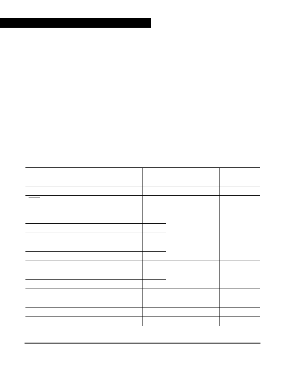
System Integration Module (SIM)
Advance Information
MC68HC(7)08KH12
--
Rev. 1.0
76
System Integration Module (SIM)
MOTOROLA
7.6.1.2 SWI Instruction
The SWI instruction is a non-maskable instruction that causes an
interrupt regardless of the state of the interrupt mask (I bit) in the
condition code register.
NOTE:
A software interrupt pushes PC onto the stack. A software interrupt does
not push PC ≠ 1, as a hardware interrupt does.
7.6.2 Interrupt Status Registers
The flags in the interrupt status registers identify maskable interrupt
sources.
Table 7-3
summarizes the interrupt sources and the interrupt
status register flags that they set. The interrupt status registers can be
useful for debugging.
Table 7-3. Interrupt Sources
Source
Flag
Mask
(1)
INT
Register
Flag
Priority
(2)
Vector Address
SWI Instruction
--
0
$FFFC≠$FFFD
IRQ1 Pin
IRQF1
IMASK1
IF1
1
$FFFA≠$FFFB
HUB Start of Frame Interrupt
SOFF
SOFIE
IF2
2
$FFF8≠$FFF9
HUB 2nd End of Frame Point Interrupt
EOF2F
EOF2IE
HUB End of Packet Interrupt
EOPF
EOPIE
HUB Bus Signal Transition Detect Interrupt
TRANF
TRANIE
HUB Endpoint0 Transmit Interrupt
TXDF
TXDIE
IF3
3
$FFF6≠$FFF7
HUB Endpoint0 Receive Interrupt
RXDF
RXDIE
Device Endpoint 0 Transmit Interrupt
TXD0F
TXD0IE
IF4
4
$FFF4≠$FFF5
Device Endpoint 0 Receive Interrupt
RXD0F
RXD0IE
USB Endpoint1/2 Transmit Interrupt
TXD1F
TXD1IE
TIM Channel 0
CH0F
CH0IE
IF5
5
$FFF2≠$FFF3
TIM Channel 1
CH1F
CH1IE
IF6
6
$FFF0≠$FFF1
TIM Overflow
TOF
TOIE
IF7
7
$FFEE≠$FFEF
Port-E Keyboard Pin Interrupt
KEYEF
IMASKE
IF8
8
$FFEC≠$FFED
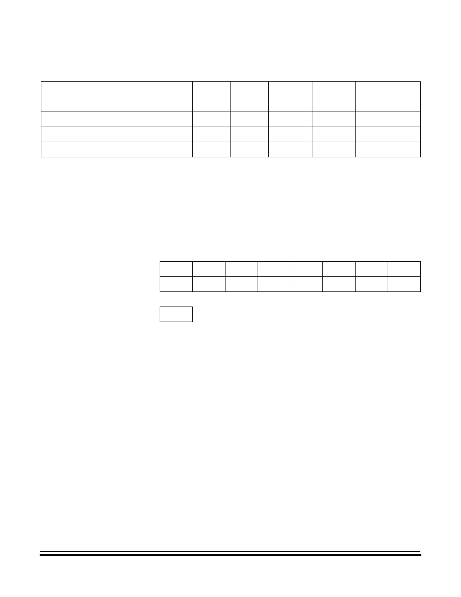
System Integration Module (SIM)
Exception Control
MC68HC(7)08KH12
--
Rev. 1.0
Advance Information
MOTOROLA
System Integration Module (SIM)
77
7.6.2.1 Interrupt Status Register 1
I
F
6≠I
F
1 -- Interrupt Flags 1≠6
These flags indicate the presence of interrupt requests from the
sources shown in
Table 7-3
.
1 = Interrupt request present
0 = No interrupt request present
Bit 0 and Bit 1 -- Always read 0
Port-D Keyboard Pin Interrupt
KEYDF
IMASKD
IF9
9
$FFEA≠$FFEB
Port-F Keyboard Pin Interrupt
KEYFF
IMASKF
IF10
10
$FFE8≠$FFE9
Phase-locked Loop Interrupt
PLLF
PLLIE
IF11
11
$FFE6≠$FFE7
(1) The I bit in the condition code register is a global mask for all interrupts sources except the SWI instruction.
(2) 0= highest priority
Table 7-3. Interrupt Sources
Source
Flag
Mask
(1)
INT
Register
Flag
Priority
(2)
Vector Address
Address:
$FE04
Bit 7
6
5
4
3
2
1
Bit 0
Read:
IF6
IF5
IF4
IF3
IF2
IF1
0
0
Write:
R
R
R
R
R
R
R
R
Reset:
0
0
0
0
0
0
0
0
R
= Reserved
Figure 7-12. Interrupt Status Register 1 (INT1)
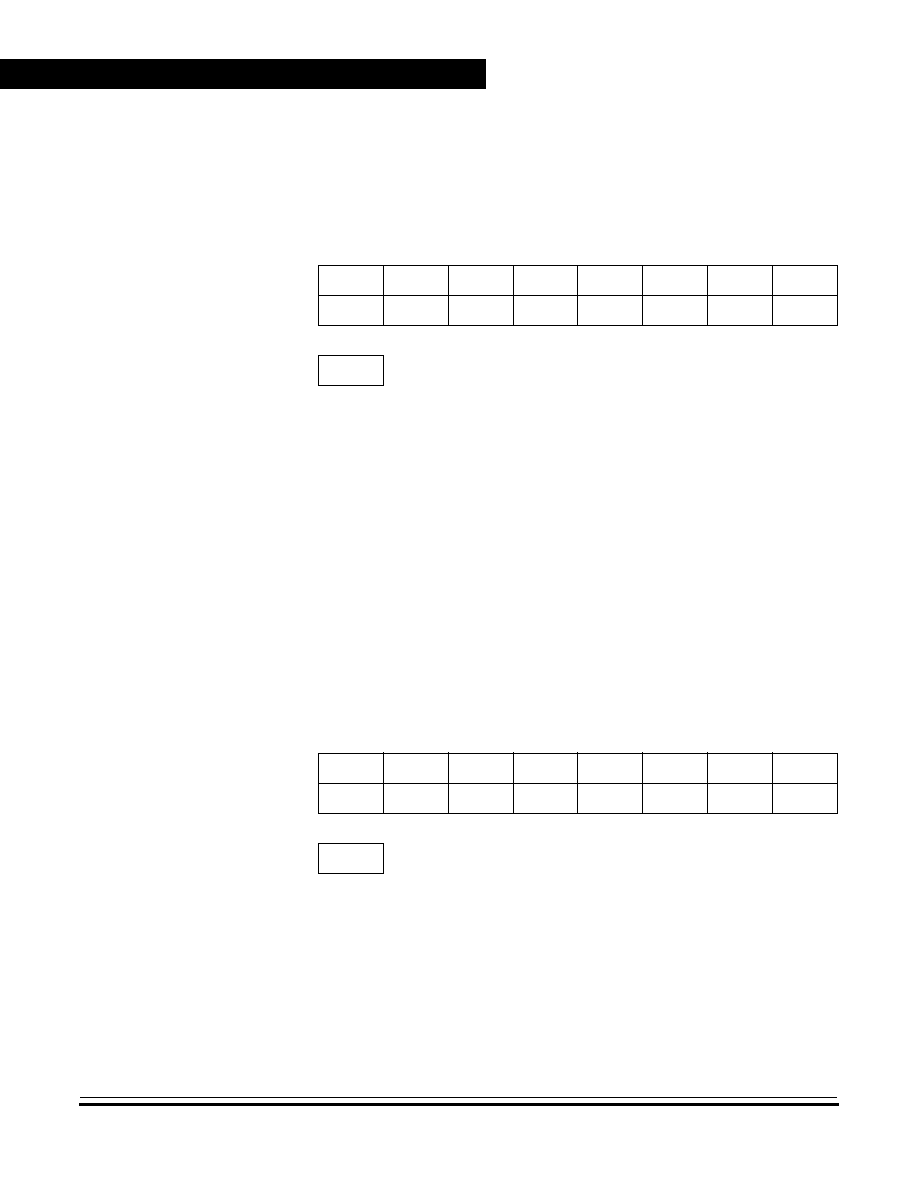
System Integration Module (SIM)
Advance Information
MC68HC(7)08KH12
--
Rev. 1.0
78
System Integration Module (SIM)
MOTOROLA
7.6.2.2 Interrupt Status Register 2
I
F
11≠I
F
7 -- Interrupt Flags 11≠7
These flags indicate the presence of interrupt requests from the
sources shown in
Table 7-3
.
1 = Interrupt request present
0 = No interrupt request present
7.6.2.3 Interrupt Status Register 3
Bits 7≠0 -- Always read 0
Address:
$FE05
Bit 7
6
5
4
3
2
1
Bit 0
Read:
0
0
0
IF11
IF10
IF9
IF8
IF7
Write:
R
R
R
R
R
R
R
R
Reset:
0
0
0
0
0
0
0
0
R
= Reserved
Figure 7-13. Interrupt Status Register 2 (INT2)
Address:
$FE06
Bit 7
6
5
4
3
2
1
Bit 0
Read:
0
0
0
0
0
0
0
0
Write:
R
R
R
R
R
R
R
R
Reset:
0
0
0
0
0
0
0
0
R
= Reserved
Figure 7-14. Interrupt Status Register 2 (INT2)

System Integration Module (SIM)
Low-Power Modes
MC68HC(7)08KH12
--
Rev. 1.0
Advance Information
MOTOROLA
System Integration Module (SIM)
79
7.6.3 Reset
All reset sources always have equal and highest priority and cannot be
arbitrated.
7.6.4 Break Interrupts
The break module can stop normal program flow at a software-
programmable break point by asserting its break interrupt output.
(See
Section 16. Break Module (BREAK)
.) The SIM puts the CPU into the
break state by forcing it to the SWI vector location. Refer to the break
interrupt subsection of each module to see how each module is affected
by the break state.
7.6.5 Status Flag Protection in Break Mode
The SIM controls whether status flags contained in other modules can
be cleared during break mode. The user can select whether flags are
protected from being cleared by properly initializing the break clear flag
enable bit (BCFE) in the break flag control register (BFCR).
Protecting flags in break mode ensures that set flags will not be cleared
while in break mode. This protection allows registers to be freely read
and written during break mode without losing status flag information.
Setting the BCFE bit enables the clearing mechanisms. Once cleared in
break mode, a flag remains cleared even when break mode is exited.
Status flags with a two-step clearing mechanism -- for example, a read
of one register followed by the read or write of another -- are protected,
even when the first step is accomplished prior to entering break mode.
Upon leaving break mode, execution of the second step will clear the
flag as normal.
7.7 Low-Power Modes
Executing the WAIT or STOP instruction puts the MCU in a low-power-
consumption mode for standby situations. The SIM holds the CPU in a
non-clocked state. The operation of each of these modes is described

System Integration Module (SIM)
Advance Information
MC68HC(7)08KH12
--
Rev. 1.0
80
System Integration Module (SIM)
MOTOROLA
below. Both STOP and WAIT clear the interrupt mask (I) in the condition
code register, allowing interrupts to occur.
7.7.1 Wait Mode
In wait mode, the CPU clocks are inactive while the peripheral clocks
continue to run.
Figure 7-15
shows the timing for wait mode entry.
A module that is active during wait mode can wake up the CPU with an
interrupt if the interrupt is enabled. Stacking for the interrupt begins one
cycle after the WAIT instruction during which the interrupt occurred. In
wait mode, the CPU clocks are inactive. Refer to the wait mode
subsection of each module to see if the module is active or inactive in
wait mode. Some modules can be programmed to be active in wait
mode.
Wait mode can also be exited by a reset or break. A break interrupt
during wait mode sets the SIM break stop/wait bit, SBSW, in the break
status register (BSR). If the COP disable bit, COPD, in the mask option
register is logic zero, then the computer operating properly module
(COP) is enabled and remains active in wait mode.
Figure 7-15. Wait Mode Entry Timing
Figure 7-16
and
Figure 7-17
show the timing for WAIT recovery.
WAIT ADDR + 1
SAME
SAME
IAB
IDB
PREVIOUS DATA
NEXT OPCODE
SAME
WAIT ADDR
SAME
R/W
NOTE: Previous data can be operand data or the WAIT opcode, depending on the
last instruction.
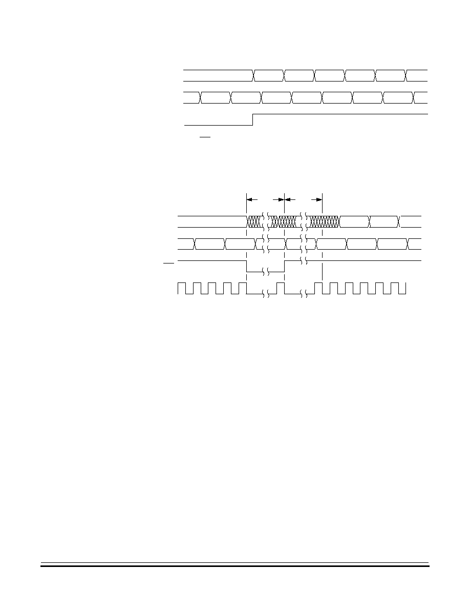
System Integration Module (SIM)
Low-Power Modes
MC68HC(7)08KH12
--
Rev. 1.0
Advance Information
MOTOROLA
System Integration Module (SIM)
81
Figure 7-16. Wait Recovery from Interrupt or Break
Figure 7-17. Wait Recovery from Internal Reset
7.7.2 Stop Mode
In stop mode, the SIM counter is reset and the system clocks are
disabled. An interrupt request from a module can cause an exit from stop
mode. Stacking for interrupts begins after the selected stop recovery
time has elapsed. Reset or break also causes an exit from stop mode.
The SIM disables the oscillator signals (CGMOUT and CGMXCLK) in
stop mode, stopping the CPU and peripherals. Stop recovery time is
selectable using the SSREC bit in the configuration register (CONFIG).
If SSREC is set, stop recovery is reduced from the normal delay of 4096
CGMXCLK cycles down to 32. This is ideal for applications using canned
oscillators that do not require long startup times from stop mode.
NOTE:
External crystal applications should use the full stop recovery time by
clearing the SSREC bit.
$6E0C
$6E0B
$00FF
$00FE
$00FD
$00FC
$A6
$A6
$01
$0B
$6E
$A6
IAB
IDB
EXITSTOPWAIT
NOTE: EXITSTOPWAIT = RST pin OR CPU interrupt OR break interrupt
IAB
IDB
RST
$A6
$A6
$6E0B
RST V CT H RST V CT L
$A6
CGMXCLKCGMXCLK
32
Cycles
32
Cycles
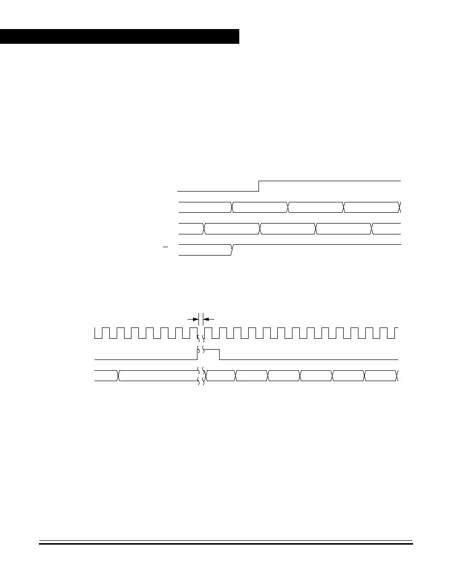
System Integration Module (SIM)
Advance Information
MC68HC(7)08KH12
--
Rev. 1.0
82
System Integration Module (SIM)
MOTOROLA
A break interrupt during stop mode sets the SIM break stop/wait bit
(SBSW) in the break status register (BSR).
The SIM counter is held in reset from the execution of the STOP
instruction until the beginning of stop recovery. It is then used to time the
recovery period.
Figure 7-18
shows stop mode entry timing.
NOTE:
To minimize stop current, all pins configured as inputs should be driven
to a logic 1 or logic 0.
Figure 7-18. Stop Mode Entry Timing
Figure 7-19. Stop Mode Recovery from Interrupt or Break
STOP ADDR + 1
SAME
SAME
IAB
IDB
PREVIOUS DATA
NEXT OPCODE
SAME
STOP ADDR
SAME
R/W
CPUSTOP
NOTE: Previous data can be operand data or the STOP opcode, depending on the last
instruction.
CGMXCLK
INT/BREAK
IAB
STOP + 2
STOP + 2
SP
SP ≠ 1
SP ≠ 2
SP ≠ 3
STOP +1
STOP RECOVERY PERIOD
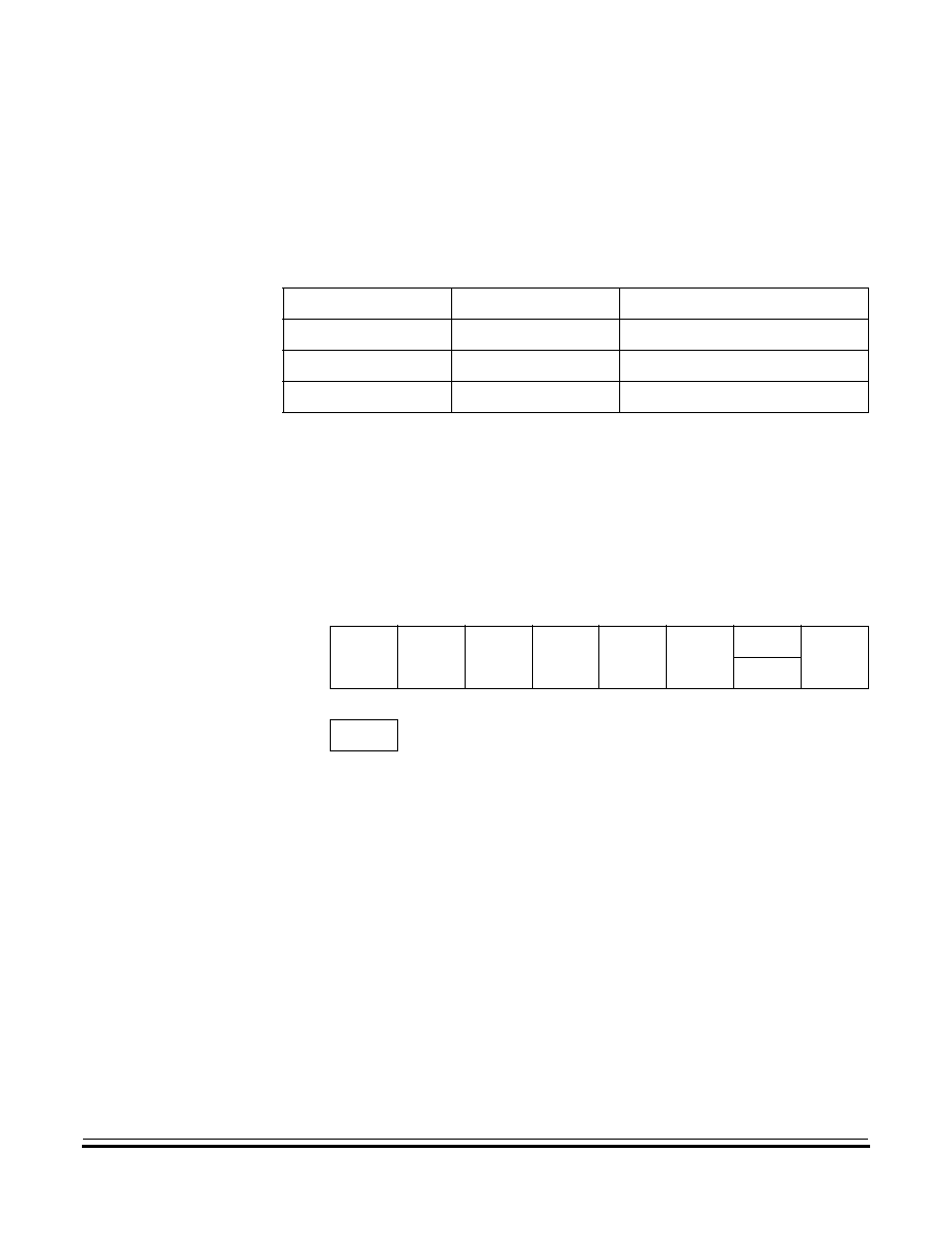
System Integration Module (SIM)
SIM Registers
MC68HC(7)08KH12
--
Rev. 1.0
Advance Information
MOTOROLA
System Integration Module (SIM)
83
7.8 SIM Registers
The SIM has three memory mapped registers.
Table 7-4
shows the
mapping of these registers.
7.8.1 Break Status Register (BSR)
The break status register contains a flag to indicate that a break caused
an exit from stop or wait mode.
SBSW -- SIM Break Stop/Wait
This status bit is useful in applications requiring a return to wait
or stop mode after exiting from a break interrupt. Clear SBSW
by writing a logic zero to it. Reset clears SBSW.
1 = Stop mode or wait mode was exited by break interrupt
0 = Stop mode or wait mode was not exited by break
interrupt
SBSW can be read within the break state SWI routine. The user can
modify the return address on the stack by subtracting one from it. The
following code is an example of this. Writing zero to the SBSW bit clears
it.
Table 7-4. SIM Registers
Address
Register
Access Mode
$FE00
BSR
User
$FE01
RSR
User
$FE03
BFCR
User
Address:
$FE00
Bit 7
6
5
4
3
2
1
Bit 0
Read:
R
R
R
R
R
R
SBSW
R
Write:
Note 1
Reset:
0
R
= Reserved
1. Writing a logic zero clears SBSW
Figure 7-20. Break Status Register (BSR)
System Integration Module (SIM)
Advance Information
MC68HC(7)08KH12
--
Rev. 1.0
84
System Integration Module (SIM)
MOTOROLA
7.8.2 Reset Status Register (RSR)
This register contains six flags that show the source of the last reset.
Clear the SIM reset status register by reading it. A power-on reset sets
the POR bit and clears all other bits in the register.
;
;
;
This code works if the H register has been pushed onto the stack in the break
service routine software. This code should be executed at the end of the
break service routine software.
HIBYTE
EQU
5
LOBYTE
EQU
6
;
If not SBSW, do RTI
BRCLR
SBSW,BSR, RETURN
;
;
See if wait mode or stop mode was exited
by break
TST
LOBYTE,SP
; If RETURNLO is not zero,
BNE
DOLO
; then just decrement low byte.
DEC
HIBYTE,SP
; Else deal with high byte, too.
DOLO
DEC
LOBYTE,SP
; Point to WAIT/STOP opcode.
RETURN
PULH
RTI
; Restore H register.
Address:
$FE01
Bit 7
6
5
4
3
2
1
Bit 0
Read:
POR
PIN
COP
ILOP
ILAD
USB
0
0
Write:
POR:
1
0
0
0
0
0
0
0
= Unimplemented
Figure 7-21. Reset Status Register (RSR)

System Integration Module (SIM)
SIM Registers
MC68HC(7)08KH12
--
Rev. 1.0
Advance Information
MOTOROLA
System Integration Module (SIM)
85
POR -- Power-On Reset Bit
1 = Last reset caused by POR circuit
0 = Read of RSR
PIN -- External Reset Bit
1 = Last reset caused by external reset pin (RST)
0 = POR or read of RSR
COP -- Computer Operating Properly Reset Bit
1 = Last reset caused by COP counter
0 = POR or read of RSR
ILOP -- Illegal Opcode Reset Bit
1 = Last reset caused by an illegal opcode
0 = POR or read of RSR
ILAD -- Illegal Address Reset Bit (opcode fetches only)
1 = Last reset caused by an opcode fetch from an illegal
address
0 = POR or read of RSR
USB --Universal Serial Bus Reset Bit
1 = Last reset caused by an USB module
0 = POR or read of RSR
7.8.3 Break Flag Control Register (BFCR)
The break control register contains a bit that enables software to clear
status bits while the MCU is in a break state.
Address:
$FE03
Bit 7
6
5
4
3
2
1
Bit 0
Read:
BCFE
R
R
R
R
R
R
R
Write:
Reset:
0
0
0
0
0
0
0
0
R
= Reserved
Figure 7-22. Break Flag Control Register (BFCR)

System Integration Module (SIM)
Advance Information
MC68HC(7)08KH12
--
Rev. 1.0
86
System Integration Module (SIM)
MOTOROLA
BCFE -- Break Clear Flag Enable Bit
This read/write bit enables software to clear status bits by
accessing status registers while the MCU is in a break state.
To clear status bits during the break state, the BCFE bit must
be set.
1 = Status bits clearable during break
0 = Status bits not clearable during break

MC68HC(7)08KH12
--
Rev. 1.0
Advance Information
MOTOROLA
Clock Generator Module (CGM)
87
Advance Information -- MC68HC(7)08KH12
Section 8. Clock Generator Module (CGM)
8.1 Contents
8.2
Introduction . . . . . . . . . . . . . . . . . . . . . . . . . . . . . . . . . . . . . . . . 88
8.3
Features . . . . . . . . . . . . . . . . . . . . . . . . . . . . . . . . . . . . . . . . . . 89
8.4
Functional Description . . . . . . . . . . . . . . . . . . . . . . . . . . . . . . . 89
8.4.1
Crystal Oscillator Circuit . . . . . . . . . . . . . . . . . . . . . . . . . . . 91
8.4.2
Phase-Locked Loop Circuit (PLL) . . . . . . . . . . . . . . . . . . . . 91
8.4.3
PLL Circuits . . . . . . . . . . . . . . . . . . . . . . . . . . . . . . . . . . . . . 91
8.4.4
Acquisition and Tracking Modes . . . . . . . . . . . . . . . . . . . . . 93
8.4.5
Manual and Automatic PLL Bandwidth Modes . . . . . . . . . . 93
8.4.6
Programming the PLL . . . . . . . . . . . . . . . . . . . . . . . . . . . . . 94
8.4.7
Special Programming Exceptions . . . . . . . . . . . . . . . . . . . . 95
8.4.8
Base Clock Selector Circuit. . . . . . . . . . . . . . . . . . . . . . . . . 96
8.4.9
CGM External Connections. . . . . . . . . . . . . . . . . . . . . . . . . 96
8.5
I/O Signals . . . . . . . . . . . . . . . . . . . . . . . . . . . . . . . . . . . . . . . . 98
8.5.1
Crystal Amplifier Input Pin (OSC1) . . . . . . . . . . . . . . . . . . . 98
8.5.2
Crystal Amplifier Output Pin (OSC2) . . . . . . . . . . . . . . . . . . 98
8.5.3
External Filter Capacitor Pin (CGMXFC). . . . . . . . . . . . . . . 98
8.5.4
PLL Analog Power Pin (V
DDA
) . . . . . . . . . . . . . . . . . . . . . . 98
8.5.5
PLL Analog Ground Pin (V
SSA
) . . . . . . . . . . . . . . . . . . . . . . 98
8.5.6
Buffered Crystal Clock Output (CGMVOUT) . . . . . . . . . . . . 99
8.5.7
CGMVSEL. . . . . . . . . . . . . . . . . . . . . . . . . . . . . . . . . . . . . . 99
8.5.8
Oscillator Enable Signal (SIMOSCEN) . . . . . . . . . . . . . . . . 99
8.5.9
Crystal Output Frequency Signal (CGMXCLK) . . . . . . . . . . 99
8.5.10
CGM Base Clock Output (CGMOUT) . . . . . . . . . . . . . . . . . 99
8.5.11
CGM CPU Interrupt (CGMINT) . . . . . . . . . . . . . . . . . . . . . . 99
8.6
CGM Registers . . . . . . . . . . . . . . . . . . . . . . . . . . . . . . . . . . . . 100
8.6.1
PLL Control Register (PCTL) . . . . . . . . . . . . . . . . . . . . . . 102
8.6.2
PLL Bandwidth Control Register (PBWC) . . . . . . . . . . . . . 104
8.6.3
PLL Multiplier Select Registers (PMSH:PMSL). . . . . . . . . 105

Clock Generator Module (CGM)
Advance Information
MC68HC(7)08KH12
--
Rev. 1.0
88
Clock Generator Module (CGM)
MOTOROLA
8.6.4
PLL Reference Divider Select Register (PRDS) . . . . . . . . 106
8.7
Interrupts. . . . . . . . . . . . . . . . . . . . . . . . . . . . . . . . . . . . . . . . . 107
8.8
Special Modes . . . . . . . . . . . . . . . . . . . . . . . . . . . . . . . . . . . . 107
8.8.1
Wait Mode . . . . . . . . . . . . . . . . . . . . . . . . . . . . . . . . . . . . . 107
8.8.2
CGM During Break Interrupts . . . . . . . . . . . . . . . . . . . . . . 108
8.9
Acquisition/Lock Time Specifications . . . . . . . . . . . . . . . . . . . 108
8.9.1
Acquisition/Lock Time Definitions . . . . . . . . . . . . . . . . . . . 108
8.9.2
Parametric Influences on Reaction Time . . . . . . . . . . . . . 109
8.9.3
Choosing a Filter Capacitor. . . . . . . . . . . . . . . . . . . . . . . . 111
8.9.4
Reaction Time Calculation . . . . . . . . . . . . . . . . . . . . . . . . 111
8.2 Introduction
This section describes the clock generator module (CGM). The CGM
generates the crystal clock signal, CGMXCLK, which operates at the
frequency of the crystal. The CGM also generates the base clock signal,
CGMOUT, which is based on either the crystal clock divided by two or
the phase-locked loop (PLL) clock, CGMPCLK, divided by two. This is
the clock from which the SIM derives the system clocks, including the
bus clock, which is at a frequency of CGMOUT/2. The PLL also
generates a CGMVCLK clock, at 48MHz, for use as the USBCLK. The
PLL is a fully functional frequency generator designed for use with
crystals or ceramic resonators.
This CGM is optimized to generate a 48MHz reference frequency for the
USB module, from a 6MHz crystal.

Clock Generator Module (CGM)
Features
MC68HC(7)08KH12
--
Rev. 1.0
Advance Information
MOTOROLA
Clock Generator Module (CGM)
89
8.3 Features
Features of the CGM include:
∑
VCO Center-Of-Range Frequuency tuned to 48MHz for Low-Jitter
Clock Reference for USB Module
∑
Low-Frequency Crystal Operation with Low-Power Operation and
High-Output Frequency Resolution
∑
Programmable Reference Divider for Even Greater Resolution
∑
Programmable Prescaler for Power-of-Two Increases in Bus
Frequency
∑
Automatic Bandwidth Control Mode for Low-Jitter Operation
∑
Automatic Frequency Lock Detector
∑
CPU Interrupt on Entry or Exit from Locked Condition
8.4 Functional Description
The CGM consists of three major submodules:
∑
Crystal oscillator circuit -- The crystal oscillator circuit generates
the constant crystal frequency clock, CGMXCLK.
∑
Phase-locked loop (PLL) -- The PLL generates the
programmable VCO frequency clock, CGMVCLK and CGMPCLK.
∑
Base clock selector circuit -- This software-controlled circuit
selects either CGMXCLK divided by two or the PLL clock,
CGMPCLK, divided by two as the base clock, CGMOUT. The SIM
derives the system clocks from CGMOUT.
Figure 8-1
shows the structure of the CGM.
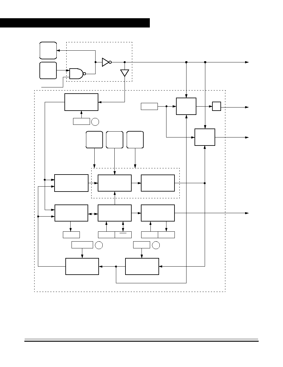
Clock Generator Module (CGM)
Advance Information
MC68HC(7)08KH12
--
Rev. 1.0
90
Clock Generator Module (CGM)
MOTOROLA
Figure 8-1. CGM Block Diagram
BCS
PHASE
DETECTOR
LOOP
FILTER
FREQUENCY
DIVIDER
VOLTAGE
CONTROLLED
OSCILLATOR
AUTOMATIC
MODE
CONTROL
LOCK
DETECTOR
CLOCK
CGMXCLK
CGMOUT
CGMVDV
CGMVCLK
SIMOSCEN
INTERRUPT
CONTROL
CGMINT
CGMRDV
PLL ANALOG
˜
2
CGMRCLK
OSC2
OSC1
SELECT
CIRCUIT
V
DDA
CGMXFC
V
SSA
LOCK
AUTO
ACQ
PLLIE
PLLF
MUL[11:0]
REFERENCE
DIVIDER
RDS[3:0]
FREQUENCY
DIVIDER
PRE[1:0]
CGMPCLK
USBCLK
P
N
R
CLOCK
SELECT
CIRCUIT
PHASE-LOCKED LOOP (PLL)
OSCILLATOR (OSC)
48MHz

Clock Generator Module (CGM)
Functional Description
MC68HC(7)08KH12
--
Rev. 1.0
Advance Information
MOTOROLA
Clock Generator Module (CGM)
91
8.4.1 Crystal Oscillator Circuit
The crystal oscillator circuit consists of an inverting amplifier and an
external crystal. The OSC1 pin is the input to the amplifier and the OSC2
pin is the output. The SIMOSCEN signal from the system integration
module (SIM) enables the crystal oscillator circuit.
The CGMXCLK signal is the output of the crystal oscillator circuit and
runs at a rate equal to the crystal frequency. CGMXCLK is then buffered
to produce CGMRCLK, the PLL reference clock.
CGMXCLK can be used by other modules which require precise timing
for operation. The duty cycle of CGMXCLK is not guaranteed to be 50%
and depends on external factors, including the crystal and related
external components. An externally generated clock also can feed the
OSC1 pin of the crystal oscillator circuit. Connect the external clock to
the OSC1 pin and let the OSC2 pin float.
8.4.2 Phase-Locked Loop Circuit (PLL)
The PLL is a frequency generator that can operate in either acquisition
mode or tracking mode, depending on the accuracy of the output
frequency. The PLL can change between acquisition and tracking
modes either automatically or manually.
8.4.3 PLL Circuits
The PLL consists of these circuits:
∑
Voltage-controlled oscillator (VCO)
∑
Reference divider
∑
Frequency prescaler
∑
Modulo VCO frequency divider
∑
Phase detector
∑
Loop filter
∑
Lock detector

Clock Generator Module (CGM)
Advance Information
MC68HC(7)08KH12
--
Rev. 1.0
92
Clock Generator Module (CGM)
MOTOROLA
The operating range of the VCO is programmable for a wide range of
frequencies and for maximum immunity to external noise, including
supply and CGM/XFC noise. The VCO frequency is bound to a range
from roughly 40MHz to 56MHz, f
VRS
. Modulating the voltage on the
CGM/XFC pin changes the frequency within this range. By design, f
VRS
is tuned to a nominal center-of-range frequency of 48MHz.
CGMRCLK is the PLL reference clock, a buffered version of CGMXCLK.
CGMRCLK runs at a frequency, f
RCLK
, and is fed to the PLL through a
programmable modulo reference divider, which divides f
RCLK
by a factor
R. This feature allows frequency steps of higher resolution. The divider's
output is the final reference clock, CGMRDV, running at a frequency
f
RDV
= f
RCLK
/R.
The VCO's output clock, CLK, running at a frequency f
VCLK
is fed back
through a programmable prescale divider and a programmable modulo
divider. The prescaler divides the VCO clock by a power-of-two factor P
and the modulo divider reduces the VCO clock by a factor, N. The
dividers' output is the VCO feedback clock, CGMVDV, running at a
frequency f
VDV
= f
VCLK
/(N
◊
2
P
). (See
8.4.6 Programming the PLL
for
more information.)
The phase detector then compares the VCO feedback clock, CGMVDV,
with the final reference clock, CGMRDV. A correction pulse is generated
based on the phase difference between the two signals. The loop filter
then slightly alters the DC voltage on the external capacitor connected
to CGM/XFC based on the width and direction of the correction pulse.
The filter can make fast or slow corrections depending on its mode,
described in
8.4.4 Acquisition and Tracking Modes
. The value of the
external capacitor and the reference frequency determines the speed of
the corrections and the stability of the PLL.
The lock detector compares the frequencies of the VCO feedback clock,
CGMVDV, and the final reference clock, CGMRDV. Therefore, the
speed of the lock detector is directly proportional to the final reference
frequency, f
RDV
. The circuit determines the mode of the PLL and the lock
condition based on this comparison.

Clock Generator Module (CGM)
Functional Description
MC68HC(7)08KH12
--
Rev. 1.0
Advance Information
MOTOROLA
Clock Generator Module (CGM)
93
8.4.4 Acquisition and Tracking Modes
The PLL filter is manually or automatically configurable into one of two
operating modes:
∑
Acquisition mode -- In acquisition mode, the filter can make large
frequency corrections to the VCO. This mode is used at PLL
startup or when the PLL has suffered a severe noise hit and the
VCO frequency is far off the desired frequency. When in
acquisition mode, the ACQ bit is clear in the PLL bandwidth control
register. (See
8.6.2 PLL Bandwidth Control Register
(PBWC)
.)
∑
Tracking mode -- In tracking mode, the filter makes only small
corrections to the frequency of the VCO. PLL jitter is much lower
in tracking mode, but the response to noise is also slower. The
PLL enters tracking mode when the VCO frequency is nearly
correct, such as when the PLL is selected as the base clock
source. (See
8.4.8 Base Clock Selector Circuit
.) The PLL is
automatically in tracking mode when not in acquisition mode or
when the ACQ bit is set.
8.4.5 Manual and Automatic PLL Bandwidth Modes
This CGM is optimized for Automatic PLL Bandwidth Mode, and is the
mode recommended for most users.
In automatic bandwidth control mode (AUTO=1), the lock detector
automatically switches between acquisition and tracking modes.
Automatic bandwidth control mode also is used to determine when the
VCO clock, CGMVCLK, is safe to use as the source for the base clock,
CGMOUT. (See
8.6.2 PLL Bandwidth Control Register (PBWC)
.) If
PLL interrupts are enabled, the software can wait for a PLL interrupt
request and then check the LOCK bit. If interrupts are disabled, software
can poll the LOCK bit continuously (during PLL startup, usually) or at
periodic intervals. In either case, when the LOCK bit is set, the VCO
clock is safe to use as the source for the base clock. (See
8.4.8 Base
Clock Selector Circuit
.) If the VCO is selected as the source for the
base clock and the LOCK bit is clear, the PLL has suffered a severe

Clock Generator Module (CGM)
Advance Information
MC68HC(7)08KH12
--
Rev. 1.0
94
Clock Generator Module (CGM)
MOTOROLA
noise hit and the software must take appropriate action, depending on
the application. (See
8.7 Interrupts
for information and precautions on
using interrupts.) The following conditions apply when the PLL is in
automatic bandwidth control mode:
∑
The ACQ bit (See
8.6.2 PLL Bandwidth Control Register
(PBWC)
.) is a read-only indicator of the mode of the filter. (See
8.4.4 Acquisition and Tracking Modes
.)
∑
The ACQ bit is set when the VCO frequency is within a certain
tolerance,
TRK
, and is cleared when the VCO frequency is out of
a certain tolerance,
UNT
. (See
8.9 Acquisition/Lock Time
Specifications
for more information.)
∑
The LOCK bit is a read-only indicator of the locked state of the
PLL.
∑
The LOCK bit is set when the VCO frequency is within a certain
tolerance,
LOCK
, and is cleared when the VCO frequency is out of
a certain tolerance
UNL
. (See
8.9 Acquisition/Lock Time
Specifications
for more information.)
∑
CPU interrupts can occur if enabled (PLLIE = 1) when the PLL's
lock condition changes, toggling the LOCK bit. (See
8.6.1 PLL
Control Register (PCTL)
.)
8.4.6 Programming the PLL
The following procedure shows how to program the PLL.
1. Choose the desired bus frequency, f
BUS
.
The relationship between the VCO frequency f
VCLK
and the bus
frequency f
BUS
is
The VCO frequency need to be at 48MHz for the USB module
reference clock.
Choose P = 0, 1, 2, or 3 for a bus frequency of 12MHz, 6MHz,
3MHz, or 1.5MHz respectively.
f
VCLK
2
P
-------------
4
f
BUS
◊
=
48MHz
2
P
--------------------
4
f
BUS
◊
=

Clock Generator Module (CGM)
Functional Description
MC68HC(7)08KH12
--
Rev. 1.0
Advance Information
MOTOROLA
Clock Generator Module (CGM)
95
2. Choose a practical PLL (crystal) reference frequency, f
RCLK
, and
the reference clock divider, R.
Frequency errors to the PLL are corrected at a rate of f
RCLK
/R. For
stability and lock time reduction, this rate must be as fast as
possible. The VCO frequency must be an integer multiple of this
rate. The relationship between the VCO frequency f
VCLK
and the
reference frequency f
RCLK
is
Choose the reference divider R = 1 for fast lock. Choose a f
RCLK
frequency with an integer divisor of f
BUS
and solve for N.
3. Program the PLL registers accordingly:
a.
In the PRE bits of the PLL control register (PCTL), program
the binary equivalent of P.
b.
In the PLL multiplier select register low (PMSL) and the PLL
multiplier select register high (PMSH), program the binary
equivalent of N.
c.
In the PLL reference divider select register (PRDS), program
the binary coded equivalent of R.
Table 8-1
provides a numeric example (numbers are in hexadecimal
notation):
8.4.7 Special Programming Exceptions
The programming method described in
8.4.6 Programming the PLL
does not account for three possible exceptions. A value of zero for R, N,
or L is meaningless when used in the equations given. To account for
these exceptions:
Table 8-1. CGM Numeric Example
f
BUS
f
RCLK
P
N
R
6MHz
6MHz
1
004
1
f
VCLK
2
P
N
◊
R
-----------------
f
RCLK
(
)
=
hence: 48MHz
2
P
N
◊
R
-----------------
f
RCLK
(
)
=

Clock Generator Module (CGM)
Advance Information
MC68HC(7)08KH12
--
Rev. 1.0
96
Clock Generator Module (CGM)
MOTOROLA
A zero value for R or N is interpreted exactly the same as a value of one.
A zero value for L disables the PLL and prevents its selection as the
source for the base clock. (See
8.4.8 Base Clock Selector Circuit
.)
8.4.8 Base Clock Selector Circuit
This circuit is used to select either the crystal clock, CGMXCLK, or the
PLL clock, CGMPCLK, as the source of the base clock, CGMOUT. The
two input clocks go through a transition control circuit that waits up to
three CGMXCLK cycles and three CGMPCLK cycles to change from
one clock source to the other. During this time, CGMOUT is held in
stasis. The output of the transition control circuit is then divided by two
to correct the duty cycle. Therefore, the bus clock frequency, which is
one-half of the base clock frequency, is one-fourth the frequency of the
selected clock (CGMXCLK or CGMPCLK).
The BCS bit in the PLL control register (PCTL) selects which clock drives
CGMOUT. The VCO clock cannot be selected as the base clock source
if the PLL is not turned on. The PLL cannot be turned off if the VCO clock
is selected. The PLL cannot be turned on or off simultaneously with the
selection or deselection of the VCO clock.
This circuit is also used to select either the crystal clock, CGMXCLK or
the VCO clock, CGMVCLK, as the source of the USB clock, USBCLK.
8.4.9 CGM External Connections
In its typical configuration, the CGM requires seven external
components. Five of these are for the crystal oscillator and two are for
the PLL.
The crystal oscillator is normally connected in a Pierce oscillator
configuration, as shown in
Figure 8-2
.
Figure 8-2
shows only the logical
representation of the internal components and may not represent actual
circuitry. The oscillator configuration uses five components:
∑
Crystal, X
1
∑
Fixed capacitor, C
1
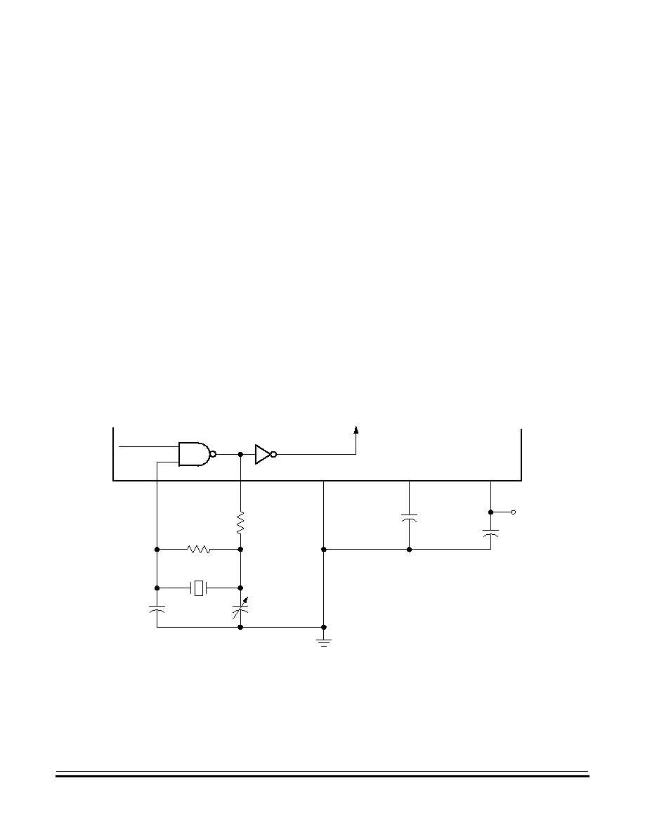
Clock Generator Module (CGM)
Functional Description
MC68HC(7)08KH12
--
Rev. 1.0
Advance Information
MOTOROLA
Clock Generator Module (CGM)
97
∑
Tuning capacitor, C
2
(can also be a fixed capacitor)
∑
Feedback resistor, R
B
∑
Series resistor, R
S
(optional)
The series resistor (R
S
) is included in the diagram to follow strict Pierce
oscillator guidelines and may not be required for all ranges of operation,
especially with high frequency crystals. Refer to the crystal
manufacturer's data for more information.
Figure 8-2
also shows the external components for the PLL:
∑
Bypass capacitor, C
BYP
∑
Filter capacitor, C
F
Routing should be done with great care to minimize signal cross talk and
noise.
See
Section 17. Preliminary Electrical Specifications
for capacitor
and resistor values.
Figure 8-2. CGM External Connections
SIMOSCEN
CGMXCLK
R
B
X
1
*R
S
can be zero (shorted) when used with higher-frequency crystals. Refer to manufacturer's data.
OSC1
OSC2
V
SSA
CGMXFC
V
DDA
V
DD
C
BYP
R
S
*
C
1
C
2
C
F

Clock Generator Module (CGM)
Advance Information
MC68HC(7)08KH12
--
Rev. 1.0
98
Clock Generator Module (CGM)
MOTOROLA
8.5 I/O Signals
The following paragraphs describe the CGM I/O signals.
8.5.1 Crystal Amplifier Input Pin (OSC1)
The OSC1 pin is an input to the crystal oscillator amplifier.
8.5.2 Crystal Amplifier Output Pin (OSC2)
The OSC2 pin is the output of the crystal oscillator inverting amplifier.
8.5.3 External Filter Capacitor Pin (CGMXFC)
The CGMXFC pin is required by the loop filter to filter out phase
corrections. A small external capacitor is connected to this pin.
NOTE:
To prevent noise problems, C
F
should be placed as close to the
CGMXFC pin as possible, with minimum routing distances and no
routing of other signals across the C
F
connection.
8.5.4 PLL Analog Power Pin (V
DDA
)
V
DDA
is a power pin used by the analog portions of the PLL. Connect the
V
DDA
pin to the same voltage potential as the V
DD
pin.
NOTE:
Route V
DDA
carefully for maximum noise immunity and place bypass
capacitors as close as possible to the package.
8.5.5 PLL Analog Ground Pin (V
SSA
)
V
SSA
is a ground pin used by the analog portions of the PLL. Connect
the V
SSA
pin to the same voltage potential as the V
SS
pin.
NOTE:
Route V
SSA
carefully for maximum noise immunity and place bypass
capacitors as close as possible to the package.

Clock Generator Module (CGM)
I/O Signals
MC68HC(7)08KH12
--
Rev. 1.0
Advance Information
MOTOROLA
Clock Generator Module (CGM)
99
8.5.6 Buffered Crystal Clock Output (CGMVOUT)
CGMVOUT buffers the OSC1 clock for external use.
8.5.7 CGMVSEL
CGMVSEL must be tied low or floated.
8.5.8 Oscillator Enable Signal (SIMOSCEN)
The SIMOSCEN signal comes from the system integration module (SIM)
and enables the oscillator and PLL.
8.5.9 Crystal Output Frequency Signal (CGMXCLK)
CGMXCLK is the crystal oscillator output signal. It runs at the full speed
of the crystal (f
XCLK
) and comes directly from the crystal oscillator circuit.
Figure 8-2
shows only the logical relation of CGMXCLK to OSC1 and
OSC2 and may not represent the actual circuitry. The duty cycle of
CGMXCLK is unknown and may depend on the crystal and other
external factors. Also, the frequency and amplitude of CGMXCLK can be
unstable at startup.
8.5.10 CGM Base Clock Output (CGMOUT)
CGMOUT is the clock output of the CGM. This signal goes to the SIM,
which generates the MCU clocks. CGMOUT is a 50 percent duty cycle
clock running at twice the bus frequency. CGMOUT is software
programmable to be either the oscillator output, CGMXCLK, divided by
two or the VCO clock, CGMVCLK, divided by two.
8.5.11 CGM CPU Interrupt (CGMINT)
CGMINT is the interrupt signal generated by the PLL lock detector.

Clock Generator Module (CGM)
Advance Information
MC68HC(7)08KH12
--
Rev. 1.0
100
Clock Generator Module (CGM)
MOTOROLA
8.6 CGM Registers
These registers control and monitor operation of the CGM:
∑
PLL control register (PCTL) (See
8.6.1 PLL Control Register
(PCTL)
.)
∑
PLL bandwidth control register (PBWC) (See
8.6.2 PLL
Bandwidth Control Register (PBWC)
.)
∑
PLL multiplier select registers (PMSH:PMSL) (See
8.6.3 PLL
Multiplier Select Registers (PMSH:PMSL)
.)
∑
PLL reference divider select register (PRDS) (See
8.6.4 PLL
Reference Divider Select Register (PRDS)
.)
Table 8-2
is a summary of the CGM registers.
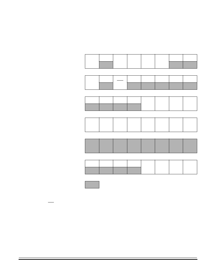
Clock Generator Module (CGM)
CGM Registers
MC68HC(7)08KH12
--
Rev. 1.0
Advance Information
MOTOROLA
Clock Generator Module (CGM)
101
Table 8-2. CGM I/O Register Summary
Addr.
Register Name
Bit 7
6
5
4
3
2
1
Bit 0
$003A
PLL Control Register
(PCTL)
Read:
PLLIE
PLLF
PLLON
BCS
PRE1
PRE2
0
0
Write:
Reset:
0
0
1
0
1
0
0
0
$003B
PLL Bandwidth Control
Register
(PBWC)
Read:
AUTO
LOCK
ACQ
0
0
0
0
0
Write:
Reset:
0
0
0
0
0
0
0
0
$003C
PLL Multiplier Select
Register High
(PMSH)
Read:
0
0
0
0
MUL11
MUL10
MUL9
MUL8
Write:
Reset:
0
0
0
0
0
0
0
0
$003D
PLL Multiplier Select
Register Low
(PMSL)
Read:
MUL7
MUL6
MUL5
MUL4
MUL3
MUL2
MUL1
MUL0
Write:
Reset:
0
0
0
0
0
0
1
0
$003E
Unimplemented
Read:
Write:
Reset:
$003F
PLL Reference Divider
Select Register
(PRDS)
Read:
0
0
0
0
RDS3
RDS2
RDS1
RDS0
Write:
Reset:
0
0
0
0
0
0
0
1
= Unimplemented
NOTES:
1. When AUTO = 0, PLLIE is forced clear and is read-only.
2. When AUTO = 0, PLLF and LOCK read as clear.
3. When AUTO = 1, ACQ is read-only.
4. When PLLON = 0 or VRS7:VRS0 = $0, BCS is forced clear and is read-only.
5. When PLLON = 1, the PLL programming register is read-only.
6. When BCS = 1, PLLON is forced set and is read-only.
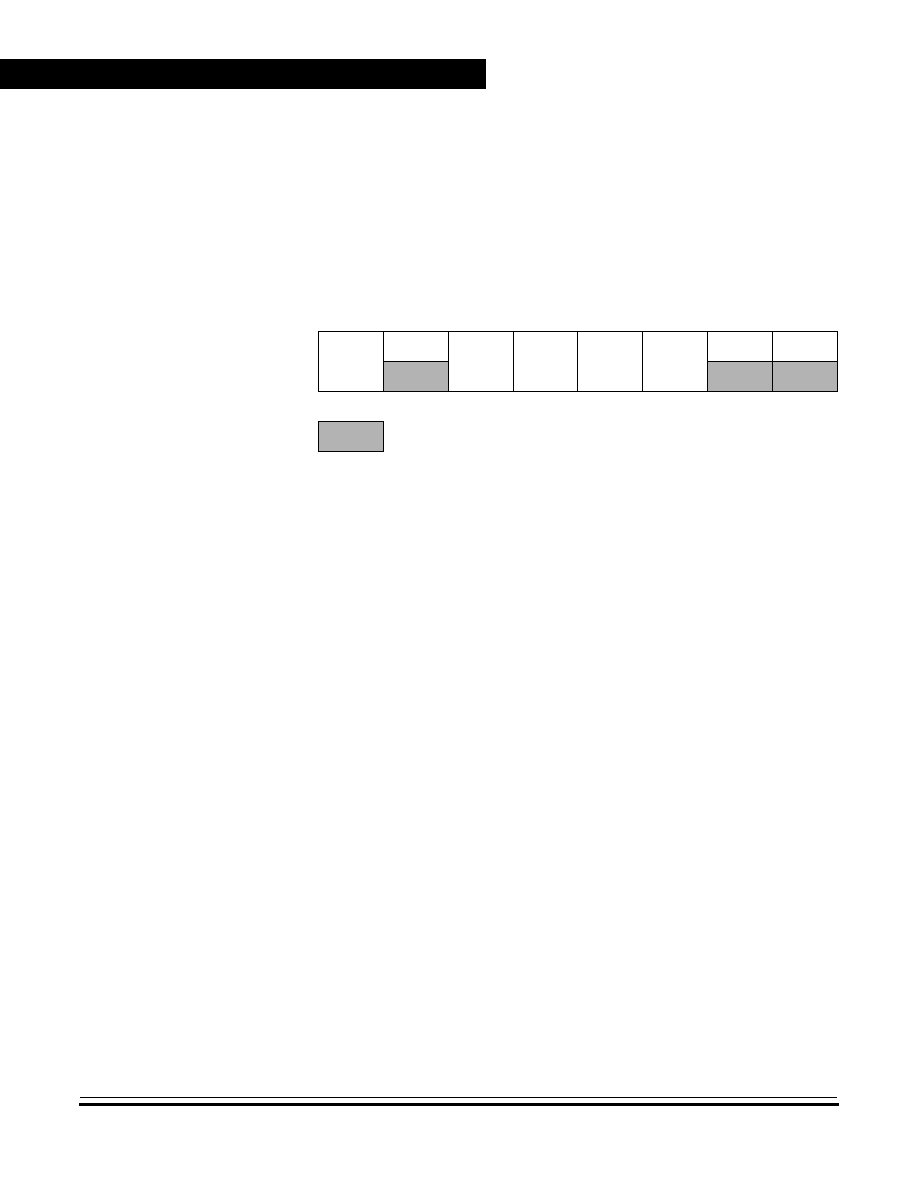
Clock Generator Module (CGM)
Advance Information
MC68HC(7)08KH12
--
Rev. 1.0
102
Clock Generator Module (CGM)
MOTOROLA
8.6.1 PLL Control Register (PCTL)
The PLL control register contains the interrupt enable and flag bits, the
on/off switch, the base clock selector bit, the prescaler bits, and the VCO
power of two range selector bits.
PLLIE -- PLL Interrupt Enable Bit
This read/write bit enables the PLL to generate an interrupt request
when the LOCK bit toggles, setting the PLL flag, PLLF. When the
AUTO bit in the PLL bandwidth control register (PBWC) is clear,
PLLIE cannot be written and reads as logic zero. Reset clears the
PLLIE bit.
1 = PLL interrupts enabled
0 = PLL interrupts disabled
PLLF -- PLL Interrupt Flag Bit
This read-only bit is set whenever the LOCK bit toggles. PLLF
generates an interrupt request if the PLLIE bit also is set. PLLF
always reads as logic zero when the AUTO bit in the PLL bandwidth
control register (PBWC) is clear. Clear the PLLF bit by reading the
PLL control register. Reset clears the PLLF bit.
1 = Change in lock condition
0 = No change in lock condition
NOTE:
Do not inadvertently clear the PLLF bit. Any read or read-modify-write
operation on the PLL control register clears the PLLF bit.
Address:
$003A
Bit 7
6
5
4
3
2
1
Bit 0
Read:
PLLIE
PLLF
PLLON
BCS
PRE1
PRE2
0
0
Write:
Reset:
0
0
1
0
1
0
0
0
= Unimplemented
Figure 8-3. PLL Control Register (PCTL)

Clock Generator Module (CGM)
CGM Registers
MC68HC(7)08KH12
--
Rev. 1.0
Advance Information
MOTOROLA
Clock Generator Module (CGM)
103
PLLON -- PLL On Bit
This read/write bit activates the PLL and enables the VCO clock,
CGMVCLK. PLLON cannot be cleared if the VCO clock is driving the
base clock, CGMOUT (BCS = 1). (See
8.4.8 Base Clock Selector
Circuit
.) Reset sets this bit so that the loop can stabilize as the MCU
is powering up.
1 = PLL on
0 = PLL off
BCS -- Base Clock Select Bit
This read/write bit selects either the crystal oscillator clock
(CGMXCLK) or the VCO clocks (CGMPCLK and CGMVCLK) to use
as base clocks for the MCU.
BCS cannot be set while the PLLON bit is clear. After toggling BCS,
it may take up to three CGMXCLK and three CGMPCLK cycles to
complete the transition from one source clock to the other. During the
transition, CGMOUT is held in stasis. (See
8.4.8 Base Clock
Selector Circuit
.) Reset clears the BCS bit.
1 = Selects the VCO clocks for the base clock.
CGMPCLK divided by two drives CGMOUT,
CGMVCLK (48MHz) drives USBCLK
0 = Selects the crystal oscillator clock for the base clock.
CGMXCLK divided by two drives CGMOUT,
CGMXCLK drives USBCLK
NOTE:
PLLON and BCS have built-in protection that prevents the base clock
selector circuit from selecting the VCO clock as the source of the base
clock if the PLL is off. Therefore, PLLON cannot be cleared when BCS
is set, and BCS cannot be set when PLLON is clear. If the PLL is off
(PLLON = 0), selecting CGMPCLK/CGMVCLK requires two writes to the
PLL control register. (See
8.4.8 Base Clock Selector Circuit
.)
PRE1 and PRE0 -- Prescaler program bits
These read/write bits control a prescaler that selects the prescaler
power-of-two multiplier P. (See
8.4.3 PLL Circuits
and
8.4.6
Programming the PLL
.) PRE1:PRE0 cannot be written when the
PLLON bit is set. Reset clears these bits.
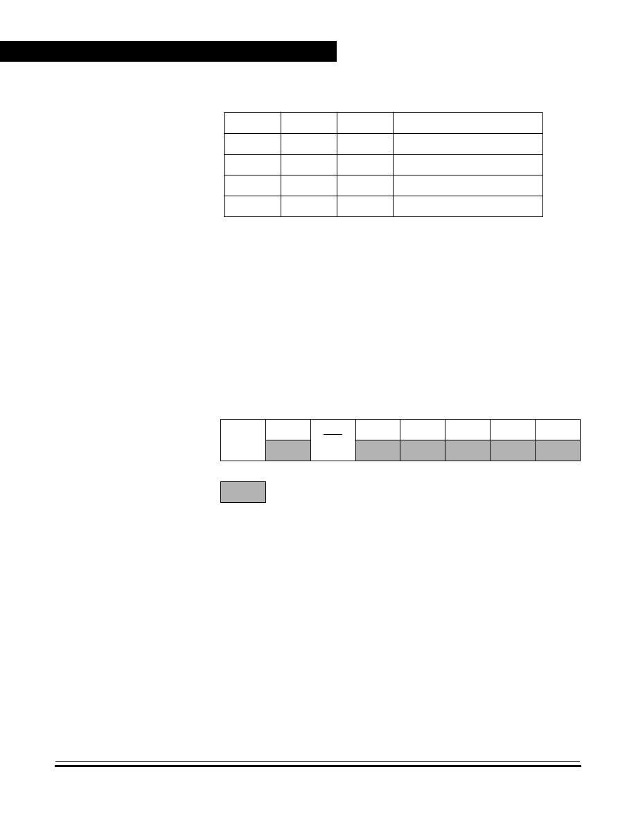
Clock Generator Module (CGM)
Advance Information
MC68HC(7)08KH12
--
Rev. 1.0
104
Clock Generator Module (CGM)
MOTOROLA
8.6.2 PLL Bandwidth Control Register (PBWC)
The PLL bandwidth control register:
∑
Indicates when the PLL is locked
∑
In automatic bandwidth control mode, indicates when the PLL is in
acquisition or tracking mode
AUTO -- Automatic Bandwidth Control Bit
This read/write bit selects automatic or manual bandwidth control.
Since this CGM is optimized a frequency output of 48MHz for the USB
module, automatic control should be set. Reset clears the AUTO bit.
1 = Automatic bandwidth control (recommended)
0 = Manual bandwidth control
LOCK -- Lock Indicator Bit
When the AUTO bit is set, LOCK is a read-only bit that becomes set
when the VCO clock, CGMVCLK, is locked (running at the
programmed frequency). When the AUTO bit is clear, LOCK reads as
Table 8-3. PRE[1:0] Programming
PRE1
PRE0
P
Prescaler Multiplier
0
0
0
1
0
1
1
2
1
0
2
4
1
1
3
8
Address:
$003B
Bit 7
6
5
4
3
2
1
Bit 0
Read:
AUTO
LOCK
ACQ
0
0
0
0
0
Write:
Reset:
0
0
0
0
0
0
0
0
= Unimplemented
Figure 8-4. PLL Bandwidth Control Register (PBWC)
Clock Generator Module (CGM)
CGM Registers
MC68HC(7)08KH12
--
Rev. 1.0
Advance Information
MOTOROLA
Clock Generator Module (CGM)
105
logic zero and has no meaning. The write one function of this bit is
reserved for test, so this bit must
always be written a zero. Reset
clears the LOCK bit.
1 = VCO frequency correct or locked
0 = VCO frequency incorrect or unlocked
ACQ -- Acquisition Mode Bit
When the AUTO bit is set, ACQ is a read-only bit that indicates
whether the PLL is in acquisition mode or tracking mode. When the
AUTO bit is clear, ACQ is a read/write bit that controls whether the
PLL is in acquisition or tracking mode.
In automatic bandwidth control mode (AUTO = 1), the last-written
value from manual operation is stored in a temporary location and is
recovered when manual operation resumes. Reset clears this bit,
enabling acquisition mode.
1 = Tracking mode
0 = Acquisition mode
8.6.3 PLL Multiplier Select Registers (PMSH:PMSL)
The PLL multiplier select registers contain the programming information
for the modulo feedback divider.
Address:
$003C
PMSH
Bit 7
6
5
4
3
2
1
Bit 0
Read:
0
0
0
0
MUL11
MUL10
MUL9
MUL8
Write:
Reset:
0
0
0
0
0
0
0
0
Address:
$003D
PMSL
Read:
MUL7
MUL6
MUL5
MUL4
MUL3
MUL2
MUL1
MUL0
Write:
Reset:
0
0
0
0
0
0
1
0
= Unimplemented
Figure 8-5. PLL Multiplier Select Registers (PMSH:PMSL)
Clock Generator Module (CGM)
Advance Information
MC68HC(7)08KH12
--
Rev. 1.0
106
Clock Generator Module (CGM)
MOTOROLA
MUL[11:0] -- Multiplier select bits
These read/write bits control the modulo feedback divider that selects
the VCO frequency multiplier N. (See
8.4.3 PLL Circuits
and
8.4.6
Programming the PLL
.) MUL[11:0] cannot be written when the
PLLON bit in the PCTL is set. A value of $0000 in the multiplier select
registers configures the modulo feedback divider the same as a value
of $0001. Reset initializes the registers to $002 for a default multiply
value of 2.
NOTE:
The multiplier select bits have built-in protection such that they cannot
be written when the PLL is on (PLLON = 1).
8.6.4 PLL Reference Divider Select Register (PRDS)
The PLL reference divider select register contains the programming
information for the modulo reference divider.
RDS[3:0] -- Reference Divider Select Bits
These read/write bits control the modulo reference divider that selects
the reference division factor R. (See
8.4.3 PLL Circuits
and
8.4.6
Programming the PLL
.) RDS[7:0] cannot be written when the
PLLON bit in the PCTL is set. A value of $00 in the reference divider
select register configures the reference divider the same as a value of
$01. (See
8.4.7 Special Programming Exceptions
.) Reset
initializes the register to $01 for a default divide value of 1.
NOTE:
The reference divider select bits have built-in protection such that they
cannot be written when the PLL is on (PLLON = 1).
Address:
$003F
Bit 7
6
5
4
3
2
1
Bit 0
Read:
0
0
0
0
RDS3
RDS2
RDS1
RDS0
Write:
Reset:
0
0
0
0
0
0
0
1
= Unimplemented
Figure 8-6. PLL Reference Divider Select Register (PRDS)

Clock Generator Module (CGM)
Interrupts
MC68HC(7)08KH12
--
Rev. 1.0
Advance Information
MOTOROLA
Clock Generator Module (CGM)
107
8.7 Interrupts
When the AUTO bit is set in the PLL bandwidth control register (PBWC),
the PLL can generate a CPU interrupt request every time the LOCK bit
changes state. The PLLIE bit in the PLL control register (PCTL) enables
CPU interrupts from the PLL. PLLF, the interrupt flag in the PCTL,
becomes set whether interrupts are enabled or not. When the AUTO bit
is clear, CPU interrupts from the PLL are disabled and PLLF reads as
logic zero.
Software should read the LOCK bit after a PLL interrupt request to see
if the request was due to an entry into lock or an exit from lock. When the
PLL enters lock, the VCO clock, CGMPCLK, divided by two can be
selected as the CGMOUT source by setting BCS in the PCTL. When the
PLL exits lock, the VCO clock frequency is corrupt, and appropriate
precautions should be taken. If the application is not frequency sensitive,
interrupts should be disabled to prevent PLL interrupt service routines
from impeding software performance or from exceeding stack
limitations.
NOTE:
Software can select the CGMPCLK divided by two as the CGMOUT
source even if the PLL is not locked (LOCK = 0). Therefore, software
should make sure the PLL is locked before setting the BCS bit.
8.8 Special Modes
The WAIT instruction puts the MCU in low-power-consumption standby
modes.
8.8.1 Wait Mode
The WAIT instruction does not affect the CGM. Before entering wait
mode, software can disengage and turn off the PLL by clearing the BCS
and PLLON bits in the PLL control register (PCTL) to save power. Less
power-sensitive applications can disengage the PLL without turning it
off, so that the PLL clock is immediately available at WAIT exit. This
would also be the case when the PLL is to wake the MCU from wait
mode, such as when the PLL is first enabled and waiting for LOCK, or
LOCK is lost.

Clock Generator Module (CGM)
Advance Information
MC68HC(7)08KH12
--
Rev. 1.0
108
Clock Generator Module (CGM)
MOTOROLA
8.8.2 CGM During Break Interrupts
The system integration module (SIM) controls whether status bits in
other modules can be cleared during the break state. The BCFE bit in
the SIM break flag control register (SBFCR) enables software to clear
status bits during the break state. (See
7.8.3 Break Flag Control
Register (BFCR)
.)
To allow software to clear status bits during a break interrupt, write a
logic one to the BCFE bit. If a status bit is cleared during the break state,
it remains cleared when the MCU exits the break state.
To protect the PLLF bit during the break state, write a logic zero to the
BCFE bit. With BCFE at logic zero (its default state), software can read
and write the PLL control register during the break state without affecting
the PLLF bit.
8.9 Acquisition/Lock Time Specifications
The acquisition and lock times of the PLL are, in many applications, the
most critical PLL design parameters. Proper design and use of the PLL
ensures the highest stability and lowest acquisition/lock times.
8.9.1 Acquisition/Lock Time Definitions
Typical control systems refer to the acquisition time or lock time as the
reaction time, within specified tolerances, of the system to a step input.
In a PLL, the step input occurs when the PLL is turned on or when it
suffers a noise hit. The tolerance is usually specified as a percent of the
step input or when the output settles to the desired value plus or minus
a percent of the frequency change. Therefore, the reaction time is
constant in this definition, regardless of the size of the step input. For
example, consider a system with a 5 percent acquisition time tolerance.
If a command instructs the system to change from 0 Hz to 1 MHz, the
acquisition time is the time taken for the frequency to reach
1 MHz
±
50 kHz. Fifty kHz = 5% of the 1 MHz step input. If the system is
operating at 1 MHz and suffers a ≠100 kHz noise hit, the acquisition time
is the time taken to return from 900 kHz to 1 MHz
±
5 kHz.
Five kHz = 5 percent of the 100-kHz step input.

Clock Generator Module (CGM)
Acquisition/Lock Time Specifications
MC68HC(7)08KH12
--
Rev. 1.0
Advance Information
MOTOROLA
Clock Generator Module (CGM)
109
Other systems refer to acquisition and lock times as the time the system
takes to reduce the error between the actual output and the desired
output to within specified tolerances. Therefore, the acquisition or lock
time varies according to the original error in the output. Minor errors may
not even be registered. Typical PLL applications prefer to use this
definition because the system requires the output frequency to be within
a certain tolerance of the desired frequency regardless of the size of the
initial error.
The discrepancy in these definitions makes it difficult to specify an
acquisition or lock time for a typical PLL. Therefore, the definitions for
acquisition and lock times for this module are:
∑
Acquisition time, t
ACQ
, is the time the PLL takes to reduce the error
between the actual output frequency and the desired output
frequency to less than the tracking mode entry tolerance,
TRK
.
Acquisition time is based on an initial frequency error,
(f
DES
≠ f
ORIG
)/f
DES
, of not more than
±
100 percent. In automatic
bandwidth control mode (See
8.4.5 Manual and Automatic PLL
Bandwidth Modes
.), acquisition time expires when the ACQ bit
becomes set in the PLL bandwidth control register (PBWC).
∑
Lock time, t
LOCK
, is the time the PLL takes to reduce the error
between the actual output frequency and the desired output
frequency to less than the lock mode entry tolerance,
LOCK
. Lock
time is based on an initial frequency error, (f
DES
≠ f
ORIG
)/f
DES
, of not
more than
±
100 percent. In automatic bandwidth control mode,
lock time expires when the LOCK bit becomes set in the PLL
bandwidth control register (PBWC). (See
8.4.5 Manual and
Automatic PLL Bandwidth Modes
.)
Obviously, the acquisition and lock times can vary according to how
large the frequency error is and may be shorter or longer in many cases.
8.9.2 Parametric Influences on Reaction Time
Acquisition and lock times are designed to be as short as possible while
still providing the highest possible stability. These reaction times are not
constant, however. Many factors directly and indirectly affect the
acquisition time.

Clock Generator Module (CGM)
Advance Information
MC68HC(7)08KH12
--
Rev. 1.0
110
Clock Generator Module (CGM)
MOTOROLA
The most critical parameter which affects the reaction times of the PLL
is the reference frequency, f
RDV
. This frequency is the input to the phase
detector and controls how often the PLL makes corrections. For stability,
the corrections must be small compared to the desired frequency, so
several corrections are required to reduce the frequency error.
Therefore, the slower the reference the longer it takes to make these
corrections. This parameter is under user control via the choice of crystal
frequency f
XCLK
and the R value programmed in the reference divider.
(See
8.4.3 PLL Circuits
,
8.4.6 Programming the PLL
, and
8.6.4
PLL Reference Divider Select Register (PRDS)
.)
Another critical parameter is the external filter capacitor. The PLL
modifies the voltage on the VCO by adding or subtracting charge from
this capacitor. Therefore, the rate at which the voltage changes for a
given frequency error (thus change in charge) is proportional to the
capacitor size. The size of the capacitor also is related to the stability of
the PLL. If the capacitor is too small, the PLL cannot make small enough
adjustments to the voltage and the system cannot lock. If the capacitor
is too large, the PLL may not be able to adjust the voltage in a
reasonable time. (See
8.9.3 Choosing a Filter Capacitor
.)
Also important is the operating voltage potential applied to V
DDA
. The
power supply potential alters the characteristics of the PLL. A fixed value
is best. Variable supplies, such as batteries, are acceptable if they vary
within a known range at very slow speeds. Noise on the power supply is
not acceptable, because it causes small frequency errors which
continually change the acquisition time of the PLL.
Temperature and processing also can affect acquisition time because
the electrical characteristics of the PLL change. The part operates as
specified as long as these influences stay within the specified limits.
External factors, however, can cause drastic changes in the operation of
the PLL. These factors include noise injected into the PLL through the
filter capacitor, filter capacitor leakage, stray impedances on the circuit
board, and even humidity or circuit board contamination.

Clock Generator Module (CGM)
Acquisition/Lock Time Specifications
MC68HC(7)08KH12
--
Rev. 1.0
Advance Information
MOTOROLA
Clock Generator Module (CGM)
111
8.9.3 Choosing a Filter Capacitor
As described in
8.9.2 Parametric Influences on Reaction Time
, the
external filter capacitor, C
F
, is critical to the stability and reaction time of
the PLL. The PLL is also dependent on reference frequency and supply
voltage. The value of the capacitor must, therefore, be chosen with
supply potential and reference frequency in mind. For proper operation,
the external filter capacitor must be chosen according to this equation:
For the value of V
DDA
, choose the voltage potential at which the MCU is
operating. If the power supply is variable, choose a value near the
middle of the range of possible supply values.
This equation does not always yield a commonly available capacitor
size, so round to the nearest available size. If the value is between two
different sizes, choose the higher value for better stability. Choosing the
lower size may seem attractive for acquisition time improvement, but the
PLL may become unstable. Also, always choose a capacitor with a tight
tolerance (
±
20 percent or better) and low dissipation.
8.9.4 Reaction Time Calculation
The actual acquisition and lock times can be calculated using the
equations below. These equations yield nominal values under the
following conditions:
∑
Correct selection of filter capacitor, C
F
(See
8.9.3 Choosing a
Filter Capacitor
.)
∑
Room temperature operation
∑
Negligible external leakage on CGMXFC
∑
Negligible noise
The K factor in the equations is derived from internal PLL parameters.
K
ACQ
is the K factor when the PLL is configured in acquisition mode, and
K
TRK
is the K factor when the PLL is configured in tracking mode. (See
8.4.4 Acquisition and Tracking Modes
.) Reaction time is based on
C
F
C
FACT
V
DDA
f
RDV
-------------
=

Clock Generator Module (CGM)
Advance Information
MC68HC(7)08KH12
--
Rev. 1.0
112
Clock Generator Module (CGM)
MOTOROLA
an initial frequency error, (f
DES
≠ f
ORIG
)/f
DES
, of not more than
±
100
percent.
NOTE:
The inverse proportionality between the lock time and the reference
frequency.
In automatic bandwidth control mode, the acquisition and lock times are
quantized into units based on the reference frequency. (See
8.4.5
Manual and Automatic PLL Bandwidth Modes
.) A certain number of
clock cycles, n
ACQ
, is required to ascertain that the PLL is within the
tracking mode entry tolerance,
TRK
, before exiting acquisition mode. A
certain number of clock cycles, n
TRK
, is required to ascertain that the PLL
is within the lock mode entry tolerance,
LOCK
. Therefore, the acquisition
time, t
ACQ
, is an integer multiple of n
ACQ
/f
RDV
, and the acquisition to lock
time, t
AL
, is an integer multiple of n
TRK
/f
RDV
.
In manual mode, it is usually necessary to wait considerably longer than
t
LOCKMAX
before selecting the PLL clock (See
8.4.8 Base Clock
Selector Circuit
.), because the factors described in
8.9.2 Parametric
Influences on Reaction Time
may slow the lock time considerably.
Automatic bandwidth mode is recommended for most users.
t
ACQ
V
DDA
f
RDV
-------------
8
K
ACQ
-------------
=
t
AL
V
DDA
f
RDV
-------------
4
K
TRK
------------
=
t
LOCKMAX
t
ACQ
t
AL
256t
VRDV
+
+
=

MC68HC(7)08KH12
--
Rev. 1.0
Advance Information
MOTOROLA
Universal Serial Bus Module (USB)
113
Advance Information -- MC68HC(7)08KH12
Section 9. Universal Serial Bus Module (USB)
9.1 Contents
9.2
Features . . . . . . . . . . . . . . . . . . . . . . . . . . . . . . . . . . . . . . . . . 114
9.3
Overview. . . . . . . . . . . . . . . . . . . . . . . . . . . . . . . . . . . . . . . . . 115
9.4
I/O Register Description of the HUB function . . . . . . . . . . . . . 116
9.4.1
USB HUB Root Port Control Register (HRPCR) . . . . . . . . 120
9.4.2
USB HUB Downstream Port Control Register
(HDP1CR-HDP4CR) . . . . . . . . . . . . . . . . . . . . . . . . . . 121
9.4.3
USB SIE Timing Interrupt Register (SIETIR). . . . . . . . . . . 123
9.4.4
USB SIE Timing Status Register (SIETSR) . . . . . . . . . . . 125
9.4.5
USB HUB Address Register (HADDR) . . . . . . . . . . . . . . . 127
9.4.6
USB HUB Interrupt Register 0 (HIR0) . . . . . . . . . . . . . . . . 128
9.4.7
USB HUB Control Register 0 (HCR0) . . . . . . . . . . . . . . . . 129
9.4.8
USB HUB Endpoint1 Control & Data Register (HCDR) . . 131
9.4.9
USB HUB Status Register (HSR) . . . . . . . . . . . . . . . . . . . 132
9.4.10
USB HUB Endpoint 0 Data Registers 0-7
(HE0D0-HE0D7). . . . . . . . . . . . . . . . . . . . . . . . . . . . . . 134
9.5
I/O Register Description of the Embedded Device Function . 134
9.5.1
USB Embedded Device Address Register (DADDR) . . . . 138
9.5.2
USB Embedded Device Interrupt Register 0 (DIR0) . . . . . 138
9.5.3
USB Embedded Device Interrupt Register 1 (DIR1) . . . . . 140
9.5.4
USB Embedded Device Control Register 0 (DCR0) . . . . . 141
9.5.5
USB Embedded Device Control Register 1 (DCR1) . . . . . 143
9.5.6
USB Embedded Device Status Register (DSR) . . . . . . . . 144
9.5.7
USB Embedded Device Control Register 2 (DCR2) . . . . . 146
9.5.8
USB Embedded Device Endpoint 0 Data Registers
(DE0D0-DE0D7). . . . . . . . . . . . . . . . . . . . . . . . . . . . . . 147
9.5.9
USB Embedded Device Endpoint 1/2 Data Registers
(DE1D0-DE1D7). . . . . . . . . . . . . . . . . . . . . . . . . . . . . . 148

Universal Serial Bus Module (USB)
Advance Information
MC68HC(7)08KH12
--
Rev. 1.0
114
Universal Serial Bus Module (USB)
MOTOROLA
9.2 Features
Features of the general USB Module include the following:
∑
Integrated 3.3 Volt Regulator with 3.3V Output Pin REGOUT
∑
Integrated USB transceiver supporting both full speed and low
speed functions
∑
USB Data Control Logic
≠
Packet decoding/generation
≠
CRC generation and checking
≠
NRZI encoding/decoding
≠
Bit stuffing/de-stuffing
∑
USB reset support
∑
Suspend and resume operations
≠
Remote Wakeup support
∑
STALL, NAK, and ACK handshake generation
Features of the HUB function include the following:
∑
HUB Control Endpoint 0
≠
8-byte transmit buffer
≠
8-byte receive buffer
∑
HUB Interrupt Endpoint 1
≠
1-byte transmit buffer
∑
USB interrupts
≠
transaction interrupt driven
≠
Start of Frame interrupt
≠
EOF2 interrupt
≠
End of Packet interrupt
≠
Signal transition interrupt
≠
Frame timer locked interrupt
∑
HUB repeater and controller function
≠
downstream and upstream connectivity
≠
bus state evaluation
≠
selective reset, suspend and resume
≠
fault condition hardware detection

Universal Serial Bus Module (USB)
Overview
MC68HC(7)08KH12
--
Rev. 1.0
Advance Information
MOTOROLA
Universal Serial Bus Module (USB)
115
Features of the embedded device function include the following:
∑
Device Control Endpoint 0 and Interrupt Endpoints 1 and 2
≠
8-byte transmit buffer
≠
8-byte receive buffer
∑
Device Interrupt Endpoints 1 and 2
≠
8-byte transmit buffer
∑
USB generated interrupts
≠
transaction interrupt driven
9.3 Overview
This section provides an overview of the Universal Serial Bus (USB)
module developed for the MC68HC(7)08KH12. This USB module is
designed to serve as a compound device, and operates from a reference
frequency of 48MHz, derived from the CGM
(see Section 8. Clock
Generator Module (CGM)
). An embedded full speed device function is
combined with a hub in a single USB module. For the hub sub-module,
five basic properties can be supported by the hardware or the software:
connectivity behavior, power management, device connect/disconnect
detection, bus fault detection and recovery, and full/low speed device
traffic control. Endpoint 0 of the hub sub-module functions as a
receive/transmit control endpoint. Endpoint 1 of the hub sub-module
functions as interrupt transfer to report the device change state. For the
embedded device sub-module, three types of USB data transfers are
supported: control, interrupt, and bulk (transmit only). Endpoint 0 of the
embedded device sub-module functions as a receive/transmit control
endpoint. Endpoints 1 and 2 of the embedded device sub-module can
function as interrupt or bulk, but only in the transmit direction.
A block diagram of the USB module is shown
Figure 9-1
. The USB
module manages communications between the host and the USB
function. The module is partitioned into eight functional blocks. These
blocks consist of a 3.3 volt regulator, a dual function transceiver, the hub
repeater function, the SIE (Serial Interface Engine), the frame counter
logic, the hub control logic, the embedded device control logic, and the
endpoint registers.
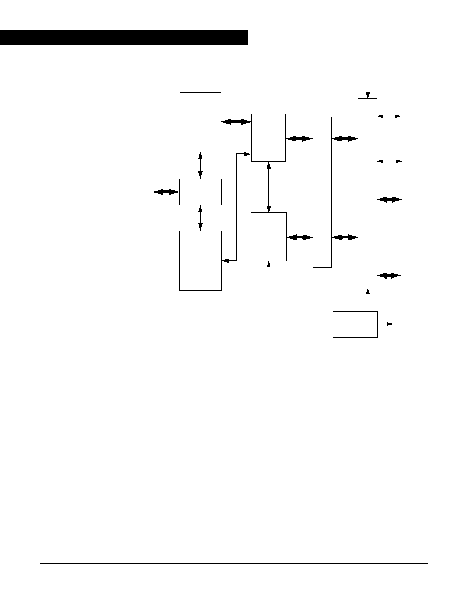
Universal Serial Bus Module (USB)
Advance Information
MC68HC(7)08KH12
--
Rev. 1.0
116
Universal Serial Bus Module (USB)
MOTOROLA
Figure 9-1. USB Block Diagram
9.4 I/O Register Description of the HUB function
The USB hub function provides a set of control/status registers and
sixteen data registers that provide storage for the buffering of data
between the USB hub function and the CPU. These registers are shown
in
Table 9-1
and
Table 9-2
.
D0+
D0≠
T
R
ANSCEIV
ER
3.3V OUT
CPU BUS
T
R
ANSCEIV
ER
D1+
:
D4+
D1≠
:
D4≠
R
OOR POR
T
DO
WNSTREAM POR
TS
HUB REPEA
TER
REGULATOR
SERIAL
FR
AME
COUNTER
ENGINE
HUB
CONTROL
LOGIC
REGISTERS
ENDPOINT 0 - 8/8 B (CONTROL)
ENDPOINT 1 - 1 B (INTERRUPT)
ENDPOINT 0 - 8/8 (CONTROL)
ENDPOINT 1/2 - 8 B (TRANSMIT ONLY, INTERRUPT/BULK)
12MHz
USBCLK (FROM CGM)
EMBEDDED DE
VICE
CONTROL
LOGIC
INTERF
A
C
E
48MHz
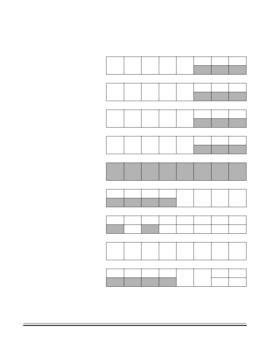
Universal Serial Bus Module (USB)
I/O Register Description of the HUB function
MC68HC(7)08KH12
--
Rev. 1.0
Advance Information
MOTOROLA
Universal Serial Bus Module (USB)
117
Table 9-1. HUB Control Register Summary
Addr.
Register Name
Bit 7
6
5
4
3
2
1
Bit 0
$0051
USB HUB Downstream Port 1
Control Register
(HDP1CR)
Read:
PEN1
LOWSP1
RST1
RESUM1
SUSP1
0
D1+
D1≠
Write:
Reset:
0
0
0
0
0
0
X
X
$0052
USB HUB Downstream Port 2
Control Register
(HDP2CR)
Read:
PEN2
LOWSP2
RST2
RESUM2
SUSP2
0
D2+
D2≠
Write:
Reset:
0
0
0
0
0
0
X
X
$0053
USB HUB Downstream Port 3
Control Register
(HDP3CR)
Read:
PEN3
LOWSP3
RST3
RESUM3
SUSP3
0
D3+
D3≠
Write:
Reset:
0
0
0
0
0
0
X
X
$0054
USB HUB Downstream Port 4
Control Register
(HDP4CR)
Read:
PEN4
LOWSP4
RST4
RESUM4
SUSP4
0
D4+
D4≠
Write:
Reset:
0
0
0
0
0
0
X
X
$0055
Unimplemented
Read:
Write:
Reset:
$0056
USB SIE Timing Interrupt
Register
(SIETIR)
Read:
SOFF
EOF2F
EOPF
TRANF
SOFIE
EOF2IE
EOPIE
TRANIE
Write:
Reset:
0
0
0
0
0
0
0
0
$0057
USB SIE Timing Status
Register
(SIETSR)
Read:
RSTF
0
LOCKF
0
0
0
0
0
Write:
RSTFR
LOCKFR SOFFR
EOF2FR
EOPFR TRANFR
Reset:
0**
0
0
0
0
0
0
0
$0058
USB HUB Address Register
(HADDR)
Read:
USBEN
ADD6
ADD5
ADD4
ADD3
ADD2
ADD1
ADD0
Write:
Reset:
0**
0
0
0
0
0
0
0
$0059
USB HUB Interrupt
Register 0
(HIR0)
Read:
TXDF
RXDF
0
0
TXDIE
RXDIE
0
0
Write:
TXDFR
RXDFR
Reset:
0
0
0
0
0
0
0
0
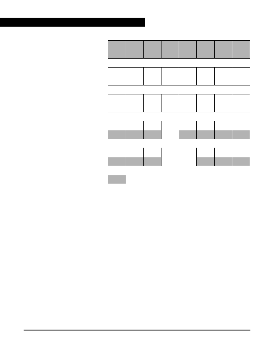
Universal Serial Bus Module (USB)
Advance Information
MC68HC(7)08KH12
--
Rev. 1.0
118
Universal Serial Bus Module (USB)
MOTOROLA
$005A
Unimplemented
Read:
Write:
Reset:
$005B
USB HUB Control
Register 0
(HCR0)
Read:
TSEQ
STALL0
TXE
RXE
TPSIZ3
TPSIZ2
TPSIZ1
TPSIZ0
Write:
Reset:
0
0
0
0
0
0
0
0
$005C
USB HUB Endpoint 1
Control and Data Register
(HCDR)
Read:
STALL1
PNEW
PCHG5
PCHG4
PCHG3
PCHG2
PCHG1
PCHG0
Write:
Reset:
0
0
0
0
0
0
0
0
$005D
USB HUB Status Register
(HSR)
Read:
RSEQ
SETUP
TX1ST
0
RPSIZ3
RPSIZ2
RPSIZ1
RPSIZ0
Write:
TX1STR
Reset:
X
X
0
0
X
X
X
X
$005E
USB HUB Root Port Control
Register
(HRPCR)
Read:
0
0
0
RESUM0
SUSPND
0
D0+
D0≠
Write:
Reset:
0
0
0
0
0
0
X
X
= Unimplemented
X = Indeterminate
0** = Reset by POR only
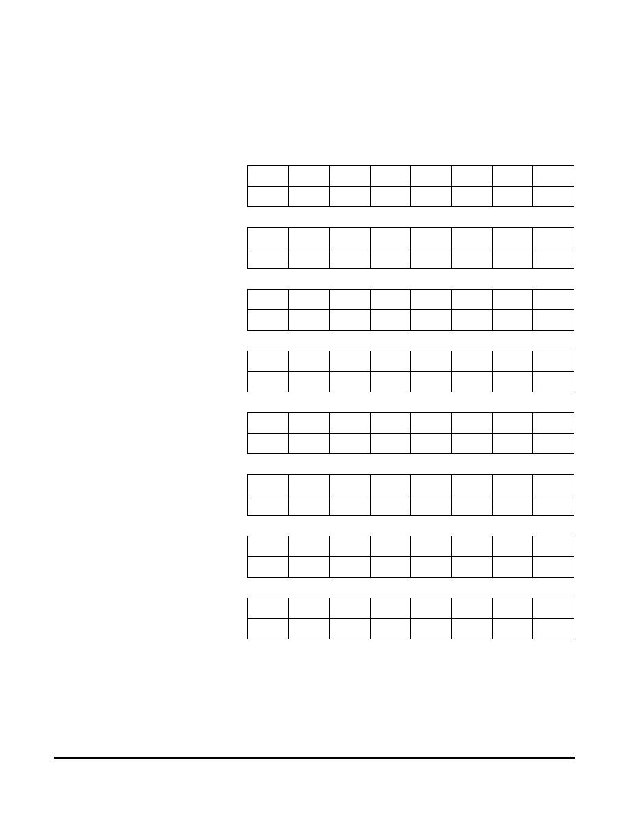
Universal Serial Bus Module (USB)
I/O Register Description of the HUB function
MC68HC(7)08KH12
--
Rev. 1.0
Advance Information
MOTOROLA
Universal Serial Bus Module (USB)
119
Table 9-2. HUB Data Register Summary
Addr.
Register Name
Bit 7
6
5
4
3
2
1
Bit 0
$0030
USB HUB Endpoint 0 Data
Register 0
(HE0D0)
Read: HE0R07 HE0R06 HE0R05 HE0R04 HE0R03 HE0R02 HE0R01 HE0R00
Write: HE0T07
HE0T06
HE0T05
HE0T04
HE0T03
HE0T02
HE0T01
HE0T00
Reset:
X
X
X
X
X
X
X
X
$0031
USB HUB Endpoint 0 Data
Register 1
(HE0D1)
Read: HE0R17 HE0R16 HE0R15 HE0R14 HE0R13 HE0R12 HE0R11 HE0R10
Write: HE0T17
HE0T16
HE0T15
HE0T14
HE0T13
HE0T12
HE0T11
HE0T10
Reset:
X
X
X
X
X
X
X
X
$0032
USB HUB Endpoint 0 Data
Register 2
(HE0D2)
Read: HE0R27 HE0R26 HE0R25 HE0R24 HE0R23 HE0R22 HE0R21 HE0R20
Write: HE0T27
HE0T26
HE0T25
HE0T24
HE0T23
HE0T22
HE0T21
HE0T20
Reset:
X
X
X
X
X
X
X
X
$0033
USB HUB Endpoint 0 Data
Register 3
(HE0D3)
Read: HE0R37 HE0R36 HE0R35 HE0R34 HE0R33 HE0R32 HE0R31 HE0R30
Write: HE0T37
HE0T36
HE0T35
HE0T34
HE0T33
HE0T32
HE0T31
HE0T30
Reset:
X
X
X
X
X
X
X
X
$0034
USB HUB Endpoint 0 Data
Register 4
(HE0D4)
Read: HE0R47 HE0R46 HE0R45 HE0R44 HE0R43 HE0R42 HE0R41 HE0R40
Write: HE0T47
HE0T46
HE0T45
HE0T44
HE0T43
HE0T42
HE0T41
HE0T40
Reset:
X
X
X
X
X
X
X
X
$0035
USB HUB Endpoint 0 Data
Register 5
(HE0D5)
Read: HE0R57 HE0R56 HE0R55 HE0R54 HE0R53 HE0R52 HE0R51 HE0R50
Write: HE0T57
HE0T56
HE0T55
HE0T54
HE0T53
HE0T52
HE0T51
HE0T50
Reset:
X
X
X
X
X
X
X
X
$0036
USB HUB Endpoint 0 Data
Register 6
(HE0D6)
Read: HE0R67 HE0R66 HE0R65 HE0R64 HE0R63 HE0R62 HE0R61 HE0R60
Write: HE0T67
HE0T66
HE0T65
HE0T64
HE0T63
HE0T62
HE0T61
HE0T60
Reset:
X
X
X
X
X
X
X
X
$0037
USB HUB Endpoint 0 Data
Register 7
(HE0D7)
Read: HE0R77 HE0R76 HE0R75 HE0R74 HE0R73 HE0R72 HE0R71 HE0R70
Write: HE0T77
HE0T76
HE0T75
HE0T74
HE0T73
HE0T72
HE0T71
HE0T70
Reset:
X
X
X
X
X
X
X
X
Universal Serial Bus Module (USB)
Advance Information
MC68HC(7)08KH12
--
Rev. 1.0
120
Universal Serial Bus Module (USB)
MOTOROLA
9.4.1 USB HUB Root Port Control Register (HRPCR)
RESUM0 -- Force Resume to the Root Port
This read/write bit forces a resume signal ("K" state) onto the USB
root port data lines to initiate a remote wakeup. Software should
control the timing of the forced resume to be between 10 ms and 15
ms. Reset clears this bit.
1 = Force root port data lines to "K" state
0 = Default
SUSPND -- USB Suspend Control Bit
To save power, this read/write bit should be set by the software if at
least 3ms constant idle state is detected on USB bus. Setting this bit
puts the transceiver and regulator into a power savings mode.
This bit also determines the latch scheme for the data lines of the root
port and the downstream port. When this bit is 1, the current state
shown on the data lines will be reflected to the data register (D+/D≠)
directly. When the bit is 0, the data registers are the latched state
sampled at the last EOF2 sample point. The hub repeater's function
is affected by this bit too. The upstream and downstream traffic will be
blocked if this bit is set to 1. When the global resume or the
downstream remote wakeup signal is found by the suspend hub,
software is responsible to propagate the traffic between the root port
and the enabled downstream port by setting the RESUMx control bit.
Reset clears this bit.
Address:
$005E
Bit 7
6
5
4
3
2
1
Bit 0
Read:
0
0
0
RESUM0 SUSPND
0
D0+
D0≠
Write:
Reset:
0
0
0
0
0
0
X
X
= Unimplemented
X = Indeterminate
Figure 9-2. USB HUB Root Port Control Register (HRPCR)
Universal Serial Bus Module (USB)
I/O Register Description of the HUB function
MC68HC(7)08KH12
--
Rev. 1.0
Advance Information
MOTOROLA
Universal Serial Bus Module (USB)
121
EOF2 is generated by KH12 every millisecond, if SOF is not detected
when three or more EOF2 has occurred, software can set the
SUSPND-bit and put KH12 into suspend mode.
D0+/D0≠ -- Root Port Differential Data
These read only bits are the differential data shown on the HUB root
ports. When the bit SUSPND is 0, the data is the latched state at the
last EOF2 sample point. When the bit SUSPND is 1, the data reflects
the current state on the data line while accessing this register.
9.4.2 USB HUB Downstream Port Control Register (HDP1CR-HDP4CR)
PEN1-PEN4 -- Downstream Port Enable Control Bit
This read/write bit determines whether the enabled or disabled state
should be assigned to the downstream port. Setting this bit 1 to
enable the port and clear the bit to disable the port. In the enabled
state a full-speed port propagates all downstream signaling, a low-
speed port propagates downstream low-speed packet traffic when
preceded by the preamble PID. An enabled port propagates all
upstream signaling including full speed and low speed packets. This
Address: $0051
Bit 7
6
5
4
3
2
1
Bit 0
Read:
PEN1
LOWSP1
RST1
RESUM1
SUSP1
0
D1+
D1≠
Write:
Reset:
0
0
0
0
0
0
X
X
Address: $0054
Read:
PEN4
LOWSP4
RST4
RESUM4
SUSP4
0
D4+
D4≠
Write:
Reset:
0
0
0
0
0
0
X
X
= Unimplemented
X = Indeterminate
Figure 9-3. USB HUB Downstream Port Control Registers
(HDP1CR-HDP4CR)

Universal Serial Bus Module (USB)
Advance Information
MC68HC(7)08KH12
--
Rev. 1.0
122
Universal Serial Bus Module (USB)
MOTOROLA
bit can be set to 1 by the host request only. It can be cleared either by
hardware when a fault condition was detected or by software through
the host request. Reset clears this bit.
1 = Downstream port is enabled
0 = Downstream port is disabled
LOWSP1-LOWSP4 -- Full Speed / Low Speed Port Control Bit
This read/write bit specifies the attached device in the downstream
port is low speed device or full speed device. Software is responsible
to detect the device attachment and whether a device is full or low
speed. Reset clears this bit.
1 = Downstream port is low speed
0 = Downstream port is full speed
NOTE:
after a port is enabled, HUB will automatically generate a low speed
keep awake signal to the port every millisecond.
RST1-RST4 -- Force Reset to the Downstream Port
This read/write bit forces a reset signal (SE0 state) onto the USB
downstream port data lines. This bit can be set by the host request
SetPortFeature (PORT_RESET) only. Software should control the
timing of the forced reset signaling downstream for at least 10 ms.
Reset clears this bit.
1 = Force downstream port data lines to SE0 state
0 = Default
RESUM1-RESUM4 -- Force Resume to the Downstream Port
This read/write bit forces a resume signal ("K" state) onto the USB
downstream port data lines. This bit is set to reflect the resume signal
when the software detects the remote resume signal on the data lines
of the selective suspend downstream port. Downstream selective
resume sequence to a port may also be initiated via the host request
ClearPortFeature (PORT_SUSPEND). Software should control the
timing of the forced resume signaling downstream for at least 20 ms.
To indicate the end of the resume, a low speed EOP signal will be
followed when this control bit changes from 1 to 0. Reset clears this
bit.
1 = Force downstream port data lines to "K" state
0 = Default

Universal Serial Bus Module (USB)
I/O Register Description of the HUB function
MC68HC(7)08KH12
--
Rev. 1.0
Advance Information
MOTOROLA
Universal Serial Bus Module (USB)
123
SUSP1-SUSP4 -- Downstream Port Selective Suspend Bit
This read/write bit forces the downstream port entering the selective
suspend mode. This bit can be set by the host request
SetPortFeature (PORT_SUSPEND) only. When this bit is set, the hub
prevents propagating any bus activity (except the port reset or port
resume request or the global reset signal) downstream, and the port
can only reflect upstream bus state changes via the endpoint 1 of the
hub. The blocking occurs at the next EOF2 point when this bit is set.
Reset clears this bit.
1 = Force downstream port enters the selective suspend mode
0 = Default
D1+/D1≠ to D4+/D4≠ -- Downstream Port Differential Data
These read only bits are the differential data shown on the HUB
downstream ports. When the bit SUSPND in the register HRPCR is 0,
the data is the latched state at the last EOF2 sample point. When the
bit SUSPND is 1, the data reflects the current state on the data line
while accessing this register.
9.4.3 USB SIE Timing Interrupt Register (SIETIR)
Address:
$0056
Bit 7
6
5
4
3
2
1
Bit 0
Read:
SOFF
EOF2F
EOPF
TRANF
SOFIE
EOF2IE
EOPIE
TRANIE
Write:
Reset:
0
0
0
0
0
0
0
0
= Unimplemented
Figure 9-4. USB SIE Timing Interrupt Register (SIETIR)

Universal Serial Bus Module (USB)
Advance Information
MC68HC(7)08KH12
--
Rev. 1.0
124
Universal Serial Bus Module (USB)
MOTOROLA
SOFF -- Start Of Frame Detect Flag
This read only bit is set when a valid SOF PID is detected on the D0+
and D0≠ lines at the root port. Software must clear this flag by writing
a logic 1 to SOFFR bit in the SIETSR register. Reset clears this bit.
Writing to SOFF has no effect.
1 = Start Of Frame PID has been detected
0 = Start Of Frame PID has not been detected
EOF2F -- The second End Of Frame Point Flag
This read only bit is set when the internal frame timer counts to the bit
time that the hub must see upstream traffic terminated near the end
of frame. This bit time is defined as 10 bit times from the next Start of
Frame PID. Software must clear this flag by writing a logic 1 to
EOF2FR bit in the SIETSR register. Reset clears this bit. Writing to
EOF2F has no effect.
1 = Frame timer counts to the EOF2 point
0 = Frame timer does not count to the EOF2 point
EOPF -- End of Packet Detect Flag
This read only bit is set when a valid End-of-Packet sequence is
detected on the D0+ and D0≠ lines. Software must clear this flag by
writing a logic 1 to the EOPFR bit in the SIETSR register. Reset clears
this bit. Writing to EOPF has no effect.
1 = End-of-Packet sequence has been detected
0 = End-of-Packet sequence has not been detected
TRANF -- Bus Signal Transition Detect Flag
This read only bit is set if there is any bus activity on the upstream or
the downstream data lines. Generally speaking, this bit is used to
wakeup the suspended hub when there is any bus activity occurred.
Software must clear this flag by writing a logic 1 to the TRANFR bit in
the SIETSR register. Reset clears this bit. Writing to TRANF has no
effect.
1 = Signal transition has been detected
0 = Signal transition has not been detected

Universal Serial Bus Module (USB)
I/O Register Description of the HUB function
MC68HC(7)08KH12
--
Rev. 1.0
Advance Information
MOTOROLA
Universal Serial Bus Module (USB)
125
SOFIE -- Start Of Frame Interrupt Enable
This read/write bit enables the Start Of Frame to generate a USB
interrupt when the SOFF bit becomes set. Reset clears this bit.
1 = USB interrupt enabled for Start Of Frame
0 = USB interrupt disabled for Start Of Frame
EOF2IE -- The Second End of Frame Point Interrupt Enable
This read/write bit enables the Second End Of Frame to generate a
USB interrupt when the EOF2F bit becomes set. Reset clears this bit.
1 = USB interrupt enabled for the Second End Of Frame Point
0 = USB interrupt disabled for the Second End Of Frame Point
EOPIE -- End of Packet Detect Interrupt Enable
This read/write bit enables the USB to generate a interrupt request
when the EOPF bit becomes set. Reset clears the bit.
1 = USB interrupt enabled for End-of-Packet sequence detection
0 = USB interrupt disabled for End-of-Packet sequence detection
TRANIE -- Bus Signal Transition Detect Interrupt Enable
This read/write bit enables the Signal Transition to generate a USB
interrupt when the TRANF bit becomes set. Reset clears this bit.
1 = USB interrupt enabled for Bus Signal Transition
0 = USB interrupt disabled for Bus Signal Transition
9.4.4 USB SIE Timing Status Register (SIETSR)
Address:
$0057
Bit 7
6
5
4
3
2
1
Bit 0
Read:
RSTF
0
LOCKF
0
0
0
0
0
Write:
RSTFR
LOCKFR
SOFFR
EOF2FR
EOPFR
TRANFR
Reset:
0**
0
0
0
0
0
0
0
= Unimplemented
0** = Reset by POR only
Figure 9-5. USB SIE Timing Status Register (SIETSR)

Universal Serial Bus Module (USB)
Advance Information
MC68HC(7)08KH12
--
Rev. 1.0
126
Universal Serial Bus Module (USB)
MOTOROLA
RSTF -- USB Reset Flag
This read only bit is set when a valid reset signal state is detected on
the D0+ and D0- lines. This reset detection will also generate an
internal reset signal to reset the CPU and other peripherals including
the USB module. This bit is cleared by writing a logic 1 to the RSTFR
bit.
NOTE:
** Please note RSTF bit is only be reset by a POR reset.
RSTFR -- Clear Reset Indicator Bit
Writing a logic 1 to this write only bit will clear the RSTF bit if it is set.
Writing a logic 0 to the RSTFR has no effect. Reset clears this bit.
LOCKF -- USB Frame Timer Locked
This read only bit is set when the internal frame timer is locked to the
host timer. This bit is cleared by writing a logic 1 to the LOCKFR bit.
Reset clears this bit.
LOCKFR -- Clear Frame Timer Locked Flag
Writing a logic 1 to this write only bit will clear the LOCKF bit if it is set.
Writing a logic 0 to the LOCKFR has no effect. Reset clears this bit.
SOFFR -- Start Of Frame Flag Reset
Writing a logic 1 to this write only bit will clear the SOFF bit if it is set.
Writing a logic 0 to the SOFFR has no effect. Reset clears this bit.
EOF2FR -- The Second End of Frame Point Flag Reset
Writing a logic 1 to this write only bit will clear the EOF2F bit if it is set.
Writing a logic 0 to the EOF2FR has no effect. Reset clears this bit.
EOPFR -- End of Packet Flag Reset
Writing a logic 1 to this write only bit will clear the EOPF bit if it is set.
Writing a logic 0 to the EOPFR has no effect. Reset clears this bit.
TRANFR -- Bus Signal Transition Flag Reset
Writing a logic 1 to this write only bit will clear the TRANF bit if it is set.
Writing a logic 0 to the TRANFR has no effect. Reset clears this bit.

Universal Serial Bus Module (USB)
I/O Register Description of the HUB function
MC68HC(7)08KH12
--
Rev. 1.0
Advance Information
MOTOROLA
Universal Serial Bus Module (USB)
127
9.4.5 USB HUB Address Register (HADDR)
USBEN -- USB Module Enable
This read/write bit enables and disables the USB module. When
USBEN is cleared, the USB module will not respond to any tokens
and the external regulated output REGOUT will be turned off.
NOTE:
**USBEN bit can only be cleared by a POR reset.
1 = USB function enabled
0 = USB function disabled, USB transceiver is also disabled to
save power.
ADD6-ADD0 -- USB HUB Function Address
These bits specify the address of the HUB function. Reset clears these
bits.
Address:
$0058
Bit 7
6
5
4
3
2
1
Bit 0
Read:
USBEN
ADD6
ADD5
ADD4
ADD3
ADD2
ADD1
ADD0
Write:
Reset:
0**
0
0
0
0
0
0
0
0** = Reset by POR only
Figure 9-6. USB HUB Address Register (HADDR)

Universal Serial Bus Module (USB)
Advance Information
MC68HC(7)08KH12
--
Rev. 1.0
128
Universal Serial Bus Module (USB)
MOTOROLA
9.4.6 USB HUB Interrupt Register 0 (HIR0)
TXDF -- HUB Endpoint 0 Data Transmit Flag
This read only bit is set after the data stored in HUB Endpoint 0
transmit buffers has been sent and an ACK handshake packet from
the host is received. Once the next set of data is ready in the transmit
buffers, software must clear this flag by writing a logic 1 to the TXDFR
bit. To enable the next data packet transmission, TXE must also be
set. If TXDF bit is not cleared, a NAK handshake will be returned in
the next IN transaction.
Reset clears this bit. Writing to TXDF has no effect.
1 = Transmit on HUB Endpoint 0 has occurred
0 = Transmit on HUB Endpoint 0 has not occurred
RXDF -- HUB Endpoint 0 Data Receive Flag
This read only bit is set after the USB HUB function has received a
data packet and responded with an ACK handshake packet. Software
must clear this flag by writing a logic 1 to the RXDFR bit after all of the
received data has been read. Software must also set RXE bit to one
to enable the next data packet reception. If RXDF bit is not cleared, a
NAK handshake will be returned in the next OUT transaction.
Reset clears this bit. Writing to RXDF has no effect.
1 = Receive on HUB Endpoint 0 has occurred
0 = Receive on HUB Endpoint 0 has not occurred
Address:
$0059
Bit 7
6
5
4
3
2
1
Bit 0
Read:
TXDF
RXDF
0
0
TXDIE
RXDIE
0
0
Write:
TXDFR
RXDFR
Reset:
0
0
0
0
0
0
0
0
= Unimplemented
Figure 9-7. USB HUB Interrupt Register 0 (HIR0)

Universal Serial Bus Module (USB)
I/O Register Description of the HUB function
MC68HC(7)08KH12
--
Rev. 1.0
Advance Information
MOTOROLA
Universal Serial Bus Module (USB)
129
TXDIE -- HUB Endpoint 0 Transmit Interrupt Enable
This read/write bit enables the Transmit HUB Endpoint 0 to generate
CPU interrupt requests when the TXDF bit becomes set. Reset clears
the TXDIE bit.
1 = USB interrupt enabled for Transmit HUB Endpoint 0
0 = USB interrupt disabled for Transmit HUB Endpoint 0
RXDIE -- HUB Endpoint 0 Receive Interrupt Enable
This read/write bit enables the Receive HUB Endpoint 0 to generate
CPU interrupt requests when the RXDF bit becomes set. Reset clears
the RXDIE bit.
1 = USB interrupt enabled for Receive HUB Endpoint 0
0 = USB interrupt disabled for Receive HUB Endpoint 0
TXDFR -- HUB Endpoint 0 Transmit Flag Reset
Writing a logic 1 to this write only bit will clear the TXDF bit if it is set.
Writing a logic 0 to TXDFR has no effect. Reset clears this bit.
RXDFR -- HUB Endpoint 0 Receive Flag Reset
Writing a logic 1 to this write only bit will clear the RXDF bit if it is set.
Writing a logic 0 to RXDFR has no effect. Reset clears this bit.
9.4.7 USB HUB Control Register 0 (HCR0)
Address:
$005B
Bit 7
6
5
4
3
2
1
Bit 0
Read:
TSEQ
STALL0
TXE
RXE
TPSIZ3
TPSIZ2
TPSIZ1
TPSIZ0
Write:
Reset:
0
0
0
0
0
0
0
0
Figure 9-8. USB HUB Control Register 0 (HCR0)

Universal Serial Bus Module (USB)
Advance Information
MC68HC(7)08KH12
--
Rev. 1.0
130
Universal Serial Bus Module (USB)
MOTOROLA
TSEQ -- HUB Endpoint 0 Transmit Sequence Bit
This read/write bit determines which type of data packet (DATA0 or
DATA1) will be sent during the next IN transaction directed at
Endpoint 0. Toggling of this bit must be controlled by software. Reset
clears this bit.
1 = DATA1 Token active for next HUB Endpoint 0 transmit
0 = DATA0 Token active for next HUB Endpoint 0 transmit
STALL0 -- HUB Endpoint 0 Force Stall Bit
This read/write bit causes HUB Endpoint 0 to return a STALL
handshake when polled by either an IN or OUT token by the host. The
USB hardware clears this bit when a SETUP token is received. Reset
clears this bit.
1 = Send STALL handshake
0 = Default
TXE -- HUB Endpoint 0 Transmit Enable
This read/write bit enables a transmit to occur when the USB Host
controller sends an IN token to the HUB Endpoint 0. Software should
set this bit when data is ready to be transmitted. It must be cleared by
software when no more HUB Endpoint 0 data packets needs to be
transmitted. If this bit is 0 or the TXDF is set, the USB will respond with
a NAK handshake to any HUB Endpoint 0 IN tokens. Reset clears this
bit.
1 = Data is ready to be sent
0 = Data is not ready. Respond with NAK
RXE -- HUB Endpoint 0 Receive Enable
This read/write bit enables a receive to occur when the USB Host
controller sends an OUT token to the HUB Endpoint 0. Software
should set this bit when data is ready to be received. It must be
cleared by software when data cannot be received. If this bit is 0 or
the RXDF is set, the USB will respond with a NAK handshake to any
HUB Endpoint 0 OUT tokens. Reset clears this bit.
1 = Data is ready to be received
0 = Not ready for data. Respond with NAK

Universal Serial Bus Module (USB)
I/O Register Description of the HUB function
MC68HC(7)08KH12
--
Rev. 1.0
Advance Information
MOTOROLA
Universal Serial Bus Module (USB)
131
TPSIZ3-TPSIZ0 -- HUB Endpoint 0 Transmit Data Packet Size
These read/write bits store the number of transmit data bytes for the
next IN token request for HUB Endpoint 0. These bits are cleared by
reset.
9.4.8 USB HUB Endpoint1 Control & Data Register (HCDR)
STALL1 -- HUB Endpoint 1 Force Stall Bit
This read/write bit causes HUB Endpoint 1 to return a STALL
handshake when polled by the host. Reset clears this bit.
1 = Send STALL handshake
0 = Default
PNEW -- Port New Status Change
This read/write bit enables a transmit to occur when the USB Host
controller sends an IN token to HUB Endpoint 1. Software should set
this bit when there is any status change on the downstream ports,
embedded device or hub. It must be cleared by software when there
is no status change needs to be reported to the host through the
Endpoint1. If this bit is 0, a NAK handshake will be returned for next
IN token for HUB Endpoint 1. Reset clears this bit.
1 = Port status change bit is ready to be sent.
0 = Port status does not change. Respond with NAK.
Address:
$005C
Bit 7
6
5
4
3
2
1
Bit 0
Read:
STALL1
PNEW
PCHG5
PCHG4
PCHG3
PCHG2
PCHG1
PCHG0
Write:
Reset:
0
0
0
0
0
0
0
0
Figure 9-9. USB HUB Control Register 1 (HCR1)
Universal Serial Bus Module (USB)
Advance Information
MC68HC(7)08KH12
--
Rev. 1.0
132
Universal Serial Bus Module (USB)
MOTOROLA
PCHG5-PCHG0 -- HUB and Port Status Change Bits
These read/write bits report the status change for the Hub, embedded
device and the four downstream ports. The Status Change Bitmap is
returned to the host through the HUB endpoint 1 if the bit PNEW is 1.
These bits are cleared by reset.
9.4.9 USB HUB Status Register (HSR)
Bit Name
Function
Value
Description
PCHG0
HUB status change
0
No status change in HUB
1
HUB status change detected
PCHG1
Port 1 status change
0
No status change in Port 1
1
Port 1 status change detected
PCHG2
Port 2 status change
0
No status change in Port 2
1
Port 2 status change detected
PCHG3
Port 3 status change
0
No status change in Port 3
1
Port 3 status change detected
PCHG4
Port 4 status change
0
No status change in Port 4
1
Port 4 status change detected
PCHG5
Embedded device
status change
0
No status change in
embedded device
1
Embedded device status
change detected
Address:
$005D
Bit 7
6
5
4
3
2
1
Bit 0
Read:
RSEQ
SETUP
TX1ST
0
RPSIZ3
RPSIZ2
RPSIZ1
RPSIZ0
Write:
TX1STR
Reset:
X
X
0
0
X
X
X
X
= Unimplemented
X = Indeterminate
Figure 9-10. USB HUB Status Register (HSR)

Universal Serial Bus Module (USB)
I/O Register Description of the HUB function
MC68HC(7)08KH12
--
Rev. 1.0
Advance Information
MOTOROLA
Universal Serial Bus Module (USB)
133
RSEQ -- HUB Endpoint 0 Receive Sequence Bit
This read only bit indicates the type of data packet last received for
HUB Endpoint 0 (DATA0 or DATA1).
1 = DATA1 Token received in last HUB Endpoint 0 Receive
0 = DATA0 Token received in last HUB Endpoint 0 Receive
SETUP -- HUB SETUP Token Detect Bit
This read only bit indicates that a valid SETUP token has been
received.
1 = Last token received for hub endpoint 0 was a SETUP token
0 = Last token received for hub endpoint 0 was not a SETUP token
TX1ST -- HUB Transmit First Flag
This read only bit is set if the HUB Endpoint 0 Data Transmit Flag
(TXDF) is set when the USB control logic is setting the HUB Endpoint
0 Data Receive Flag (RXDF). In other words, if an unserviced
Endpoint 0 Transmit Flag is still set at the end of an endpoint 0
reception, then this bit will be set. This bit lets the firmware know that
the Endpoint 0 transmission happened before the Endpoint 0
reception. Reset clears this bit.
1 = IN transaction occurred before SETUP/OUT
0 = IN transaction occurred after SETUP/OUT
TX1STR -- Clear HUB Transmit First Flag
Writing a logic 1 to this write only bit will clear the TX1ST bit if it is set.
Writing a logic 0 to the TX1STR has no effect. Reset clears this bit.
RPSIZ3-RPSIZ0 -- HUB Endpoint 0 Receive Data Packet Size
These read only bits store the number of data bytes received for the
last OUT or SETUP transaction for HUB Endpoint 0. These bits are
not affected by reset.

Universal Serial Bus Module (USB)
Advance Information
MC68HC(7)08KH12
--
Rev. 1.0
134
Universal Serial Bus Module (USB)
MOTOROLA
9.4.10 USB HUB Endpoint 0 Data Registers 0-7 (HE0D0-HE0D7)
HE0Rx7-HE0Rx0 -- HUB Endpoint 0 Receive Data Buffer
These read only bits are serially loaded with OUT token or SETUP
token data directed at HUB Endpoint 0. The data is received over the
USB's D0+ and D0≠ pins.
HE0Tx7-HE0Tx0 -- HUB Endpoint 0 Transmit Data Buffer
These write only buffers are loaded by software with data to be sent
on the USB bus on the next IN token directed at HUB Endpoint 0.
9.5 I/O Register Description of the Embedded Device Function
The USB embedded device function provides a set of control/status
registers and twenty-four data registers that provide storage for the
buffering of data between the USB embedded device function and the
CPU. These registers are shown in
Table 9-3
and
Table 9-4
.
Address:
$0030
Bit 7
6
5
4
3
2
1
Bit 0
Read: HE0R07
HE0R06
HE0R05
HE0R04
HE0R03
HE0R02
HE0R01
HE0R00
Write:
HE0T07
HE0T06
HE0T05
HE0T04
HE0T03
HE0T02
HE0T01
HE0T00
Reset:
X
X
X
X
X
X
X
X
Address:
$0037
Read: HE0R77
HE0R76
HE0R75
HE0R74
HE0R73
HE0R72
HE0R71
HE0R70
Write:
HE0T77
HE0T76
HE0T75
HE0T74
HE0T73
HE0T72
HE0T71
HE0T70
Reset:
X
X
X
X
X
X
X
X
X = Indeterminate
Figure 9-11. USB HUB Endpoint 0 Data Register (HE0D0-HE0D7)
Universal Serial Bus Module (USB)
I/O Register Description of the Embedded Device Function
MC68HC(7)08KH12
--
Rev. 1.0
Advance Information
MOTOROLA
Universal Serial Bus Module (USB)
135
Table 9-3. Embedded Device Control Register Summary
Addr.
Register Name
Bit 7
6
5
4
3
2
1
Bit 0
$0047
USB Embedded Device
Control Register 2
(DCR2)
Read:
0
0
0
0
ENABLE2 ENABLE1 DSTALL2
DSTALL1
Write:
Reset:
0
0
0
0
0
0
0
0
$0048
USB Embedded Device
Address Register
(DADDR)
Read:
DEVEN
DADD6
DADD5
DADD4
DADD3
DADD2
DADD1
DADD0
Write:
Reset:
0
0
0
0
0
0
0
0
$0049
USB Embedded Device
Interrupt Register 0
(DIR0)
Read:
TXD0F
RXD0F
0
0
TXD0IE
RXD0IE
0
0
Write:
TXD0FR RXD0FR
Reset:
0
0
0
0
0
0
0
0
$004A
USB Embedded Device
Interrupt Register 1
(DIR1)
Read:
TXD1F
0
0
0
TXD1IE
0
0
0
Write:
TXD1FR
Reset:
0
0
0
0
0
0
0
0
$004B
USB Embedded Device
Control Register 0
(DCR0)
Read:
T0SEQ
DSTALL0
TX0E
RX0E
TP0SIZ3 TP0SIZ2 TP0SIZ1 TP0SIZ0
Write:
Reset:
0
0
0
0
0
0
0
0
$004C
USB Embedded Device
Control Register 1
(DCR1)
Read:
T1SEQ
ENDADD
TX1E
0
TP1SIZ3 TP1SIZ2 TP1SIZ1 TP1SIZ0
Write:
Reset:
0
0
0
0
0
0
0
0
$004D
USB Embedded Device
Status Register
(DSR)
Read: DRSEQ DSETUP DTX1ST
0
RP0SIZ3 RP0SIZ2 RP0SIZ1 RP0SIZ0
Write:
DTX1STR
Reset:
X
X
0
0
X
X
X
X
= Unimplemented
X = Indeterminate
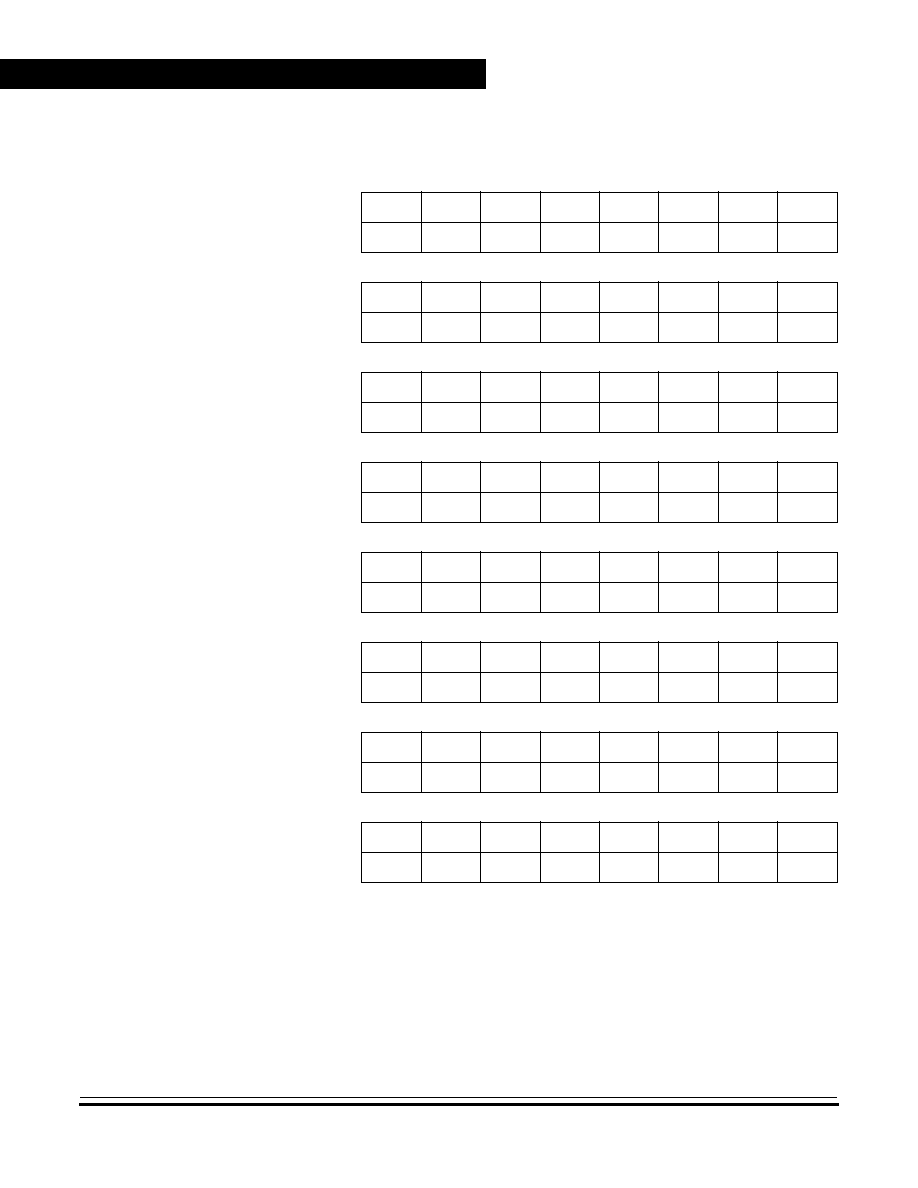
Universal Serial Bus Module (USB)
Advance Information
MC68HC(7)08KH12
--
Rev. 1.0
136
Universal Serial Bus Module (USB)
MOTOROLA
Table 9-4. Embedded Device Data Register Summary
Addr.
Register Name
Bit 7
6
5
4
3
2
1
Bit 0
$0020
USB Embedded Device
Endpoint 0 Data Register 0
(DE0D0)
Read: DE0R07 DE0R06 DE0R05 DE0R04 DE0R03 DE0R02 DE0R01 DE0R00
Write: DE0T07
DE0T06
DE0T05
DE0T04
DE0T03
DE0T02
DE0T01
DE0T00
Reset:
X
X
X
X
X
X
X
X
$0021
USB Embedded Device
Endpoint 0 Data Register 1
(DE0D1)
Read: DE0R17 DE0R16 DE0R15 DE0R14 DE0R13 DE0R12 DE0R11 DE0R10
Write: DE0T17
DE0T16
DE0T15
DE0T14
DE0T13
DE0T12
DE0T11
DE0T10
Reset:
X
X
X
X
X
X
X
X
$0022
USB Embedded Device
Endpoint 0 Data Register 2
(DE0D2)
Read: DE0R27 DE0R26 DE0R25 DE0R24 DE0R23 DE0R22 DE0R21 DE0R20
Write: DE0T27
DE0T26
DE0T25
DE0T24
DE0T23
DE0T22
DE0T21
DE0T20
Reset:
X
X
X
X
X
X
X
X
$0023
USB Embedded Device
Endpoint 0 Data Register 3
(DE0D3)
Read: DE0R37 DE0R36 DE0R35 DE0R34 DE0R33 DE0R32 DE0R31 DE0R30
Write: DE0T37
DE0T36
DE0T35
DE0T34
DE0T33
DE0T32
DE0T31
DE0T30
Reset:
X
X
X
X
X
X
X
X
$0024
USB Embedded Device
Endpoint 0 Data Register 4
(DE0D4)
Read: DE0R47 DE0R46 DE0R45 DE0R44 DE0R43 DE0R42 DE0R41 DE0R40
Write: DE0T47
DE0T46
DE0T45
DE0T44
DE0T43
DE0T42
DE0T41
DE0T40
Reset:
X
X
X
X
X
X
X
X
$0025
USB Embedded Device
Endpoint 0 Data Register 5
(DE0D5)
Read: DE0R57 DE0R56 DE0R55 DE0R54 DE0R53 DE0R52 DE0R51 DE0R50
Write: DE0T57
DE0T56
DE0T55
DE0T54
DE0T53
DE0T52
DE0T51
DE0T50
Reset:
X
X
X
X
X
X
X
X
$0026
USB Embedded Device
Endpoint 0 Data Register 6
(DE0D6)
Read: DE0R67 DE0R66 DE0R65 DE0R64 DE0R63 DE0R62 DE0R61 DE0R60
Write: DE0T67
DE0T66
DE0T65
DE0T64
DE0T63
DE0T62
DE0T61
DE0T60
Reset:
X
X
X
X
X
X
X
X
$0027
USB Embedded Device
Endpoint 0 Data Register 7
(DE0D7)
Read: DE0R77 DE0R76 DE0R75 DE0R74 DE0R73 DE0R72 DE0R71 DE0R70
Write: DE0T77
DE0T76
DE0T75
DE0T74
DE0T73
DE0T72
DE0T71
DE0T70
Reset:
X
X
X
X
X
X
X
X
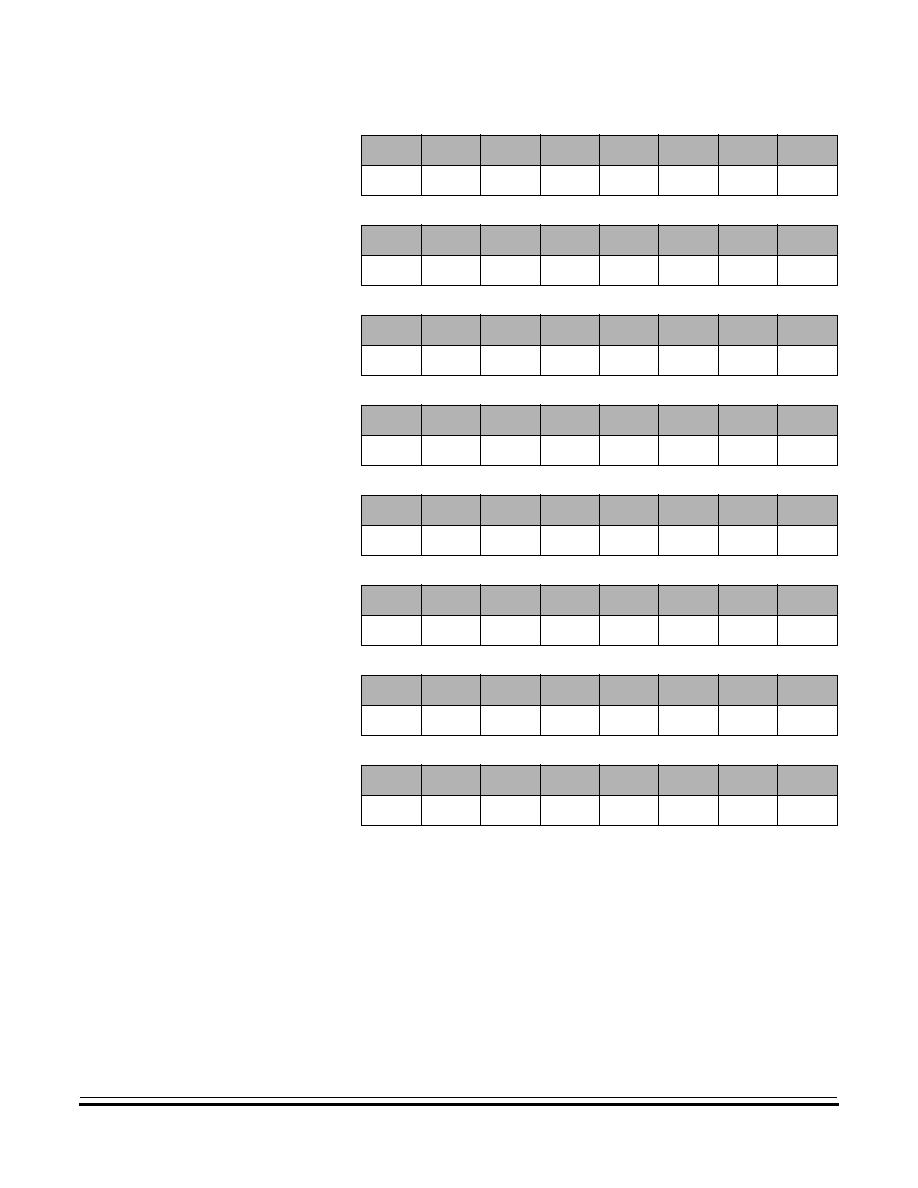
Universal Serial Bus Module (USB)
I/O Register Description of the Embedded Device Function
MC68HC(7)08KH12
--
Rev. 1.0
Advance Information
MOTOROLA
Universal Serial Bus Module (USB)
137
$0028
USB Embedded Device
Endpoint 1/2 Data Register 0
(DE1D0)
Read:
Write: DE1T07
DE1T06
DE1T05
DE1T04
DE1T03
DE1T02
DE1T01
DE1T00
Reset:
X
X
X
X
X
X
X
X
$0029
USB Embedded Device
Endpoint 1/2 Data Register 1
(DE1D1)
Read:
Write: DE1T17
DE1T16
DE1T15
DE1T14
DE1T13
DE1T12
DE1T11
DE1T10
Reset:
X
X
X
X
X
X
X
X
$002A
USB Embedded Device
Endpoint 1/2 Data Register 2
(DE1D2)
Read:
Write: DE1T27
DE1T26
DE1T25
DE1T24
DE1T23
DE1T22
DE1T21
DE1T20
Reset:
X
X
X
X
X
X
X
X
$002B
USB Embedded Device
Endpoint 1/2 Data Register 3
(DE1D3)
Read:
Write: DE1T37
DE1T36
DE1T35
DE1T34
DE1T33
DE1T32
DE1T31
DE1T30
Reset:
X
X
X
X
X
X
X
X
$002C
USB Embedded Device
Endpoint 1/2 Data Register 4
(DE1D4)
Read:
Write: DE1T47
DE1T46
DE1T45
DE1T44
DE1T43
DE1T42
DE1T41
DE1T40
Reset:
X
X
X
X
X
X
X
X
$002D
USB Embedded Device
Endpoint 1/2 Data Register 5
(DE1D5)
Read:
Write: DE1T57
DE1T56
DE1T55
DE1T54
DE1T53
DE1T52
DE1T51
DE1T50
Reset:
X
X
X
X
X
X
X
X
$002E
USB Embedded Device
Endpoint 1/2 Data Register 6
(DE1D6)
Read:
Write: DE1T67
DE1T66
DE1T65
DE1T64
DE1T63
DE1T62
DE1T61
DE1T60
Reset:
X
X
X
X
X
X
X
X
$002F
USB Embedded Device
Endpoint 1/2 Data Register 7
(DE1D7)
Read:
Write: DE1T77
DE1T76
DE1T75
DE1T74
DE1T73
DE1T72
DE1T71
DE1T70
Reset:
X
X
X
X
X
X
X
X
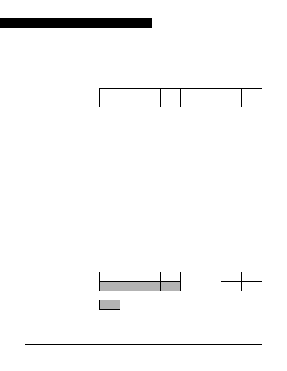
Universal Serial Bus Module (USB)
Advance Information
MC68HC(7)08KH12
--
Rev. 1.0
138
Universal Serial Bus Module (USB)
MOTOROLA
9.5.1 USB Embedded Device Address Register (DADDR)
DEVEN -- Enable USB Embedded Device
These bit enable or disable the embedded device function. It is used
together with PEN1-PEN4 to control the enumeration sequence.
Reset clears these bits.
1 = USB Embedded Device enabled
0 = USB Embedded Device disabled
DADD6-DADD0 -- USB Embedded Device Function Address
These bits specify the address of the embedded device function.
Reset clears these bits.
9.5.2 USB Embedded Device Interrupt Register 0 (DIR0)
Address:
$0048
Bit 7
6
5
4
3
2
1
Bit 0
Read:
DEVEN
DADD6
DADD5
DADD4
DADD3
DADD2
DADD1
DADD0
Write:
Reset:
0
0
0
0
0
0
0
0
Figure 9-12. USB Embedded Device Address Register (DADDR)
Address:
$0049
Bit 7
6
5
4
3
2
1
Bit 0
Read:
TXD0F
RXD0F
0
0
TXD0IE
RXD0IE
0
0
Write:
TXD0FR
RXD0FR
Reset:
0
0
0
0
0
0
0
0
= Unimplemented
Figure 9-13. USB Embedded Device Interrupt Register 0 (DIR0)

Universal Serial Bus Module (USB)
I/O Register Description of the Embedded Device Function
MC68HC(7)08KH12
--
Rev. 1.0
Advance Information
MOTOROLA
Universal Serial Bus Module (USB)
139
TXD0F -- Embedded Device Endpoint 0 Data Transmit Flag
This read only bit is set after the data stored in embedded device
Endpoint 0 transmit buffers has been sent and an ACK handshake
packet from the host is received. Once the next set of data is ready in
the transmit buffers, software must clear this flag by writing a logic 1
to the TXD0FR bit. To enable the next data packet transmission,
TX0E must also be set. If TXD0F bit is not cleared, a NAK handshake
will be returned in the next IN transaction. Reset clears this bit. Writing
to TXD0F has no effect.
1 = Transmit on embedded device Endpoint 0 has occurred
0 = Transmit on embedded device Endpoint 0 has not occurred
RXD0F -- Embedded Device Endpoint 0 Data Receive Flag
This read only bit is set after the USB embedded device module has
received a data packet and responded with an ACK handshake
packet. Software must clear this flag by writing a logic 1 to the
RXD0FR bit after all of the received data has been read. Software
must also set RX0E bit to one to enable the next data packet
reception. If RXD0F bit is not cleared, a NAK handshake will be
returned in the next OUT transaction.
Reset clears this bit. Writing to RXD0F has no effect.
1 = Receive on embedded device Endpoint 0 has occurred
0 = Receive on embedded device Endpoint 0 has not occurred
TXD0IE -- Embedded Device Endpoint 0 Transmit Interrupt Enable
This read/write bit enables the Transmit Embedded Device Endpoint
0 to generate CPU interrupt requests when the TXD0F bit becomes
set. Reset clears the TXD0IE bit.
1 = Transmit Embedded Device Endpoint 0 can generate a CPU
interrupt request
0 = Transmit Embedded Device Endpoint 0 cannot generate a
CPU interrupt request
RXD0IE -- Embedded Device Endpoint 0 Receive Interrupt Enable
This read/write bit enables the Receive Embedded Device Endpoint 0
to generate CPU interrupt requests when the RXD0F bit becomes set.
Reset clears the RXD0IE bit.
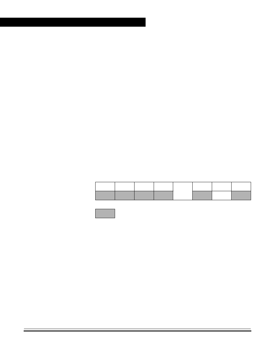
Universal Serial Bus Module (USB)
Advance Information
MC68HC(7)08KH12
--
Rev. 1.0
140
Universal Serial Bus Module (USB)
MOTOROLA
1 = Receive Embedded Device Endpoint 0 can generate a CPU
interrupt request
0 = Receive Embedded Device Endpoint 0 cannot generate a CPU
interrupt request
TXD0FR -- Embedded Device Endpoint 0 Transmit Flag Reset
Writing a logic 1 to this write only bit will clear the TXD0F bit if it is set.
Writing a logic 0 to TXD0FR has no effect. Reset clears this bit.
RXD0FR -- Embedded Device Endpoint 0 Receive Flag Reset
Writing a logic 1 to this write only bit will clear the RXD0F bit if it is set.
Writing a logic 0 to RXD0FR has no effect. Reset clears this bit.
9.5.3 USB Embedded Device Interrupt Register 1 (DIR1)
TXD1F -- Embedded Device Endpoint 1/2 Data Transmit Flag
This read only bit is shared by Endpoint 1 and Endpoint 2 of the
embedded device. It is set after the data stored in the shared Endpoint
1/2 transmit buffer of the embedded device has been sent and an
ACK handshake packet from the host is received. Once the next set
of data is ready in the transmit buffers, software must clear this flag
by writing a logic 1 to the TXD1FR bit. To enable the next data packet
transmission, TX1E must also be set. If TXD1F bit is not cleared, a
NAK handshake will be returned in the next IN transaction. Reset
clears this bit. Writing to TXD1F has no effect.
Address:
$004A
Bit 7
6
5
4
3
2
1
Bit 0
Read:
TXD1F
0
0
0
TXD1IE
0
0
0
Write:
TXD1FR
Reset:
0
0
0
0
0
0
0
0
= Unimplemented
Figure 9-14. USB Embedded Device Interrupt Register 1 (DIR1)

Universal Serial Bus Module (USB)
I/O Register Description of the Embedded Device Function
MC68HC(7)08KH12
--
Rev. 1.0
Advance Information
MOTOROLA
Universal Serial Bus Module (USB)
141
1 = Transmit on Endpoint 1 or Endpoint 2 of the embedded device
has occurred
0 = Transmit on Endpoint 1 or Endpoint 2 of the embedded device
has not occurred
TXD1IE -- Embedded Device Endpoint 1/2 Transmit Interrupt Enable
This read/write bit enables the USB to generate CPU interrupt
requests when the shared Transmit Endpoint 1/2 interrupt flag bit of
the embedded device (TXD1F) becomes set. Reset clears the
TXD1IE bit.
1 = Transmit embedded device Endpoints 1 and 2 can generate a
CPU interrupt request
0 = Transmit embedded device Endpoints 1 and 2 cannot generate
a CPU interrupt request
TXD1FR -- Embedded Device Endpoint 1/2 Transmit Flag Reset
Writing a logic 1 to this write only bit will clear the TXD1F bit if it is set.
Writing a logic 0 to TXD1FR has no effect. Reset clears this bit.
9.5.4 USB Embedded Device Control Register 0 (DCR0)
T0SEQ -- Embedded Device Endpoint 0 Transmit Sequence Bit
This read/write bit determines which type of data packet (DATA0 or
DATA1) will be sent during the next IN transaction directed at
Endpoint 0. Toggling of this bit must be controlled by software. Reset
clears this bit.
Address:
$004B
Bit 7
6
5
4
3
2
1
Bit 0
Read:
T0SEQ
DSTALL0
TX0E
RX0E
TP0SIZ3
TP0SIZ2
TP0SIZ1
TP0SIZ0
Write:
Reset:
0
0
0
0
0
0
0
0
Figure 9-15. USB Embedded Device Control Register 0 (DCR0)

Universal Serial Bus Module (USB)
Advance Information
MC68HC(7)08KH12
--
Rev. 1.0
142
Universal Serial Bus Module (USB)
MOTOROLA
1 = DATA1 Token active for next embedded device Endpoint 0
transmit
0 = DATA0 Token active for next embedded device Endpoint 0
transmit
DSTALL0 -- Embedded Device Endpoint 0 Force Stall Bit
This read/write bit causes embedded device Endpoint 0 to return a
STALL handshake when polled by either an IN or OUT token by the
host. The USB hardware clears this bit when a SETUP token is
received. Reset clears this bit.
1 = Send STALL handshake
0 = Default
TX0E -- Embedded Device Endpoint 0 Transmit Enable
This read/write bit enables a transmit to occur when the USB Host
controller sends an IN token to the embedded device Endpoint 0.
Software should set this bit when data is ready to be transmitted. It
must be cleared by software when no more embedded device
Endpoint 0 data needs to be transmitted.
If this bit is 0 or the TXD0F is set, the USB will respond with a NAK
handshake to any embedded device Endpoint 0 IN tokens. Reset
clears this bit.
1 = Data is ready to be sent
0 = Data is not ready. Respond with NAK
RX0E -- Embedded Device Endpoint 0 Receive Enable
This read/write bit enables a receive to occur when the USB Host
controller sends an OUT token to the embedded device Endpoint 0.
Software should set this bit when data is ready to be received. It must
be cleared by software when data cannot be received.
If this bit is 0 or the RXD0F is set, the USB will respond with a NAK
handshake to any embedded device Endpoint 0 OUT tokens. Reset
clears this bit.
1 = Data is ready to be received
0 = Not ready for data. Respond with NAK

Universal Serial Bus Module (USB)
I/O Register Description of the Embedded Device Function
MC68HC(7)08KH12
--
Rev. 1.0
Advance Information
MOTOROLA
Universal Serial Bus Module (USB)
143
TP0SIZ3-TP0SIZ0 -- Embedded Device Endpoint 0 Transmit Data
Packet Size
These read/write bits store the number of transmit data bytes for the
next IN token request for embedded device Endpoint 0. These bits
are cleared by reset.
9.5.5 USB Embedded Device Control Register 1 (DCR1)
T1SEQ -- Embedded Device Endpoint 1/2 Transmit Sequence Bit
This read/write bit determines which type of data packet (DATA0 or
DATA1) will be sent during the next IN transaction directed to
embedded device Endpoint 1 or 2. Toggling of this bit must be
controlled by software. Reset clears this bit.
1 = DATA1 Token active for next embedded device Endpoint 1/2
transmit
0 = DATA0 Token active for next embedded device Endpoint 1/2
transmit
ENDADD -- Endpoint Address Select
This read/write bit specifies whether the data inside the registers
DE1D0-DE1D7 are used for embedded device Endpoint 1 or 2. If all
the conditions for a successful Endpoint 2 USB response to a host's
IN token are satisfied (TXD1F=0, TX1E=1, DSTALL2=0, and
ENABLE2=1) except that the ENDADD bit is configured for
Endpoint 1, the USB responds with a NAK handshake packet. Reset
clears this bit.
Address:
$004C
Bit 7
6
5
4
3
2
1
Bit 0
Read:
T1SEQ
ENDADD
TX1E
0
TP1SIZ3
TP1SIZ2
TP1SIZ1
TP1SIZ0
Write:
Reset:
0
0
0
0
0
0
0
0
= Unimplemented
Figure 9-16. USB Embedded Device Control Register 1 (DCR1)
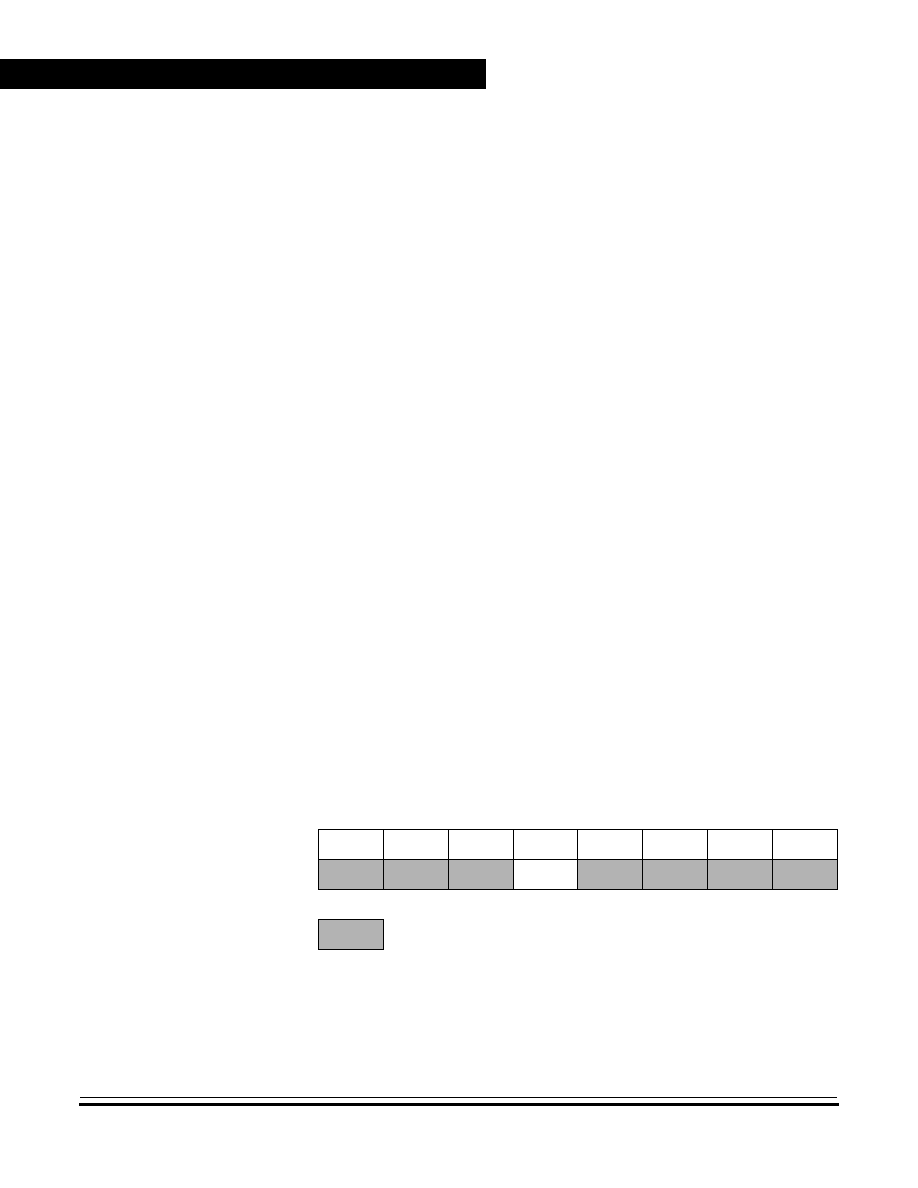
Universal Serial Bus Module (USB)
Advance Information
MC68HC(7)08KH12
--
Rev. 1.0
144
Universal Serial Bus Module (USB)
MOTOROLA
1 = The data buffers are used for embedded device Endpoint 2
0 = The data buffers are used for embedded device Endpoint 1
TX1E -- Embedded Device Endpoint 1/2 Transmit Enable
This read/write bit enables a transmit to occur when the USB Host
controller sends an IN token to Endpoint 1 or Endpoint 2 of the
embedded device. The appropriate endpoint enable bit, ENABLE1 or
ENABLE2 bit in the DCR2 register, should also be set. Software
should set the TX1E bit when data is ready to be transmitted. It must
be cleared by software when no more data needs to be transmitted.
If this bit is 0 or the TXD1F is set, the USB will respond with a NAK
handshake to any Endpoint 1 or Endpoint 2 directed IN tokens. Reset
clears this bit.
1 = Data is ready to be sent.
0 = Data is not ready. Respond with NAK.
TP1SIZ3-TP1SIZ0 -- Embedded Device Endpoint 1/2 Transmit Data
Packet Size
These read/write bits store the number of transmit data bytes for the
next IN token request for embedded device Endpoint 1 or Endpoint 2.
These bits are cleared by reset.
9.5.6 USB Embedded Device Status Register (DSR)
Address:
$004D
Bit 7
6
5
4
3
2
1
Bit 0
Read:
DRSEQ
DSETUP
DTX1ST
0
RP0SIZ3
RPS0IZ2
RP0SIZ1
RP0SIZ0
Write:
DTX1STR
Reset:
X
X
0
0
X
X
X
X
= Unimplemented
X = Indeterminate
Figure 9-17. USB Embedded Device Status Register (DSR)

Universal Serial Bus Module (USB)
I/O Register Description of the Embedded Device Function
MC68HC(7)08KH12
--
Rev. 1.0
Advance Information
MOTOROLA
Universal Serial Bus Module (USB)
145
DRSEQ -- Embedded Device Endpoint 0 Receive Sequence Bit
This read only bit indicates the type of data packet last received for
embedded device Endpoint 0 (DATA0 or DATA1).
1 = DATA1 Token received in last embedded device Endpoint 0
receive
0 = DATA0 Token received in last embedded device Endpoint 0
receive
DSETUP -- Embedded Device SETUP Token Detect Bit
This read only bit indicates that a valid SETUP token has been
received.
1 = Last token received for Endpoint 0 was a SETUP token
0 = Last token received for Endpoint 0 was not a SETUP token
DTX1ST -- Embedded Device Transmit First Flag
This read only bit is set if the embedded device Endpoint 0 Data
Transmit Flag (TXD0F) is set when the USB control logic is setting the
embedded device Endpoint 0 Data Receive Flag (RXD0F). In other
words, if an unserviced Endpoint 0 Transmit Flag is still set at the end
of an endpoint 0 reception, then this bit will be set. This bit lets the
firmware know that the Endpoint 0 transmission happened before the
Endpoint 0 reception. Reset clears this bit.
1 = IN transaction occurred before SETUP/OUT
0 = IN transaction occurred after SETUP/OUT
DTX1STR -- Clear Transmit First Flag
Writing a logic 1 to this write only bit will clear the DTX1ST bit if it is
set. Writing a logic 0 to the DTX1STR has no effect. Reset clears this
bit.
RP0SIZ3-RP0SIZ0 -- Embedded Device Endpoint 0 Receive Data
Packet Size
These read only bits store the number of data bytes received for the
last OUT or SETUP transaction for embedded device Endpoint 0.
These bits are not affected by reset.
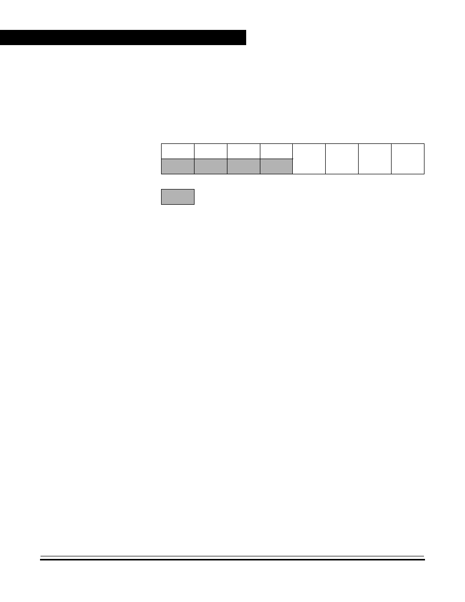
Universal Serial Bus Module (USB)
Advance Information
MC68HC(7)08KH12
--
Rev. 1.0
146
Universal Serial Bus Module (USB)
MOTOROLA
9.5.7 USB Embedded Device Control Register 2 (DCR2)
ENABLE2 -- Embedded Device Endpoint 2 Enable
This read/write bit enables embedded device Endpoint 2 and allows
the USB to respond to IN packets addressed to this endpoint. Reset
clears this bit.
1 = Embedded device Endpoint 2 is enabled and can respond to
an IN token
0 = Embedded device Endpoint 2 is disabled
ENABLE1 -- Embedded Device Endpoint 1 Enable
This read/write bit enables embedded device Endpoint 1 and allows
the USB to respond to IN packets addressed to this endpoint. Reset
clears this bit.
1 = Embedded device Endpoint 1 is enabled and can respond to
an IN token
0 = Embedded device Endpoint 1 is disabled
DSTALL2 -- Embedded Device Endpoint 2 Force Stall Bit
This read/write bit causes embedded device Endpoint 2 to return a
STALL handshake when polled by either an IN or OUT token by the
USB Host Controller. Reset clears this bit.
1 = Send STALL handshake
0 = Default
Address:
$0047
Bit 7
6
5
4
3
2
1
Bit 0
Read:
0
0
0
0
ENABLE2 ENABLE1 DSTALL2 DSTALL1
Write:
Reset:
0
0
0
0
0
0
0
0
= Unimplemented
Figure 9-18. USB Embedded Device Control Register 2 (DCR2)

Universal Serial Bus Module (USB)
I/O Register Description of the Embedded Device Function
MC68HC(7)08KH12
--
Rev. 1.0
Advance Information
MOTOROLA
Universal Serial Bus Module (USB)
147
DSTALL1 -- Embedded Device Endpoint 1 Force Stall Bit
This read/write bit causes embedded device Endpoint 1 to return a
STALL handshake when polled by either an IN or OUT token by the
USB Host Controller. Reset clears this bit.
1 = Send STALL handshake
0 = Default
9.5.8 USB Embedded Device Endpoint 0 Data Registers (DE0D0-DE0D7)
DE0Rx7-DE0Rx0 -- Embedded Device Endpoint 0 Receive Data Buffer
These read only bits are serially loaded with OUT token or SETUP
token data directed at embedded device Endpoint 0. The data is
received over the USB's D0+ and D0≠ pins.
DE0Tx7-DE0Tx0 -- Embedded Device Endpoint 0 Transmit Data Buffer
These write only buffers are loaded by software with data to be sent
on the USB bus on the next IN token directed at embedded device
Endpoint 0.
Address: $0020
Bit 7
6
5
4
3
2
1
Bit 0
Read: DE0R07
DE0R06
DE0R05
DE0R04
DE0R03
DE0R02
DE0R01
DE0R00
Write:
DE0T07
DE0T06
DE0T05
DE0T04
DE0T03
DE0T02
DE0T01
DE0T00
Reset:
X
X
X
X
X
X
X
X
Address: $0027
Read: DE0R77
DE0R76
DE0R75
DE0R74
DE0R73
DE0R72
DE0R71
DE0R70
Write:
DE0T77
DE0T76
DE0T75
DE0T74
DE0T73
DE0T72
DE0T71
DE0T70
Reset:
X
X
X
X
X
X
X
X
X = Indeterminate
Figure 9-19. USB Embedded Device Endpoint 0 Data Register
(UE0D0-UE0D7)
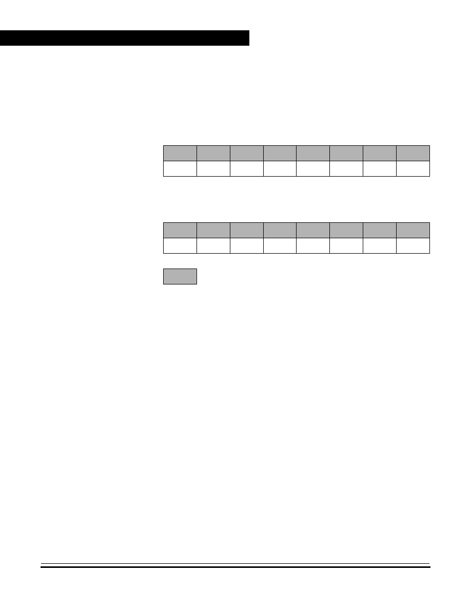
Universal Serial Bus Module (USB)
Advance Information
MC68HC(7)08KH12
--
Rev. 1.0
148
Universal Serial Bus Module (USB)
MOTOROLA
9.5.9 USB Embedded Device Endpoint 1/2 Data Registers (DE1D0-DE1D7)
DE1TD7-DE1TD0 -- Embedded Device Endpoint 1/ Endpoint 2
Transmit Data Buffer
These write only buffers are loaded by software with data to be sent
on the USB bus on the next IN token directed at Endpoint 1 or
Endpoint 2 of the embedded device. These buffers are shared by
embedded device Endpoints 1 and 2 and depend on proper
configuration of the ENDADD bit.
Address: $0028
Bit 7
6
5
4
3
2
1
Bit 0
Read:
Write:
DE1T07
DE1T06
DE1T05
DE1T04
DE1T03
DE1T02
DE1T01
DE1T00
Reset:
X
X
X
X
X
X
X
X
Address: $002F
Read:
Write:
DE1T77
DE1T76
DE1T75
DE1T74
DE1T73
DE1T72
DE1T71
DE1T70
Reset:
X
X
X
X
X
X
X
X
= Unimplemented
X = Indeterminate
Figure 9-20. USB Embedded Device Endpoint 0 Data Register
(UE0D0-UE0D7)

MC68HC(7)08KH12
--
Rev. 1.0
Advance Information
MOTOROLA
Monitor ROM (MON)
149
Advance Information -- MC68HC(7)08KH12
Section 10. Monitor ROM (MON)
10.1 Contents
10.2
Introduction . . . . . . . . . . . . . . . . . . . . . . . . . . . . . . . . . . . . . . . 149
10.3
Features . . . . . . . . . . . . . . . . . . . . . . . . . . . . . . . . . . . . . . . . . 150
10.4
Functional Description . . . . . . . . . . . . . . . . . . . . . . . . . . . . . . 150
10.4.1
Entering Monitor Mode . . . . . . . . . . . . . . . . . . . . . . . . . . . 152
10.4.2
Data Format . . . . . . . . . . . . . . . . . . . . . . . . . . . . . . . . . . . 154
10.4.3
Echoing . . . . . . . . . . . . . . . . . . . . . . . . . . . . . . . . . . . . . . . 154
10.4.4
Break Signal . . . . . . . . . . . . . . . . . . . . . . . . . . . . . . . . . . . 155
10.4.5
Commands . . . . . . . . . . . . . . . . . . . . . . . . . . . . . . . . . . . . 155
10.4.6
Baud Rate . . . . . . . . . . . . . . . . . . . . . . . . . . . . . . . . . . . . . 159
10.2 Introduction
This section describes the monitor ROM. The monitor ROM allows
complete testing of the MCU through a single-wire interface with a host
computer.

Monitor ROM (MON)
Advance Information
MC68HC(7)08KH12
--
Rev. 1.0
150
Monitor ROM (MON)
MOTOROLA
10.3 Features
Features of the monitor ROM include the following:
∑
Normal User-Mode Pin Functionality
∑
One Pin Dedicated to Serial Communication between Monitor
ROM and Host Computer
∑
Standard Mark/Space Non-Return-to-Zero (NRZ) Communication
with Host Computer
∑
4800 Baud to 28.8 kBaud Communication with Host Computer
∑
Execution of Code in RAM or ROM
∑
OTPROM Programming
10.4 Functional Description
The monitor ROM receives and executes commands from a host
computer.
Figure 10-1
shows a sample circuit used to enter monitor
mode and communicate with a host computer via a standard RS-232
interface.
Simple monitor commands can access any memory address. In monitor
mode, the MCU can execute host-computer code in RAM while all MCU
pins retain normal operating mode functions. All communication
between the host computer and the MCU is through the PTA0 pin. A
level-shifting and multiplexing interface is required between PTA0 and
the host computer. PTA0 is used in a wired-OR configuration and
requires a pull-up resistor.
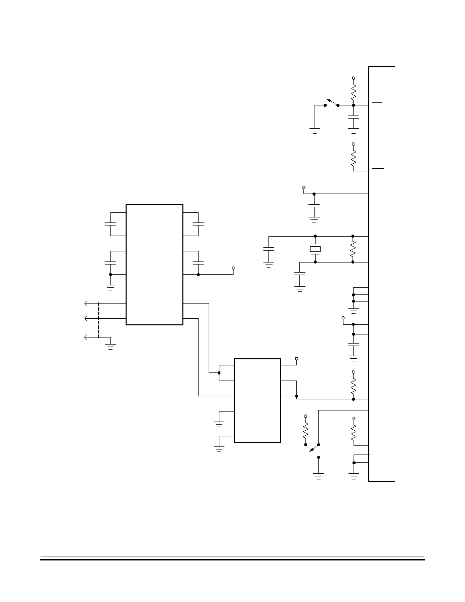
Monitor ROM (MON)
Functional Description
MC68HC(7)08KH12
--
Rev. 1.0
Advance Information
MOTOROLA
Monitor ROM (MON)
151
Figure 10-1. Monitor Mode Circuit
+
+
+
+
10M
X1
V
DD
V
DD
+ V
HI
MC145407
MC74HC125
68HC708
RST
IRQ1/V
PP
OSC1
OSC2
V
SS2
V
SSA
V
DD
1
PA0
V
DD
10k
0.1
µ
F
10
6
5
2
4
3
1
DB-25
2
3
7
20
18
17
19
16
15
V
DD
V
DD
V
DD
20pF
20pF
10
µ
F
10
µ
F
10
µ
F
10
µ
F
1
2
4
7
14
3
0.1
µ
F
4.9152MHz
10 k
PC3
V
DD
10k
B
A
NOTES: Position A -- Bus clock = CGMXCLK
˜
4
Position B -- Bus clock = CGMXCLK
˜
2
(See NOTE.)
5
6
V
SS1
PC0
PC1
V
DD
10k
V
DDA
0.1
µ
F
V
DD
PA7
V
DD
2
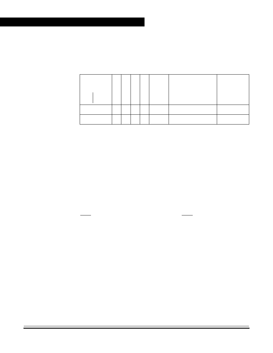
Monitor ROM (MON)
Advance Information
MC68HC(7)08KH12
--
Rev. 1.0
152
Monitor ROM (MON)
MOTOROLA
10.4.1 Entering Monitor Mode
Table 10-1
shows the pin conditions for entering monitor mode.
If PTC3 is low upon monitor mode entry, CGMOUT is equal to the crystal
frequency. The bus frequency in this case is a divide-by-two of the input
clock. If PTC3 is high upon monitor mode entry, the bus frequency will
be a divide-by-four of the input clock.
NOTE:
Holding the PTC3 pin low when entering monitor mode causes a bypass
of a divide-by-two stage at the oscillator. The CGMOUT frequency is
equal to the CGMXCLK frequency, and the OSC1 input directly
generates internal bus clocks. In this case, the OSC1 signal must have
a 50% duty cycle at maximum bus frequency.
Enter monitor mode with the pin configuration shown above by pulling
RST low and then high. The rising edge of RST latches monitor mode.
Once monitor mode is latched, the values on the specified pins can
change.
Once out of reset, the MCU monitor mode firmware then sends a break
signal (10 consecutive logic zeros) to the host computer, indicating that
it is ready to receive a command. The break signal also provides a timing
reference to allow the host to determine the necessary baud rate.
Monitor mode uses different vectors for reset, SWI, and break interrupt.
The alternate vectors are in the $FE page instead of the $FF page and
allow code execution from the internal monitor firmware instead of user
code.
Table 10-1. Mode Selection
IRQ1
/V
PP
Pin
PC0 Pin
PC1 Pin
PA0 Pin
PC3 Pin
Mode
CGMOUT
Bus
Frequency
V
DD
+ V
HI
1
0
1
1
Monitor
CGMXCLK ˜ 2
CGMOUT ˜ 2
V
DD
+ V
HI
1
0
1
0
Monitor
CGMXCLK
CGMOUT ˜ 2
Monitor ROM (MON)
Functional Description
MC68HC(7)08KH12
--
Rev. 1.0
Advance Information
MOTOROLA
Monitor ROM (MON)
153
When the host computer has completed downloading code into the MCU
RAM, This code can be executed by driving PTA0 low while asserting
RST low and then high. The internal monitor ROM firmware will interpret
the low on PTA0 as an indication to jump to RAM, and execution control
will then continue from RAM. Execution of an SWI from the downloaded
code will return program control to the internal monitor ROM firmware.
Alternatively, the host can send a RUN command, which executes an
RTI, and this can be used to send control to the address on the stack
pointer.
The COP module is disabled in monitor mode as long as V
DD
+ V
HI
is
applied to either the IRQ1/V
PP
pin or the RST pin. (
See
Section 7.
System Integration Module (SIM)
for more information on modes of
operation.)
Table 10-2
is a summary of the differences between user mode and
monitor mode.
Table 10-2. Mode Differences
Modes
Functions
COP
Reset
Vector
High
Reset
Vector
Low
Break
Vector
High
Break
Vector
Low
SWI
Vector
High
SWI
Vector
Low
User
Enabled
$FFFE
$FFFF
$FFFC
$FFFD
$FFFC
$FFFD
Monitor
Disabled
(1)
1. If the high voltage (V
DD
+ V
HI
) is removed from the IRQ1/V
PP
pin or the RST pin, the SIM
asserts its COP enable output. The COP is a mask option enabled or disabled by the
COPD bit in the configuration register.
$FEFE
$FEFF
$FEFC
$FEFD
$FEFC
$FEFD

Monitor ROM (MON)
Advance Information
MC68HC(7)08KH12
--
Rev. 1.0
154
Monitor ROM (MON)
MOTOROLA
10.4.2 Data Format
Communication with the monitor ROM is in standard non-return-to-zero
(NRZ) mark/space data format. (See
Figure 10-2
and
Figure 10-3
.)
Figure 10-2. Monitor Data Format
Figure 10-3. Sample Monitor Waveforms
The data transmit and receive rate can be anywhere from 4800 baud to
28.8 kbaud. Transmit and receive baud rates must be identical.
10.4.3 Echoing
As shown in
Figure 10-4
, the monitor ROM immediately echoes each
received byte back to the PTA0 pin for error checking.
Figure 10-4. Read Transaction
Any result of a command appears after the echo of the last byte of the
command.
BIT 5
START
BIT
BIT 0
BIT 1
NEXT
STOP
BIT
START
BIT
BIT 2
BIT 3
BIT 4
BIT 6
BIT 7
BIT 5
START
BIT
BIT 0
BIT 1
NEXT
STOP
BIT
START
BIT
BIT 2
BIT 3
BIT 4
BIT 6
BIT 7
START
BIT
BIT 0
BIT 1
NEXT
STOP
BIT
START
BIT
BIT 2
$A5
BREAK
BIT 3
BIT 4
BIT 5
BIT 6
BIT 7
ADDR. HIGH
READ
READ
ADDR. HIGH
ADDR. LOW
ADDR. LOW
DATA
ECHO
SENT TO
MONITOR
RESULT
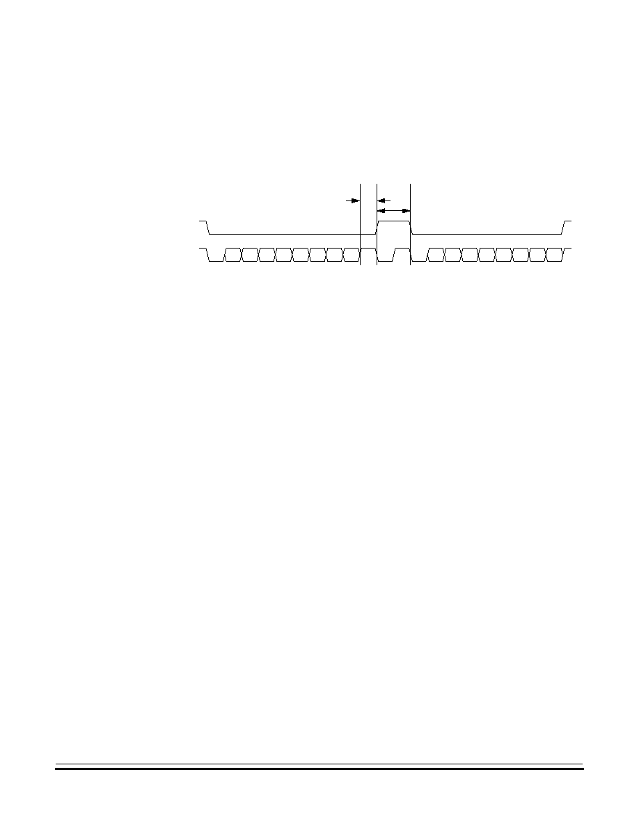
Monitor ROM (MON)
Functional Description
MC68HC(7)08KH12
--
Rev. 1.0
Advance Information
MOTOROLA
Monitor ROM (MON)
155
10.4.4 Break Signal
A start bit followed by nine low bits is a break signal.
(See Figure 10-5.)
When the monitor receives a break signal, it drives the PTA0 pin high for
the duration of two bits before echoing the break signal.
Figure 10-5. Break Transaction
10.4.5 Commands
The monitor ROM uses the following commands:
∑
READ (read memory)
∑
WRITE (write memory)
∑
IREAD (indexed read)
∑
IWRITE (indexed write)
∑
READSP (read stack pointer)
∑
RUN (run user program)
0
1
2
3
4
5
6
7
0
1
2
3
4
5
6
7
MISSING STOP BIT
TWO-STOP-BIT DELAY BEFORE ZERO ECHO
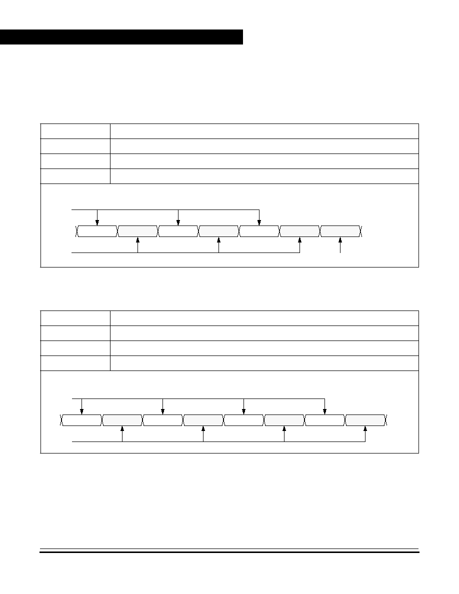
Monitor ROM (MON)
Advance Information
MC68HC(7)08KH12
--
Rev. 1.0
156
Monitor ROM (MON)
MOTOROLA
Table 10-3. READ (Read Memory) Command
Description
Read byte from memory
Operand
Specifies 2-byte address in high byte:low byte order
Data Returned
Returns contents of specified address
Opcode
$4A
Command Sequence
ADDR. HIGH
READ
READ
ADDR. HIGH
ADDR. LOW
ADDR. LOW
DATA
ECHO
SENT TO
MONITOR
RESULT
Table 10-4. WRITE (Write Memory) Command
Description
Write byte to memory
Operand
Specifies 2-byte address in high byte:low byte order; low byte followed by data byte
Data Returned
None
Opcode
$49
Command Sequence
ADDR. HIGH
WRITE
WRITE
ADDR. HIGH
ADDR. LOW
ADDR. LOW
DATA
ECHO
SENT TO
MONITOR
DATA
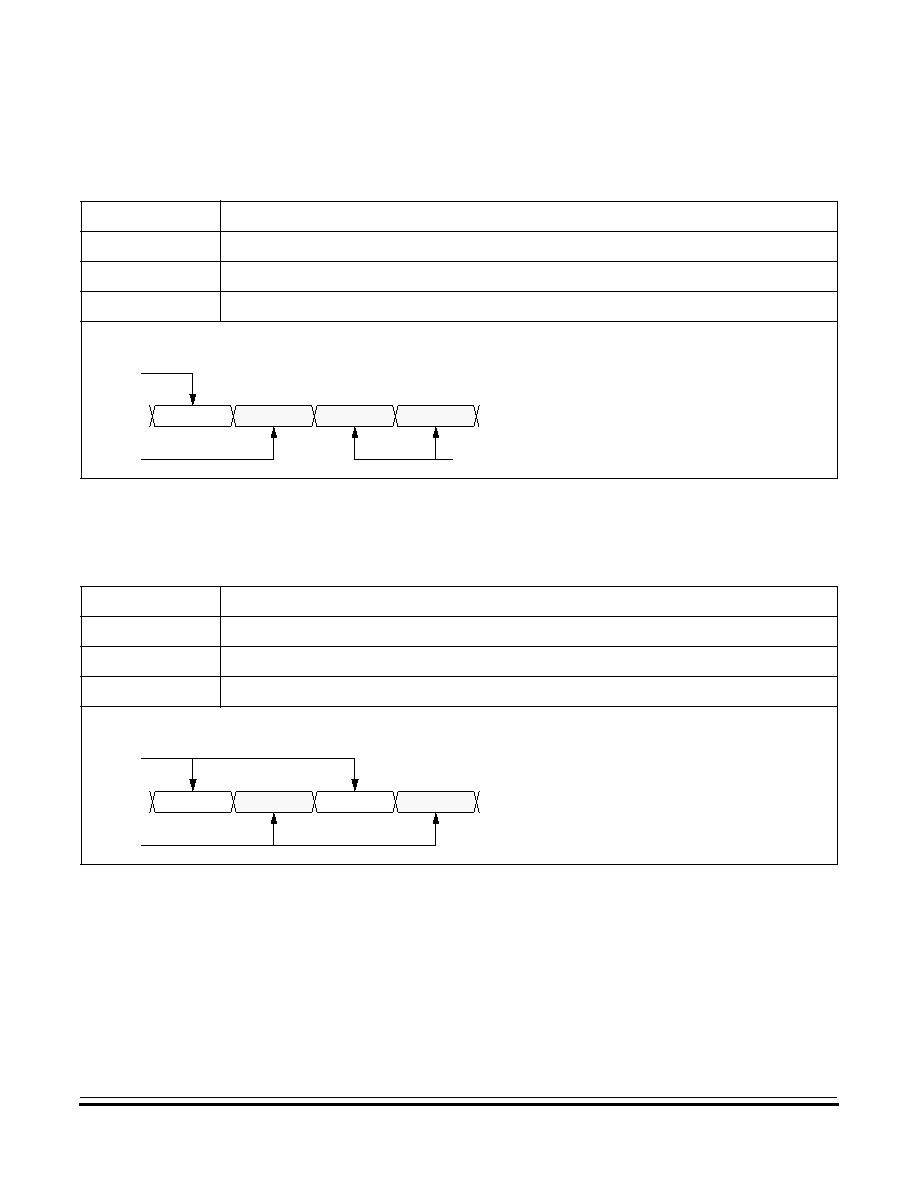
Monitor ROM (MON)
Functional Description
MC68HC(7)08KH12
--
Rev. 1.0
Advance Information
MOTOROLA
Monitor ROM (MON)
157
Table 10-5. IREAD (Indexed Read) Command
Description
Read next 2 bytes in memory from last address accessed
Operand
Specifies 2-byte address in high byte:low byte order
Data Returned
Returns contents of next two addresses
Opcode
$1A
Command Sequence
DATA
IREAD
IREAD
DATA
ECHO
SENT TO
MONITOR
RESULT
Table 10-6. IWRITE (Indexed Write) Command
Description
Write to last address accessed + 1
Operand
Specifies single data byte
Data Returned
None
Opcode
$19
Command Sequence
DATA
IWRITE
IWRITE
DATA
ECHO
SENT TO
MONITOR
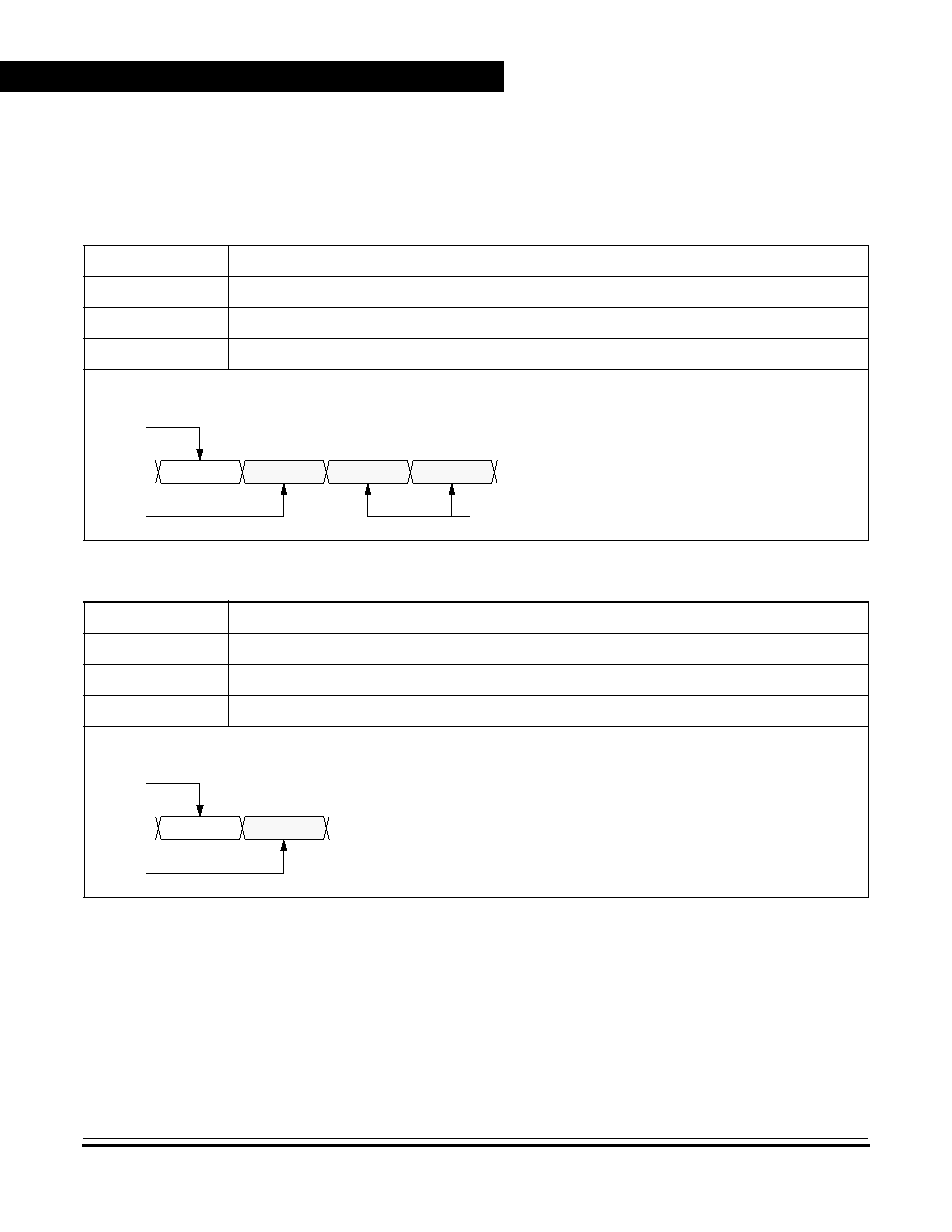
Monitor ROM (MON)
Advance Information
MC68HC(7)08KH12
--
Rev. 1.0
158
Monitor ROM (MON)
MOTOROLA
NOTE:
A sequence of IREAD or IWRITE commands can sequentially access a
block of memory over the full 64-Kbyte memory map.
Table 10-7. READSP (Read Stack Pointer) Command
Description
Reads stack pointer
Operand
None
Data Returned
Returns stack pointer in high byte:low byte order
Opcode
$0C
Command Sequence
Table 10-8. RUN (Run User Program) Command
Description
Executes RTI instruction
Operand
None
Data Returned
None
Opcode
$28
Command Sequence
SP HIGH
READSP
READSP
SP LOW
ECHO
SENT TO
MONITOR
RESULT
RUN
RUN
ECHO
SENT TO
MONITOR

Monitor ROM (MON)
Functional Description
MC68HC(7)08KH12
--
Rev. 1.0
Advance Information
MOTOROLA
Monitor ROM (MON)
159
10.4.6 Baud Rate
The communication baud rate is controlled by crystal frequency and the
state of the PTC3 pin upon entry into monitor mode. When PTC3 is high,
the divide by ratio is 1024. If the PTC3 pin is at logic zero upon entry into
monitor mode, the divide by ratio is 512.
Table 10-9. Monitor Baud Rate Selection
Crystal
Frequency
(MHz)
PTC3
pin
Baud Rate
4.9152MHz
0
9600 bps
4.9152MHz
1
4800 bps

Monitor ROM (MON)
Advance Information
MC68HC(7)08KH12
--
Rev. 1.0
160
Monitor ROM (MON)
MOTOROLA

MC68HC(7)08KH12
--
Rev. 1.0
Advance Information
MOTOROLA
Timer Interface Module (TIM)
161
Advance Information -- MC68HC(7)08KH12
Section 11. Timer Interface Module (TIM)
11.1 Contents
11.2
Introduction . . . . . . . . . . . . . . . . . . . . . . . . . . . . . . . . . . . . . . . 162
11.3
Features . . . . . . . . . . . . . . . . . . . . . . . . . . . . . . . . . . . . . . . . . 162
11.4
Functional Description . . . . . . . . . . . . . . . . . . . . . . . . . . . . . . 163
11.4.1
TIM Counter Prescaler . . . . . . . . . . . . . . . . . . . . . . . . . . . 165
11.4.2
Input Capture. . . . . . . . . . . . . . . . . . . . . . . . . . . . . . . . . . . 165
11.4.3
Output Compare . . . . . . . . . . . . . . . . . . . . . . . . . . . . . . . . 165
11.4.3.1
Unbuffered Output Compare . . . . . . . . . . . . . . . . . . . . . 166
11.4.3.2
Buffered Output Compare . . . . . . . . . . . . . . . . . . . . . . . 166
11.4.4
Pulse Width Modulation (PWM) . . . . . . . . . . . . . . . . . . . . 167
11.4.4.1
Unbuffered PWM Signal Generation . . . . . . . . . . . . . . . 168
11.4.4.2
Buffered PWM Signal Generation . . . . . . . . . . . . . . . . . 169
11.4.4.3
PWM Initialization . . . . . . . . . . . . . . . . . . . . . . . . . . . . . 170
11.5
Interrupts. . . . . . . . . . . . . . . . . . . . . . . . . . . . . . . . . . . . . . . . . 171
11.6
Wait Mode. . . . . . . . . . . . . . . . . . . . . . . . . . . . . . . . . . . . . . . . 171
11.7
TIM During Break Interrupts . . . . . . . . . . . . . . . . . . . . . . . . . . 172
11.8
I/O Signals . . . . . . . . . . . . . . . . . . . . . . . . . . . . . . . . . . . . . . . 172
11.8.1
TIM Clock Pin (PTE0/TCLK) . . . . . . . . . . . . . . . . . . . . . . . 172
11.8.2
TIM Channel I/O Pins (PTE1/TCH0:PTE2/TCH1). . . . . . . 173
11.9
I/O Registers. . . . . . . . . . . . . . . . . . . . . . . . . . . . . . . . . . . . . . 173
11.9.1
TIM Status and Control Register (TSC) . . . . . . . . . . . . . . 173
11.9.2
TIM Counter Registers (TCNTH:TCNTL) . . . . . . . . . . . . . 175
11.9.3
TIM Counter Modulo Registers (TMODH:TMODL) . . . . . . 176
11.9.4
TIM Channel Status and Control Registers (TSC0:TSC1) 177
11.9.5
TIM Channel Registers (TCH0H/L≠TCH1H/L) . . . . . . . . . 181

Timer Interface Module (TIM)
Advance Information
MC68HC(7)08KH12
--
Rev. 1.0
162
Timer Interface Module (TIM)
MOTOROLA
11.2 Introduction
This section describes the timer interface module (TIM2, Version B). The
TIM is a two-channel timer that provides a timing reference with input
capture, output compare, and pulse-width-modulation functions.
Figure
11-1
is a block diagram of the TIM.
11.3 Features
Features of the TIM include the following:
∑
Two Input Capture/Output Compare Channels
≠
Rising-Edge, Falling-Edge, or Any-Edge Input Capture Trigger
≠
Set, Clear, or Toggle Output Compare Action
∑
Buffered and Unbuffered Pulse Width Modulation (PWM) Signal
Generation
∑
Programmable TIM Clock Input
≠
Seven-Frequency Internal Bus Clock Prescaler Selection
≠
External TIM Clock Input (4-MHz Maximum Frequency)
∑
Free-Running or Modulo Up-Count Operation
∑
Toggle Any Channel Pin on Overflow
∑
TIM Counter Stop and Reset Bits
∑
Modular Architecture Expandable to Eight Channels
Timer Interface Module (TIM)
Functional Description
MC68HC(7)08KH12
--
Rev. 1.0
Advance Information
MOTOROLA
Timer Interface Module (TIM)
163
11.4 Functional Description
Figure 11-1
shows the structure of the TIM. The central component of
the TIM is the 16-bit TIM counter that can operate as a free-running
counter or a modulo up-counter. The TIM counter provides the timing
reference for the input capture and output compare functions. The TIM
counter modulo registers, TMODH:TMODL, control the modulo value of
the TIM counter. Software can read the TIM counter value at any time
without affecting the counting sequence.
The two TIM channels are programmable independently as input
capture or output compare channels.
Figure 11-1. TIM Block Diagram
PRESCALER
PRESCALER SELECT
16-BIT COMPARATOR
PS2
PS1
PS0
16-BIT COMPARATOR
16-BIT LATCH
TCH0H:TCH0L
MS0A
ELS0B
ELS0A
TOF
TOIE
16-BIT COMPARATOR
16-BIT LATCH
TCH1H:TCH1L
CHANNEL 0
CHANNEL 1
TMODH:TMODL
TRST
TSTOP
TOV0
CH0IE
CH0F
ELS1B
ELS1A
TOV1
CH1IE
CH1MAX
CH1F
CH0MAX
MS0B
16-BIT COUNTER
INTERNAL BUS
MS1A
TCLK
PTE0/TCLK
INTERNAL
BUS CLOCK
PTE2/TCH1
PTE1/TCH0
INTERRUPT
LOGIC
PTE2
LOGIC
INTERRUPT
LOGIC
INTERRUPT
LOGIC
PTE1
LOGIC
Timer Interface Module (TIM)
Advance Information
MC68HC(7)08KH12
--
Rev. 1.0
164
Timer Interface Module (TIM)
MOTOROLA
Table 11-1. TIM I/O Register Summary
Addr.
Register Name
Bit 7
6
5
4
3
2
1
Bit 0
$0010
TIM Status/Control Register
(TSC)
Read:
TOF
TOIE
TSTOP
0
0
PS2
PS1
PS0
Write:
0
TRST
Reset:
0
0
1
0
0
0
0
0
$0012
TIM Counter Register High
(TCNTH)
Read:
Bit15
Bit14
Bit13
Bit12
Bit11
Bit10
Bit9
Bit8
Write:
Reset:
0
0
0
0
0
0
0
0
$0013
TIM Counter Register Low
(TCNTL)
Read:
Bit7
Bit6
Bit5
Bit4
Bit3
Bit2
Bit1
Bit0
Write:
Reset:
0
0
0
0
0
0
0
0
$0014
TIM Counter Modulo
Register High
(TMODH)
Read:
Bit15
Bit14
Bit13
Bit12
Bit11
Bit10
Bit9
Bit8
Write:
Reset:
1
1
1
1
1
1
1
1
$0015
TIM Counter Modulo
Register Low
(TMODL)
Read:
Bit7
Bit6
Bit5
Bit4
Bit3
Bit2
Bit1
Bit0
Write:
Reset:
1
1
1
1
1
1
1
1
$0016
TIM Channel 0
Status/Control Register
(TSC0)
Read:
CH0F
CH0IE
MS0B
MS0A
ELS0B
ELS0A
TOV0
CH0MAX
Write:
0
Reset:
0
0
0
0
0
0
0
0
$0017
TIM Channel 0
Register High
(TCH0H)
Read:
Bit15
Bit14
Bit13
Bit12
Bit11
Bit10
Bit9
Bit8
Write:
Reset:
X
X
X
X
X
X
X
X
$0018
TIM Channel 0
Register Low
(TCH0L)
Read:
Bit7
Bit6
Bit5
Bit4
Bit3
Bit2
Bit1
Bit0
Write:
Reset:
X
X
X
X
X
X
X
X
$0019
TIM Channel 1
Status/Control Register
(TSC1)
Read:
CH1F
CH1IE
0
MS1A
ELS1B
ELS1A
TOV1
CH1MAX
Write:
0
Reset:
0
0
0
0
0
0
0
0

Timer Interface Module (TIM)
Functional Description
MC68HC(7)08KH12
--
Rev. 1.0
Advance Information
MOTOROLA
Timer Interface Module (TIM)
165
11.4.1 TIM Counter Prescaler
The TIM clock source can be one of the seven prescaler outputs or the
TIM clock pin, PTE0/TCLK. The prescaler generates seven clock rates
from the internal bus clock. The prescaler select bits, PS[2:0], in the TIM
status and control register (TSC) select the TIM clock source.
11.4.2 Input Capture
With the input capture function, the TIM can capture the time at which an
external event occurs. When an active edge occurs on the pin of an input
capture channel, the TIM latches the contents of the TIM counter into the
TIM channel registers, TCHxH:TCHxL. The polarity of the active edge is
programmable. Input captures can generate TIM CPU interrupt
requests.
11.4.3 Output Compare
With the output compare function, the TIM can generate a periodic pulse
with a programmable polarity, duration, and frequency. When the
counter reaches the value in the registers of an output compare channel,
the TIM can set, clear, or toggle the channel pin. Output compares can
generate TIM CPU interrupt requests.
$001A
TIM Channel 1
Register High
(TCH1H)
Read:
Bit15
Bit14
Bit13
Bit12
Bit11
Bit10
Bit9
Bit8
Write:
Reset:
X
X
X
X
X
X
X
X
$001B
TIM Channel 1
Register Low
(TCH1L)
Read:
Bit7
Bit6
Bit5
Bit4
Bit3
Bit2
Bit1
Bit0
Write:
Reset:
X
X
X
X
X
X
X
X
= Unimplemented
X = Indeterminate

Timer Interface Module (TIM)
Advance Information
MC68HC(7)08KH12
--
Rev. 1.0
166
Timer Interface Module (TIM)
MOTOROLA
11.4.3.1 Unbuffered Output Compare
Any output compare channel can generate unbuffered output compare
pulses as described in
11.4.3 Output Compare
. The pulses are
unbuffered because changing the output compare value requires writing
the new value over the old value currently in the TIM channel registers.
An unsynchronized write to the TIM channel registers to change an
output compare value could cause incorrect operation for up to two
counter overflow periods. For example, writing a new value before the
counter reaches the old value but after the counter reaches the new
value prevents any compare during that counter overflow period. Also,
using a TIM overflow interrupt routine to write a new, smaller output
compare value may cause the compare to be missed. The TIM may pass
the new value before it is written.
Use the following methods to synchronize unbuffered changes in the
output compare value on channel x:
∑
When changing to a smaller value, enable channel x output
compare interrupts and write the new value in the output compare
interrupt routine. The output compare interrupt occurs at the end
of the current output compare pulse. The interrupt routine has until
the end of the counter overflow period to write the new value.
∑
When changing to a larger output compare value, enable
channel x TIM overflow interrupts and write the new value in the
TIM overflow interrupt routine. The TIM overflow interrupt occurs
at the end of the current counter overflow period. Writing a larger
value in an output compare interrupt routine (at the end of the
current pulse) could cause two output compares to occur in the
same counter overflow period.
11.4.3.2 Buffered Output Compare
Channels 0 and 1 can be linked to form a buffered output compare
channel whose output appears on the PTE1/TCH0 pin. The TIM channel
registers of the linked pair alternately control the output.
Setting the MS0B bit in TIM channel 0 status and control register (TSC0)
links channel 0 and channel 1. The output compare value in the TIM

Timer Interface Module (TIM)
Functional Description
MC68HC(7)08KH12
--
Rev. 1.0
Advance Information
MOTOROLA
Timer Interface Module (TIM)
167
channel 0 registers initially controls the output on the PTE1/TCH0 pin.
Writing to the TIM channel 1 registers enables the TIM channel 1
registers to synchronously control the output after the TIM overflows. At
each subsequent overflow, the TIM channel registers (0 or 1) that control
the output are the ones written to last. TSC0 controls and monitors the
buffered output compare function, and TIM channel 1 status and control
register (TSC1) is unused. While the MS0B bit is set, the channel 1 pin,
PTE2/TCH1, is available as a general-purpose I/O pin.
NOTE:
In buffered output compare operation, do not write new output compare
values to the currently active channel registers. Writing to the active
channel registers is the same as generating unbuffered output
compares.
11.4.4 Pulse Width Modulation (PWM)
By using the toggle-on-overflow feature with an output compare channel,
the TIM can generate a PWM signal. The value in the TIM counter
modulo registers determines the period of the PWM signal. The channel
pin toggles when the counter reaches the value in the TIM counter
modulo registers. The time between overflows is the period of the PWM
signal.
As
Figure 11-2
shows, the output compare value in the TIM channel
registers determines the pulse width of the PWM signal. The time
between overflow and output compare is the pulse width. Program the
TIM to clear the channel pin on output compare if the state of the PWM
pulse is logic one. Program the TIM to set the pin if the state of the PWM
pulse is logic zero.

Timer Interface Module (TIM)
Advance Information
MC68HC(7)08KH12
--
Rev. 1.0
168
Timer Interface Module (TIM)
MOTOROLA
Figure 11-2. PWM Period and Pulse Width
The value in the TIM counter modulo registers and the selected
prescaler output determines the frequency of the PWM output. The
frequency of an 8-bit PWM signal is variable in 256 increments. Writing
$00FF (255) to the TIM counter modulo registers produces a PWM
period of 256 times the internal bus clock period if the prescaler select
value is 000
(see 11.9.1 TIM Status and Control Register (TSC)
).
The value in the TIM channel registers determines the pulse width of the
PWM output. The pulse width of an 8-bit PWM signal is variable in 256
increments. Writing $0080 (128) to the TIM channel registers produces
a duty cycle of 128/256 or 50%.
11.4.4.1 Unbuffered PWM Signal Generation
Any output compare channel can generate unbuffered PWM pulses as
described in
11.4.4 Pulse Width Modulation (PWM)
. The pulses are
unbuffered because changing the pulse width requires writing the new
pulse width value over the old value currently in the TIM channel
registers.
An unsynchronized write to the TIM channel registers to change a pulse
width value could cause incorrect operation for up to two PWM periods.
For example, writing a new value before the counter reaches the old
value but after the counter reaches the new value prevents any compare
during that PWM period. Also, using a TIM overflow interrupt routine to
PTEx/TCHxA
PERIOD
PULSE
WIDTH
OVERFLOW
OVERFLOW
OVERFLOW
OUTPUT
COMPARE
OUTPUT
COMPARE
OUTPUT
COMPARE

Timer Interface Module (TIM)
Functional Description
MC68HC(7)08KH12
--
Rev. 1.0
Advance Information
MOTOROLA
Timer Interface Module (TIM)
169
write a new, smaller pulse width value may cause the compare to be
missed. The TIM may pass the new value before it is written.
Use the following methods to synchronize unbuffered changes in the
PWM pulse width on channel x:
∑
When changing to a shorter pulse width, enable channel x output
compare interrupts and write the new value in the output compare
interrupt routine. The output compare interrupt occurs at the end
of the current pulse. The interrupt routine has until the end of the
PWM period to write the new value.
∑
When changing to a longer pulse width, enable channel x TIM
overflow interrupts and write the new value in the TIM overflow
interrupt routine. The TIM overflow interrupt occurs at the end of
the current PWM period. Writing a larger value in an output
compare interrupt routine (at the end of the current pulse) could
cause two output compares to occur in the same PWM period.
NOTE:
In PWM signal generation, do not program the PWM channel to toggle
on output compare. Toggling on output compare prevents reliable 0%
duty cycle generation and removes the ability of the channel to
self-correct in the event of software error or noise. Toggling on output
compare also can cause incorrect PWM signal generation when
changing the PWM pulse width to a new, much larger value.
11.4.4.2 Buffered PWM Signal Generation
Channels 0 and 1 can be linked to form a buffered PWM channel whose
output appears on the PTE1/TCH0 pin. The TIM channel registers of the
linked pair alternately control the pulse width of the output.
Setting the MS0B bit in TIM channel 0 status and control register (TSC0)
links channel 0 and channel 1. The TIM channel 0 registers initially
control the pulse width on the PTE1/TCH0 pin. Writing to the TIM
channel 1 registers enables the TIM channel 1 registers to
synchronously control the pulse width at the beginning of the next PWM
period. At each subsequent overflow, the TIM channel registers (0 or 1)
that control the pulse width are the ones written to last. TSC0 controls
and monitors the buffered PWM function, and TIM channel 1 status and

Timer Interface Module (TIM)
Advance Information
MC68HC(7)08KH12
--
Rev. 1.0
170
Timer Interface Module (TIM)
MOTOROLA
control register (TSC1) is unused. While the MS0B bit is set, the channel
1 pin, PTE2/TCH1, is available as a general-purpose I/O pin.
NOTE:
In buffered PWM signal generation, do not write new pulse width values
to the currently active channel registers. Writing to the active channel
registers is the same as generating unbuffered PWM signals.
11.4.4.3 PWM Initialization
To ensure correct operation when generating unbuffered or buffered
PWM signals, use the following initialization procedure:
1. In the TIM status and control register (TSC):
a.
Stop the TIM counter by setting the TIM stop bit, TSTOP.
b.
Reset the TIM counter by setting the TIM reset bit, TRST.
2. In the TIM counter modulo registers (TMODH:TMODL), write the
value for the required PWM period.
3. In the TIM channel x registers (TCHxH:TCHxL), write the value for
the required pulse width.
4. In TIM channel x status and control register (TSCx):
a.
Write 0:1 (for unbuffered output compare or PWM signals) or
1:0 (for buffered output compare or PWM signals) to the mode
select bits, MSxB:MSxA.
(See Table 11-3.)
b.
Write 1 to the toggle-on-overflow bit, TOVx.
c.
Write 1:0 (to clear output on compare) or 1:1 (to set output on
compare) to the edge/level select bits, ELSxB:ELSxA. The
output action on compare must force the output to the
complement of the pulse width level. (See
Table 11-3
.)
NOTE:
In PWM signal generation, do not program the PWM channel to toggle
on output compare. Toggling on output compare prevents reliable 0%
duty cycle generation and removes the ability of the channel to
self-correct in the event of software error or noise. Toggling on output
compare can also cause incorrect PWM signal generation when
changing the PWM pulse width to a new, much larger value.
5. In the TIM status control register (TSC), clear the TIM stop bit,
TSTOP.

Timer Interface Module (TIM)
Interrupts
MC68HC(7)08KH12
--
Rev. 1.0
Advance Information
MOTOROLA
Timer Interface Module (TIM)
171
Setting MS0B links channels 0 and 1 and configures them for buffered
PWM operation. The TIM channel 0 registers (TCH0H:TCH0L) initially
control the buffered PWM output. TIM status control register 0 (TSCR0)
controls and monitors the PWM signal from the linked channels. MS0B
takes priority over MS0A.
Clearing the toggle-on-overflow bit, TOVx, inhibits output toggles on TIM
overflows. Subsequent output compares try to force the output to a state
it is already in and have no effect. The result is a 0% duty cycle output.
Setting the channel x maximum duty cycle bit (CHxMAX) and clearing
the TOVx bit generates a 100% duty cycle output. See
11.9.4 TIM
Channel Status and Control Registers (TSC0:TSC1)
.
11.5 Interrupts
The following TIM sources can generate interrupt requests:
∑
TIM overflow flag (TOF) -- The TOF bit is set when the TIM
counter value rolls over to $0000 after matching the value in the
TIM counter modulo registers. The TIM overflow interrupt enable
bit, TOIE, enables TIM overflow CPU interrupt requests. TOF and
TOIE are in the TIM status and control register.
∑
TIM channel flags (CH1F:CH0F) -- The CHxF bit is set when an
input capture or output compare occurs on channel x. Channel x
TIM CPU interrupt requests are controlled by the channel x
interrupt enable bit, CHxIE. Channel x TIM CPU interrupt requests
are enabled when CHxIE=1. CHxF and CHxIE are in the TIM
channel x status and control register.
11.6 Wait Mode
The WAIT instruction puts the MCU in low-power-consumption standby
mode.
The TIM remains active after the execution of a WAIT instruction. In wait
mode the TIM registers are not accessible by the CPU. Any enabled
CPU interrupt request from the TIM can bring the MCU out of wait mode.

Timer Interface Module (TIM)
Advance Information
MC68HC(7)08KH12
--
Rev. 1.0
172
Timer Interface Module (TIM)
MOTOROLA
If TIM functions are not required during wait mode, reduce power
consumption by stopping the TIM before executing the WAIT instruction.
11.7 TIM During Break Interrupts
A break interrupt stops the TIM counter.
The system integration module (SIM) controls whether status bits in
other modules can be cleared during the break state. The BCFE bit in
the break flag control register (BFCR) enables software to clear status
bits during the break state.
(See 7.8.3 Break Flag Control Register
(BFCR)
.)
To allow software to clear status bits during a break interrupt, write a
logic one to the BCFE bit. If a status bit is cleared during the break state,
it remains cleared when the MCU exits the break state.
To protect status bits during the break state, write a logic zero to the
BCFE bit. With BCFE at logic zero (its default state), software can read
and write I/O registers during the break state without affecting status
bits. Some status bits have a two-step read/write clearing procedure. If
software does the first step on such a bit before the break, the bit cannot
change during the break state as long as BCFE is at logic zero. After the
break, doing the second step clears the status bit.
11.8 I/O Signals
Port E shares three of its pins with the TIM. PTE0/TCLK is and external
clock input to the TIM prescaler. The two TIM channel I/O pins are
PTE1/TCH0 and PTE2/TCH1.
11.8.1 TIM Clock Pin (PTE0/TCLK)
PTE0/TCLK is an external clock input that can be the clock source for
the TIM counter instead of the prescaled internal bus clock. Select the
PTE0/TCLK input by writing logic ones to the three prescaler select bits,
PS[2:0].
(See 11.9.1 TIM Status and Control Register (TSC)
.) The

Timer Interface Module (TIM)
I/O Registers
MC68HC(7)08KH12
--
Rev. 1.0
Advance Information
MOTOROLA
Timer Interface Module (TIM)
173
minimum TCLK pulse width, TCLK
LMIN
or TCLK
HMIN
, is:
The maximum TCLK frequency is:
PTE0/TCLK is available as a general-purpose I/O pin when not used as
the TIM clock input. When the PTE0/TCLK pin is the TIM clock input, it
is an input regardless of the state of the DDRE0 bit in data direction
register E.
11.8.2 TIM Channel I/O Pins (PTE1/TCH0:PTE2/TCH1)
Each channel I/O pin is programmable independently as an input
capture pin or an output compare pin. PTE1/TCH0 can be configured as
buffered output compare or buffered PWM pins.
11.9 I/O Registers
The following I/O registers control and monitor operation of the TIM:
∑
TIM status and control register (TSC)
∑
TIM control registers (TCNTH:TCNTL)
∑
TIM counter modulo registers (TMODH:TMODL)
∑
TIM channel status and control registers (TSC0 and TSC1)
∑
TIM channel registers (TCH0H:TCH0L and TCH1H:TCH1L)
11.9.1 TIM Status and Control Register (TSC)
The TIM status and control register does the following:
∑
Enables TIM overflow interrupts
∑
Flags TIM overflows
∑
Stops the TIM counter
1
bus frequency
-------------------------------------
t
SU
+
bus frequency
2
-------------------------------------
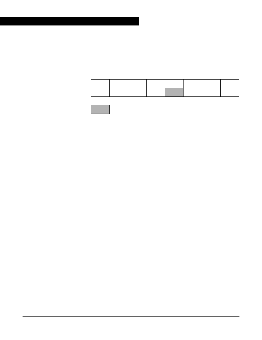
Timer Interface Module (TIM)
Advance Information
MC68HC(7)08KH12
--
Rev. 1.0
174
Timer Interface Module (TIM)
MOTOROLA
∑
Resets the TIM counter
∑
Prescales the TIM counter clock
TOF -- TIM Overflow Flag Bit
This read/write flag is set when the TIM counter resets to $0000 after
reaching the modulo value programmed in the TIM counter modulo
registers. Clear TOF by reading the TIM status and control register
when TOF is set and then writing a logic zero to TOF. If another TIM
overflow occurs before the clearing sequence is complete, then
writing logic zero to TOF has no effect. Therefore, a TOF interrupt
request cannot be lost due to inadvertent clearing of TOF. Reset
clears the TOF bit. Writing a logic one to TOF has no effect.
1 = TIM counter has reached modulo value
0 = TIM counter has not reached modulo value
TOIE -- TIM Overflow Interrupt Enable Bit
This read/write bit enables TIM overflow interrupts when the TOF bit
becomes set. Reset clears the TOIE bit.
1 = TIM overflow interrupts enabled
0 = TIM overflow interrupts disabled
TSTOP -- TIM Stop Bit
This read/write bit stops the TIM counter. Counting resumes when
TSTOP is cleared. Reset sets the TSTOP bit, stopping the TIM
counter until software clears the TSTOP bit.
1 = TIM counter stopped
0 = TIM counter active
Address:
$0010
Bit 7
6
5
4
3
2
1
Bit 0
Read:
TOF
TOIE
TSTOP
0
0
PS2
PS1
PS0
Write:
0
TRST
Reset:
0
0
1
0
0
0
0
0
= Unimplemented
Figure 11-3. TIM Status and Control Register (TSC)
Timer Interface Module (TIM)
I/O Registers
MC68HC(7)08KH12
--
Rev. 1.0
Advance Information
MOTOROLA
Timer Interface Module (TIM)
175
NOTE:
Do not set the TSTOP bit before entering wait mode if the TIM is required
to exit wait mode.
TRST -- TIM Reset Bit
Setting this write-only bit resets the TIM counter and the TIM
prescaler. Setting TRST has no effect on any other registers.
Counting resumes from $0000. TRST is cleared automatically after
the TIM counter is reset and always reads as logic zero. Reset clears
the TRST bit.
1 = Prescaler and TIM counter cleared
0 = No effect
NOTE:
Setting the TSTOP and TRST bits simultaneously stops the TIM counter
at a value of $0000.
PS[2:0] -- Prescaler Select Bits
These read/write bits select either the PTE0/TCLK pin or one of the
seven prescaler outputs as the input to the TIM counter as
Table 11-2
shows. Reset clears the PS[2:0] bits.
11.9.2 TIM Counter Registers (TCNTH:TCNTL)
The two read-only TIM counter registers contain the high and low bytes
of the value in the TIM counter. Reading the high byte (TCNTH) latches
the contents of the low byte (TCNTL) into a buffer. Subsequent reads of
Table 11-2. Prescaler Selection
PS2
PS1
PS0
TIM Clock Source
0
0
0
Internal Bus Clock ˜ 1
0
0
1
Internal Bus Clock ˜ 2
0
1
0
Internal Bus Clock ˜ 4
0
1
1
Internal Bus Clock ˜ 8
1
0
0
Internal Bus Clock ˜ 16
1
0
1
Internal Bus Clock ˜ 32
1
1
0
Internal Bus Clock ˜ 64
1
1
1
PTE0/TCLK
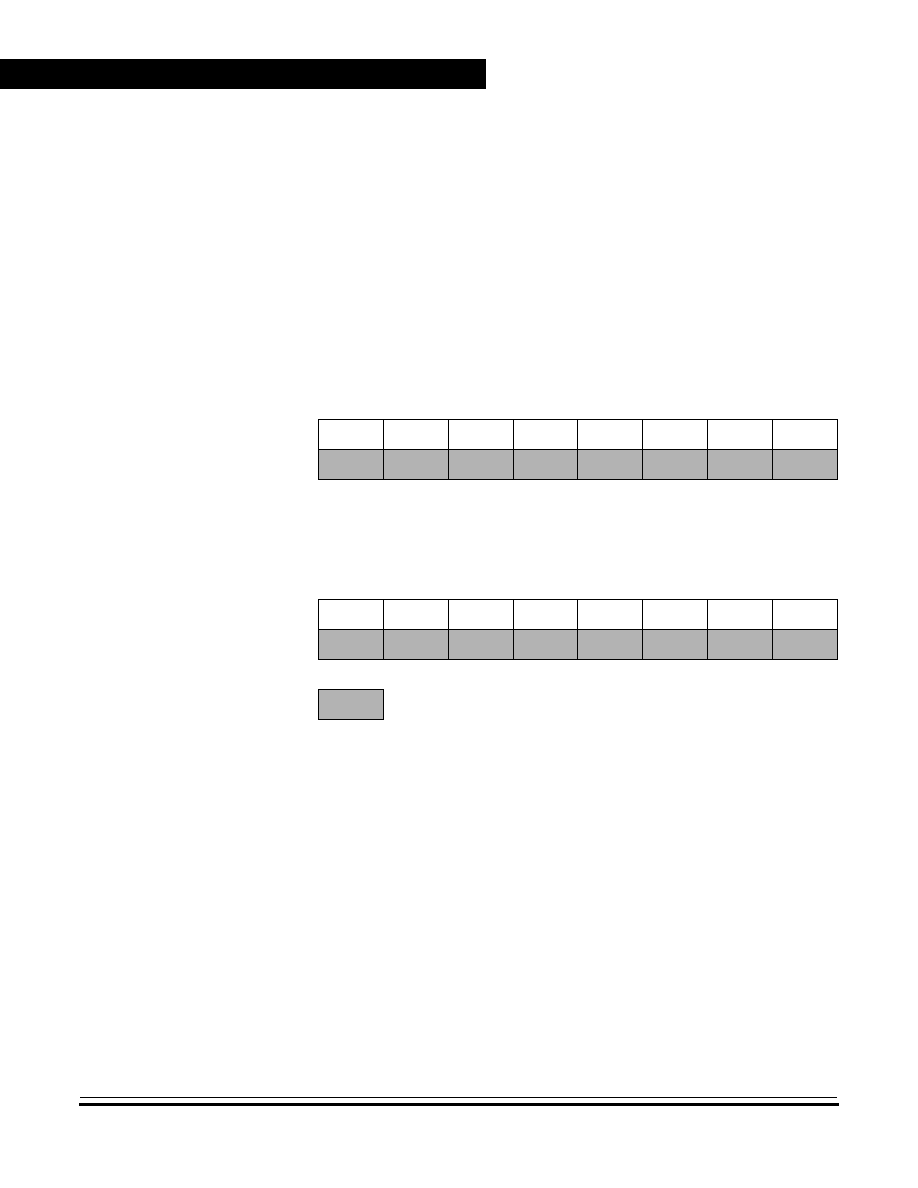
Timer Interface Module (TIM)
Advance Information
MC68HC(7)08KH12
--
Rev. 1.0
176
Timer Interface Module (TIM)
MOTOROLA
TCNTH do not affect the latched TCNTL value until TCNTL is read.
Reset clears the TIM counter registers. Setting the TIM reset bit (TRST)
also clears the TIM counter registers.
NOTE:
If you read TCNTH during a break interrupt, be sure to unlatch TCNTL
by reading TCNTL before exiting the break interrupt. Otherwise, TCNTL
retains the value latched during the break.
11.9.3 TIM Counter Modulo Registers (TMODH:TMODL)
The read/write TIM modulo registers contain the modulo value for the
TIM counter. When the TIM counter reaches the modulo value, the
overflow flag (TOF) becomes set, and the TIM counter resumes counting
from $0000 at the next clock. Writing to the high byte (TMODH) inhibits
the TOF bit and overflow interrupts until the low byte (TMODL) is written.
Reset sets the TIM counter modulo registers.
Address:
$0012
TCNTH
Bit 7
6
5
4
3
2
1
Bit 0
Read:
Bit15
Bit14
Bit13
Bit12
Bit11
Bit10
Bit9
Bit8
Write:
Reset:
0
0
0
0
0
0
0
0
Address:
$0013
TCNTL
Bit 7
6
5
4
3
2
1
Bit 0
Read:
Bit7
Bit6
Bit5
Bit4
Bit3
Bit2
Bit1
Bit0
Write:
Reset:
0
0
0
0
0
0
0
0
= Unimplemented
Figure 11-4. TIM Counter Registers (TCNTH:TCNTL)

Timer Interface Module (TIM)
I/O Registers
MC68HC(7)08KH12
--
Rev. 1.0
Advance Information
MOTOROLA
Timer Interface Module (TIM)
177
NOTE:
Reset the TIM counter before writing to the TIM counter modulo registers.
11.9.4 TIM Channel Status and Control Registers (TSC0:TSC1)
Each of the TIM channel status and control registers does the following:
∑
Flags input captures and output compares
∑
Enables input capture and output compare interrupts
∑
Selects input capture, output compare, or PWM operation
∑
Selects high, low, or toggling output on output compare
∑
Selects rising edge, falling edge, or any edge as the active input
capture trigger
∑
Selects output toggling on TIM overflow
∑
Selects 100% PWM duty cycle
∑
Selects buffered or unbuffered output compare/PWM operation
Address:
$0014
TMODH
Bit 7
6
5
4
3
2
1
Bit 0
Read:
Bit15
Bit14
Bit13
Bit12
Bit11
Bit10
Bit9
Bit8
Write:
Reset:
1
1
1
1
1
1
1
1
Address:
$0015
TMODL
Bit 7
6
5
4
3
2
1
Bit 0
Read:
Bit7
Bit6
Bit5
Bit4
Bit3
Bit2
Bit1
Bit0
Write:
Reset:
1
1
1
1
1
1
1
1
Figure 11-5. TIM Counter Modulo Registers (TMODH:TMODL)
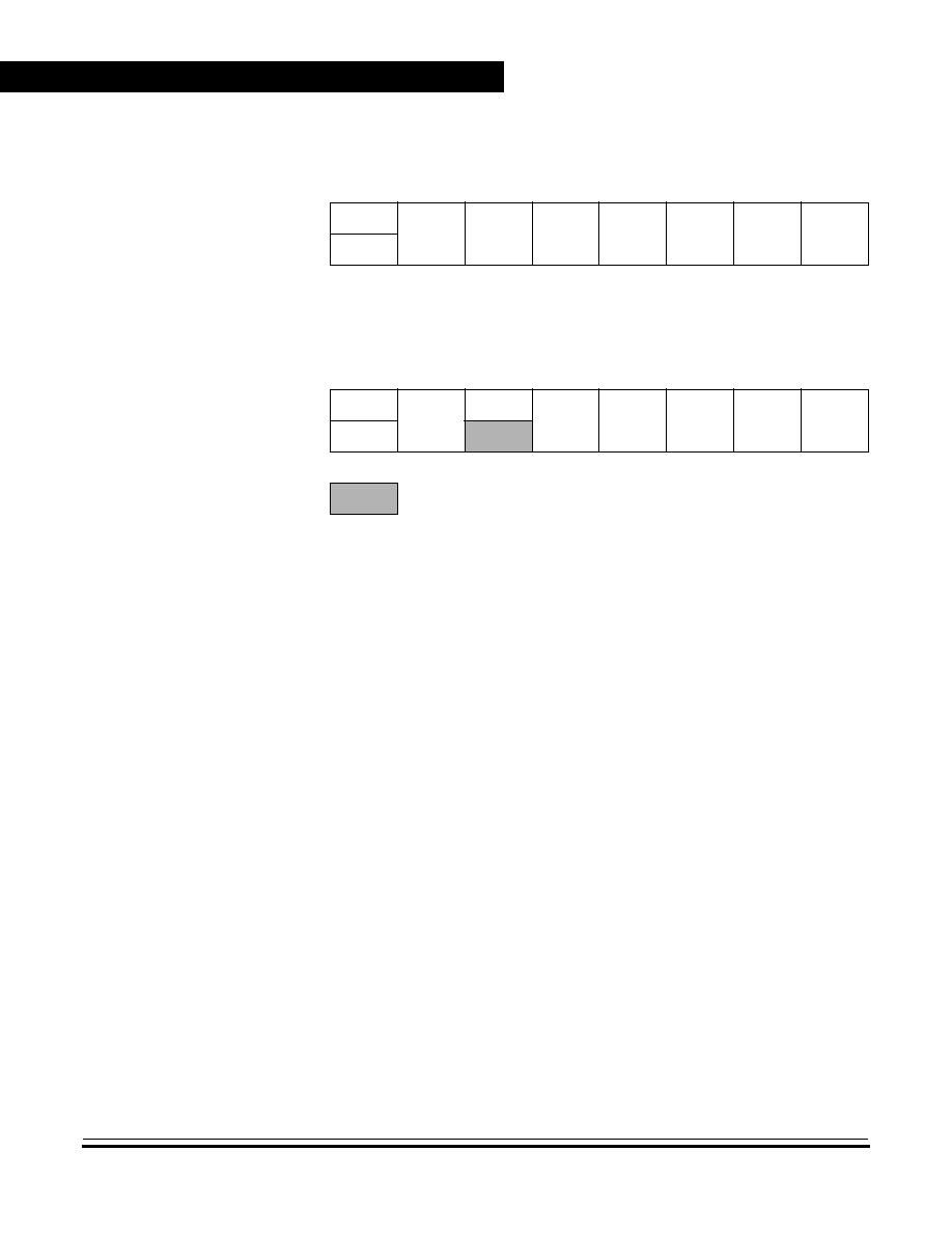
Timer Interface Module (TIM)
Advance Information
MC68HC(7)08KH12
--
Rev. 1.0
178
Timer Interface Module (TIM)
MOTOROLA
CHxF -- Channel x Flag Bit
When channel x is an input capture channel, this read/write bit is set
when an active edge occurs on the channel x pin. When channel x is
an output compare channel, CHxF is set when the value in the TIM
counter registers matches the value in the TIM channel x registers.
When TIM CPU interrupt requests are enabled (CHxIE=1), clear
CHxF by reading the TIM channel x status and control register with
CHxF set and then writing a logic zero to CHxF. If another interrupt
request occurs before the clearing sequence is complete, then writing
logic zero to CHxF has no effect. Therefore, an interrupt request
cannot be lost due to inadvertent clearing of CHxF.
Reset clears the CHxF bit. Writing a logic one to CHxF has no effect.
1 = Input capture or output compare on channel x
0 = No input capture or output compare on channel x
CHxIE -- Channel x Interrupt Enable Bit
This read/write bit enables TIM CPU interrupt service requests on
channel x. Reset clears the CHxIE bit.
1 = Channel x CPU interrupt requests enabled
0 = Channel x CPU interrupt requests disabled
Address:
$0016
TSC0
Bit 7
6
5
4
3
2
1
Bit 0
Read:
CH0F
CH0IE
MS0B
MS0A
ELS0B
ELS0A
TOV0
CH0MAX
Write:
0
Reset:
0
0
0
0
0
0
0
0
Address:
$0019
TSC1
Bit 7
6
5
4
3
2
1
Bit 0
Read:
CH1F
CH1IE
0
MS1A
ELS1B
ELS1A
TOV1
CH1MAX
Write:
0
Reset:
0
0
0
0
0
0
0
0
= Unimplemented
Figure 11-6. TIM Channel Status and Control Registers (TSC0:TSC1)

Timer Interface Module (TIM)
I/O Registers
MC68HC(7)08KH12
--
Rev. 1.0
Advance Information
MOTOROLA
Timer Interface Module (TIM)
179
MSxB -- Mode Select Bit B
This read/write bit selects buffered output compare/PWM operation.
MSxB exists only in the TIM channel 0 status and control register.
Setting MS0B disables the channel 1 status and control register and
reverts TCH1 to general-purpose I/O.
Reset clears the MSxB bit.
1 = Buffered output compare/PWM operation enabled
0 = Buffered output compare/PWM operation disabled
MSxA -- Mode Select Bit A
When ELSxB:A
00, this read/write bit selects either input capture
operation or unbuffered output compare/PWM operation.
See
Table 11-3
.
1 = Unbuffered output compare/PWM operation
0 = Input capture operation
When ELSxB:A = 00, this read/write bit selects the initial output level
of the TCHx pin.
(See Table 11-3.)
. Reset clears the MSxA bit.
1 = Initial output level low
0 = Initial output level high
NOTE:
Before changing a channel function by writing to the MSxB or MSxA bit,
set the TSTOP and TRST bits in the TIM status and control register
(TSC).
ELSxB and ELSxA -- Edge/Level Select Bits
When channel x is an input capture channel, these read/write bits
control the active edge-sensing logic on channel x.
When channel x is an output compare channel, ELSxB and ELSxA
control the channel x output behavior when an output compare
occurs.
When ELSxB and ELSxA are both clear, channel x is not connected
to port E, and pin PTEx/TCHx is available as a general-purpose I/O
pin.
Table 11-3
shows how ELSxB and ELSxA work. Reset clears the
ELSxB and ELSxA bits.
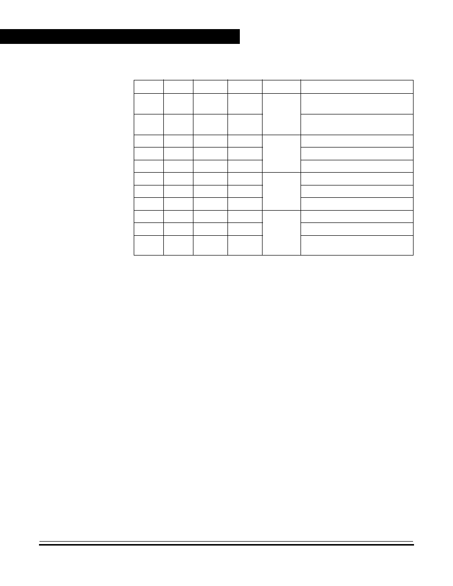
Timer Interface Module (TIM)
Advance Information
MC68HC(7)08KH12
--
Rev. 1.0
180
Timer Interface Module (TIM)
MOTOROLA
NOTE:
Before enabling a TIM channel register for input capture operation, make
sure that the PTEx/TCHx pin is stable for at least two bus clocks.
TOVx -- Toggle-On-Overflow Bit
When channel x is an output compare channel, this read/write bit
controls the behavior of the channel x output when the TIM counter
overflows. When channel x is an input capture channel, TOVx has no
effect. Reset clears the TOVx bit.
1 = Channel x pin toggles on TIM counter overflow.
0 = Channel x pin does not toggle on TIM counter overflow.
NOTE:
When TOVx is set, a TIM counter overflow takes precedence over a
channel x output compare if both occur at the same time.
CHxMAX -- Channel x Maximum Duty Cycle Bit
When the TOVx bit is at logic zero, setting the CHxMAX bit forces the
duty cycle of buffered and unbuffered PWM signals to 100%. As
Figure 11-7
shows, the CHxMAX bit takes effect in the cycle after it
is set or cleared. The output stays at the 100% duty cycle level until
the cycle after CHxMAX is cleared.
Table 11-3. Mode, Edge, and Level Selection
MSxB
MSxA
ELSxB
ELSxA
Mode
Configuration
X
0
0
0
Output
Preset
Pin under Port Control;
Initial Output Level High
X
1
0
0
Pin under Port Control;
Initial Output Level Low
0
0
0
1
Input
Capture
Capture on Rising Edge Only
0
0
1
0
Capture on Falling Edge Only
0
0
1
1
Capture on Rising or Falling Edge
0
1
0
1
Output
Compare
or PWM
Toggle Output on Compare
0
1
1
0
Clear Output on Compare
0
1
1
1
Set Output on Compare
1
X
0
1
Buffered
Output
Compare or
Buffered
PWM
Toggle Output on Compare
1
X
1
0
Clear Output on Compare
1
X
1
1
Set Output on Compare
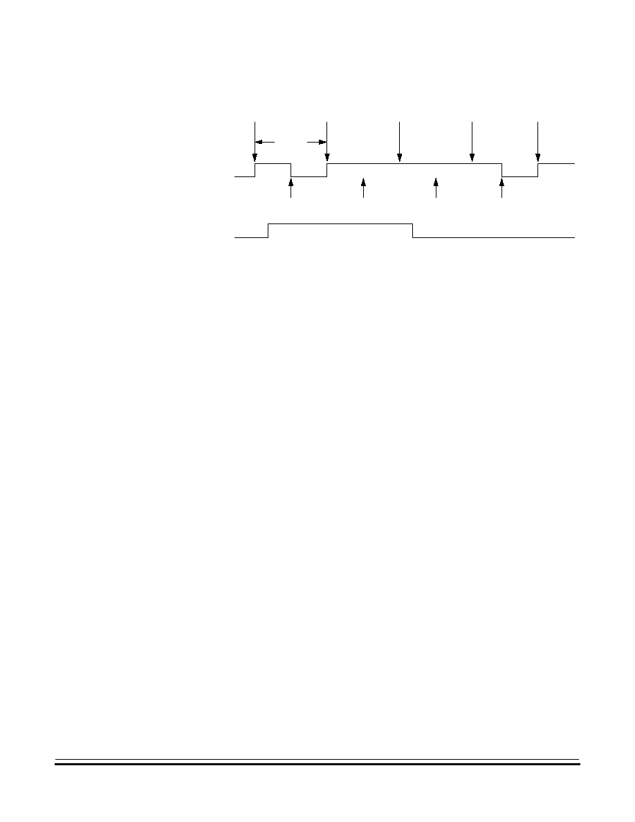
Timer Interface Module (TIM)
I/O Registers
MC68HC(7)08KH12
--
Rev. 1.0
Advance Information
MOTOROLA
Timer Interface Module (TIM)
181
Figure 11-7. CHxMAX Latency
11.9.5 TIM Channel Registers (TCH0H/L≠TCH1H/L)
These read/write registers contain the captured TIM counter value of the
input capture function or the output compare value of the output
compare function. The state of the TIM channel registers after reset is
unknown.
In input capture mode (MSxB:MSxA = 0:0), reading the high byte of the
TIM channel x registers (TCHxH) inhibits input captures until the low
byte (TCHxL) is read.
In output compare mode (MSxB:MSxA
0:0), writing to the high byte of
the TIM channel x registers (TCHxH) inhibits output compares until the
low byte (TCHxL) is written.
OUTPUT
OVERFLOW
PTEx/TCHx
PERIOD
CHxMAX
OVERFLOW
OVERFLOW
OVERFLOW
OVERFLOW
COMPARE
OUTPUT
COMPARE
OUTPUT
COMPARE
OUTPUT
COMPARE
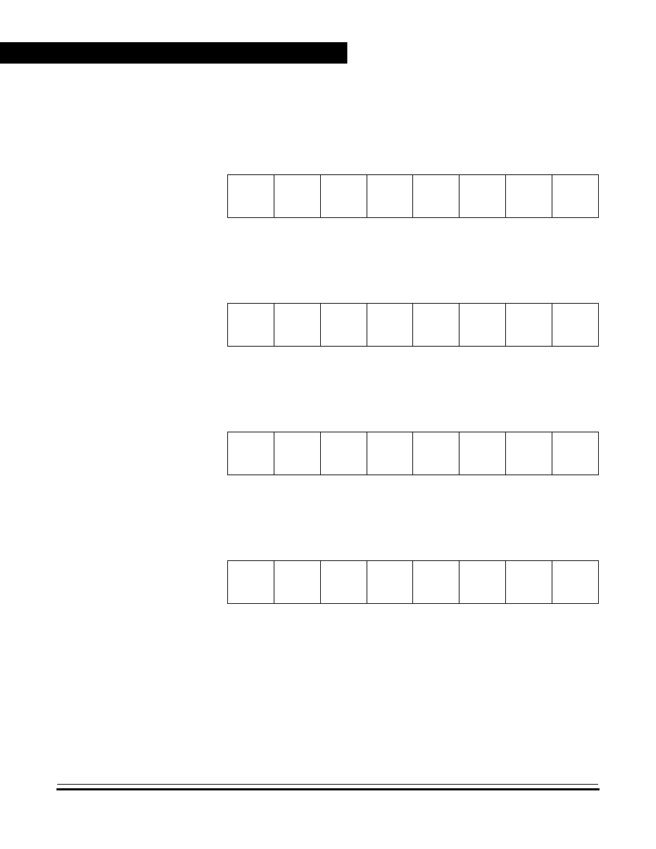
Timer Interface Module (TIM)
Advance Information
MC68HC(7)08KH12
--
Rev. 1.0
182
Timer Interface Module (TIM)
MOTOROLA
Address:
$0017
TCH0H
Bit 7
6
5
4
3
2
1
Bit 0
Read:
Bit15
Bit14
Bit13
Bit12
Bit11
Bit10
Bit9
Bit8
Write:
Reset:
Indeterminate after reset
Address:
$0018
TCH0L
Bit 7
6
5
4
3
2
1
Bit 0
Read:
Bit7
Bit6
Bit5
Bit4
Bit3
Bit2
Bit1
Bit0
Write:
Reset:
Indeterminate after reset
Address:
$001A
TCH1H
Bit 7
6
5
4
3
2
1
Bit 0
Read:
Bit15
Bit14
Bit13
Bit12
Bit11
Bit10
Bit9
Bit8
Write:
Reset:
Indeterminate after reset
Address:
$001B
TCH1L
Bit 7
6
5
4
3
2
1
Bit 0
Read:
Bit7
Bit6
Bit5
Bit4
Bit3
Bit2
Bit1
Bit0
Write:
Reset:
Indeterminate after reset
Figure 11-8. TIM Channel Registers (TCH0H/L:TCH1H/L)

MC68HC(7)08KH12
--
Rev. 1.0
Advance Information
MOTOROLA
I/O Ports
183
Advance Information -- MC68HC(7)08KH12
Section 12. I/O Ports
12.1 Contents
12.2
Introduction . . . . . . . . . . . . . . . . . . . . . . . . . . . . . . . . . . . . . . . 184
12.3
Port A . . . . . . . . . . . . . . . . . . . . . . . . . . . . . . . . . . . . . . . . . . . 186
12.3.1
Port A Data Register (PTA) . . . . . . . . . . . . . . . . . . . . . . . . 186
12.3.2
Data Direction Register A (DDRA) . . . . . . . . . . . . . . . . . . 186
12.4
Port B . . . . . . . . . . . . . . . . . . . . . . . . . . . . . . . . . . . . . . . . . . . 188
12.4.1
Port B Data Register (PTB) . . . . . . . . . . . . . . . . . . . . . . . . 188
12.4.2
Data Direction Register B (DDRB) . . . . . . . . . . . . . . . . . . 189
12.5
Port C . . . . . . . . . . . . . . . . . . . . . . . . . . . . . . . . . . . . . . . . . . . 190
12.5.1
Port C Data Register (PTC). . . . . . . . . . . . . . . . . . . . . . . . 190
12.5.2
Data Direction Register C (DDRC) . . . . . . . . . . . . . . . . . . 191
12.6
Port D . . . . . . . . . . . . . . . . . . . . . . . . . . . . . . . . . . . . . . . . . . . 192
12.6.1
Port D Data Register (PTD). . . . . . . . . . . . . . . . . . . . . . . . 193
12.6.2
Data Direction Register D (DDRD) . . . . . . . . . . . . . . . . . . 193
12.7
Port E . . . . . . . . . . . . . . . . . . . . . . . . . . . . . . . . . . . . . . . . . . . 195
12.7.1
Port E Data Register (PTE) . . . . . . . . . . . . . . . . . . . . . . . . 195
12.7.2
Data Direction Register E (DDRE) . . . . . . . . . . . . . . . . . . 196
12.7.3
Port-E Optical Interface Enable Register . . . . . . . . . . . . . 198
12.8
Port F . . . . . . . . . . . . . . . . . . . . . . . . . . . . . . . . . . . . . . . . . . . 202
12.8.1
Port F Data Register (PTF) . . . . . . . . . . . . . . . . . . . . . . . . 202
12.8.2
Data Direction Register F (DDRF). . . . . . . . . . . . . . . . . . . 203
12.9
Port Options . . . . . . . . . . . . . . . . . . . . . . . . . . . . . . . . . . . . . . 204
12.9.1
Port Option Control Register (POC) . . . . . . . . . . . . . . . . . 204
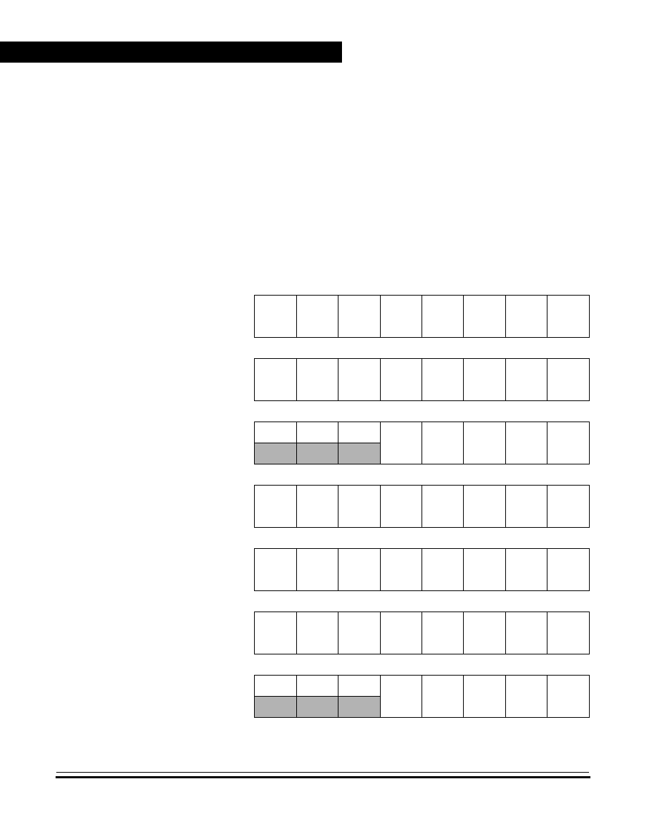
I/O Ports
Advance Information
MC68HC(7)08KH12
--
Rev. 1.0
184
I/O Ports
MOTOROLA
12.2 Introduction
Forty-two bidirectional input-output (I/O) pins form five parallel ports. All
I/O pins are programmable as inputs or outputs.
NOTE:
Connect any unused I/O pins to an appropriate logic level, either V
DD
or
V
SS
. Although the I/O ports do not require termination for proper
operation, termination reduces excess current consumption and the
possibility of electrostatic damage.
Table 12-1. I/O Port Register Summary
Addr.
Register Name
Bit 7
6
5
4
3
2
1
Bit 0
$0000
Port A Data Register
(PTA)
Read:
PTA7
PTA6
PTA5
PTA4
PTA3
PTA2
PTA1
PTA0
Write:
Reset:
Unaffected by reset
$0001
Port B Data Register
(PTB)
Read:
PTB7
PTB6
PTB5
PTB4
PTB3
PTB2
PTB1
PTB0
Write:
Reset:
Unaffected by reset
$0002
Port C Data Register
(PTC)
Read:
0
0
0
PTC4
PTC3
PTC2
PTC1
PTC0
Write:
Reset:
Unaffected by reset
$0003
Port D Data Register
(PTD)
Read:
PTD7
PTD6
PTD5
PTD4
PTD3
PTD2
PTD1
PTD0
Write:
Reset:
Unaffected by reset
$0004
Data Direction Register A
(DDRA)
Read:
DDRA7
DDRA6
DDRA5
DDRA4
DDRA3
DDRA2
DDRA1
DDRA0
Write:
Reset:
0
0
0
0
0
0
0
0
$0005
Data Direction Register B
(DDRB)
Read:
DDRB7
DDRB6
DDRB5
DDRB4
DDRB3
DDRB2
DDRB1
DDRB0
Write:
Reset:
0
0
0
0
0
0
0
0
$0006
Data Direction Register C
(DDRC)
Read:
0
0
0
DDRC4
DDRC3
DDRC2
DDRC1
DDRC0
Write:
Reset:
0
0
0
0
0
0
0
0
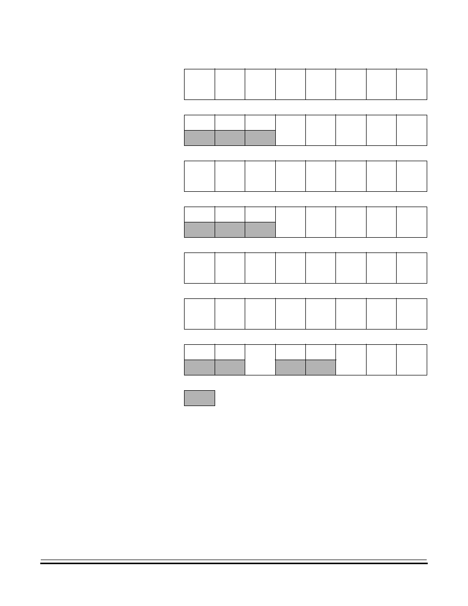
I/O Ports
Introduction
MC68HC(7)08KH12
--
Rev. 1.0
Advance Information
MOTOROLA
I/O Ports
185
$0007
Data Direction Register D
(DDRD)
Read:
DDRD7
DDRD6
DDRD5
DDRD4
DDRD3
DDRD2
DDRD1
DDRD0
Write:
Reset:
0
0
0
0
0
0
0
0
$0008
Port E Data Register
(PTE)
Read:
0
0
0
PTE4
PTE3
PTE2
PTE1
PTE0
Write:
Reset:
Unaffected by reset
$0009
Port F Data Register
(PTF)
Read:
PTF7
PTF6
PTF5
PTF4
PTF3
PTF2
PTF1
PTF0
Write:
Reset:
Unaffected by reset
$000A
Data Direction Register E
(DDRE)
Read:
0
0
0
DDRE4
DDRE3
DDRE2
DDRE1
DDRE0
Write:
Reset:
0
0
0
0
0
0
0
0
$000B
Data Direction Register F
(DDRF)
Read:
DDRF7
DDRF6
DDRF5
DDRF4
DDRF3
DDRF2
DDRF1
DDRF0
Write:
Reset:
0
0
0
0
0
0
0
0
$001C
Port E Optical Interface
Enable Register
(EOIER)
Read:
YREF2
YREF1
YREF0
XREF2
XREF1
XREF0
OIEY
OIEX
Write:
Reset:
0
1
0
0
1
0
0
0
$001D
Port Option Control
Register
(POC)
Read:
0
0
LDD
0
0
PCP
PBP
PAP
Write:
Reset:
0
0
1
0
0
0
0
0
= Unimplemented

I/O Ports
Advance Information
MC68HC(7)08KH12
--
Rev. 1.0
186
I/O Ports
MOTOROLA
12.3 Port A
Port A is an 8-bit general-purpose bidirectional I/O port with software
configurable pullups.
12.3.1 Port A Data Register (PTA)
The port A data register contains a data latch for each of the eight port
A pins.
PTA[7:0] -- Port A Data Bits
These read/write bits are software programmable. Data direction of
each port A pin is under the control of the corresponding bit in data
direction register A. Reset has no effect on port A data.
The port A pullup enable bit, PAP, in the port option control register
(POC) enables pullups on port A pins if the respective pin is configured
as an input.
(See 12.9 Port Options
.)
12.3.2 Data Direction Register A (DDRA)
Data direction register A determines whether each port A pin is an input
or an output. Writing a logic one to a DDRA bit enables the output buffer
for the corresponding port A pin; a logic zero disables the output buffer.
Address:
$0000
Bit 7
6
5
4
3
2
1
Bit 0
Read:
PTA7
PTA6
PTA5
PTA4
PTA3
PTA2
PTA1
PTA0
Write:
Reset:
Unaffected by reset
Figure 12-1. Port A Data Register (PTA)
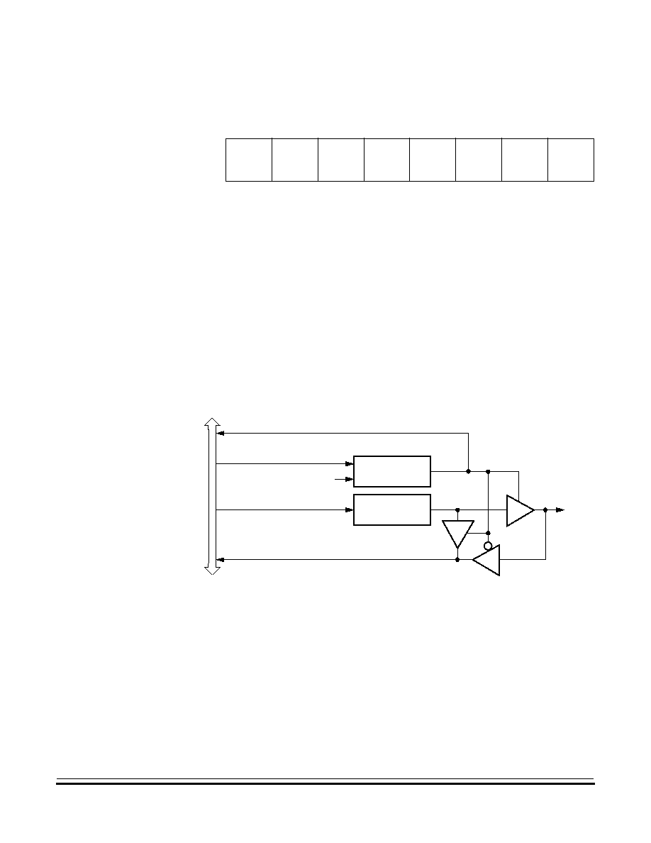
I/O Ports
Port A
MC68HC(7)08KH12
--
Rev. 1.0
Advance Information
MOTOROLA
I/O Ports
187
DDRA[7:0] -- Data Direction Register A Bits
These read/write bits control port A data direction. Reset clears
DDRA[7:0], configuring all port A pins as inputs.
1 = Corresponding port A pin configured as output
0 = Corresponding port A pin configured as input
NOTE:
Avoid glitches on port A pins by writing to the port A data register before
changing data direction register A bits from 0 to 1.
Figure 12-3
shows the port A I/O logic.
Figure 12-3. Port A I/O Circuit
When bit DDRAx is a logic one, reading address $0000 reads the PTAx
data latch. When bit DDRAx is a logic zero, reading address $0000
reads the voltage level on the pin. The data latch can always be written,
regardless of the state of its data direction bit.
Table 12-2
summarizes
the operation of the port A pins.
Address:
$0004
Bit 7
6
5
4
3
2
1
Bit 0
Read:
DDRA7
DDRA6
DDRA5
DDRA4
DDRA3
DDRA2
DDRA1
DDRA0
Write:
Reset:
0
0
0
0
0
0
0
0
Figure 12-2. Data Direction Register A (DDRA)
READ DDRA ($0004)
WRITE DDRA ($0004)
RESET
WRITE PTA ($0000)
READ PTA ($0000)
PTAx
DDRAx
PTAx
INTERNAL D
A
T
A
B
U
S

I/O Ports
Advance Information
MC68HC(7)08KH12
--
Rev. 1.0
188
I/O Ports
MOTOROLA
12.4 Port B
Port B is an 8-bit general-purpose bidirectional I/O port with software
configurable pullups.
12.4.1 Port B Data Register (PTB)
The port B data register contains a data latch for each of the eight port B
pins.
PTB[7:0] -- Port B Data Bits
These read/write bits are software-programmable. Data direction of
each port B pin is under the control of the corresponding bit in data
direction register B. Reset has no effect on port B data.
The port B pullup enable bit, PBP, in the port option control register
(POC) enables pullups on port B pins if the respective pin is configured
as an input.
(See 12.9 Port Options
.).
Table 12-2. Port A Pin Functions
DDRA
Bit
PTA Bit
I/O Pin
Mode
Accesses
to DDRA
Accesses to PTA
Read/Write
Read
Write
0
X
(1)
Input, Hi-Z
(2)
DDRA[7:0]
Pin
PTA[7:0]
(3)
1
X
Output
DDRA[7:0]
PTA[7:0]
PTA[7:0]
1. X = don't care
2. Hi-Z = high impedance
3. Writing affects data register, but does not affect input.
Address:
$0001
Bit 7
6
5
4
3
2
1
Bit 0
Read:
PTB7
PTB6
PTB5
PTB4
PTB3
PTB2
PTB1
PTB0
Write:
Reset:
Unaffected by reset
Figure 12-4. Port B Data Register (PTB)

I/O Ports
Port B
MC68HC(7)08KH12
--
Rev. 1.0
Advance Information
MOTOROLA
I/O Ports
189
12.4.2 Data Direction Register B (DDRB)
Data direction register B determines whether each port B pin is an input
or an output. Writing a logic one to a DDRB bit enables the output buffer
for the corresponding port B pin; a logic zero disables the output buffer.
DDRB[7:0] -- Data Direction Register B Bits
These read/write bits control port B data direction. Reset clears
DDRB[7:0], configuring all port B pins as inputs.
1 = Corresponding port B pin configured as output
0 = Corresponding port B pin configured as input
NOTE:
Avoid glitches on port B pins by writing to the port B data register before
changing data direction register B bits from 0 to 1.
Figure 12-6
shows the port B I/O logic.
Figure 12-6. Port B I/O Circuit
Address:
$0005
Bit 7
6
5
4
3
2
1
Bit 0
Read:
DDRB7
DDRB6
DDRB5
DDRB4
DDRB3
DDRB2
DDRB1
DDRB0
Write:
Reset:
0
0
0
0
0
0
0
0
Figure 12-5. Data Direction Register B (DDRB)
READ DDRB ($0005)
WRITE DDRB ($0005)
RESET
WRITE PTB ($0001)
READ PTB ($0001)
PTBx
DDRBx
PTBx
INTERNAL D
A
T
A
B
U
S
I/O Ports
Advance Information
MC68HC(7)08KH12
--
Rev. 1.0
190
I/O Ports
MOTOROLA
When bit DDRBx is a logic one, reading address $0001 reads the PTBx
data latch. When bit DDRBx is a logic zero, reading address $0001
reads the voltage level on the pin. The data latch can always be written,
regardless of the state of its data direction bit.
Table 12-3
summarizes
the operation of the port B pins.
12.5 Port C
Port C is a 5-bit general-purpose bidirectional I/O port with software
configurable pullups and current drive options.
12.5.1 Port C Data Register (PTC)
The port C data register contains a data latch for each of the five port C
pins.
Table 12-3. Port B Pin Functions
DDRB
Bit
PTB Bit
I/O Pin Mode
Accesses to
DDRB
Accesses to PTB
Read/Write
Read
Write
0
X
(1)
1. X = don't care
Input, Hi-Z
(2)
2. Hi-Z = high impedance
DDRB[7:0]
Pin
PTB[7:0]
(3)
3. Writing affects data register, but does not affect input.
1
X
Output
DDRB[7:0]
PTB[7:0]
PTB[7:0]
Address:
$0002
Bit 7
6
5
4
3
2
1
Bit 0
Read:
0
0
0
PTC4
PTC3
PTC2
PTC1
PTC0
Write:
Reset:
Unaffected by reset
= Unimplemented
Figure 12-7. Port C Data Register (PTC)

I/O Ports
Port C
MC68HC(7)08KH12
--
Rev. 1.0
Advance Information
MOTOROLA
I/O Ports
191
PTC[4:0] -- Port C Data Bits
These read/write bits are software-programmable. Data direction of
each port C pin is under the control of the corresponding bit in data
direction register C. Reset has no effect on port C data.
The port C pullup enable bit, PCP, in the port option control register
(POC) enables pullups on port C pins if the respective pin is configured
as an input.
(See 12.9 Port Options
.)
The LED direct drive bit, LDD, in the port option control register (POC)
controls the drive options for Port C.
12.5.2 Data Direction Register C (DDRC)
Data direction register C determines whether each port C pin is an input
or an output. Writing a logic one to a DDRC bit enables the output buffer
for the corresponding port C pin; a logic zero disables the output buffer.
DDRC[4:0] -- Data Direction Register C Bits
These read/write bits control port C data direction. Reset clears
DDRC[4:0], configuring all port C pins as inputs.
1 = Corresponding port C pin configured as output
0 = Corresponding port C pin configured as input
NOTE:
Avoid glitches on port C pins by writing to the port C data register before
changing data direction register C bits from 0 to 1.
Figure 12-9
shows the port C I/O logic.
Address:
$0006
Bit 7
6
5
4
3
2
1
Bit 0
Read:
0
0
0
DDRC4
DDRC3
DDRC2
DDRC1
DDRC0
Write:
Reset:
0
0
0
0
0
0
0
0
= Unimplemented
Figure 12-8. Data Direction Register C (DDRC)
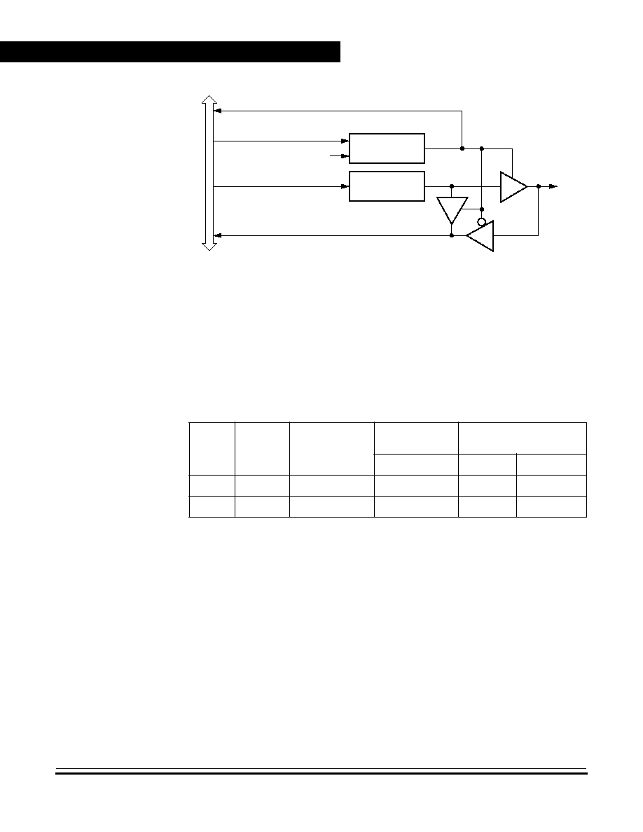
I/O Ports
Advance Information
MC68HC(7)08KH12
--
Rev. 1.0
192
I/O Ports
MOTOROLA
Figure 12-9. Port C I/O Circuit
When bit DDRCx is a logic one, reading address $0002 reads the PTCx
data latch. When bit DDRCx is a logic zero, reading address $0002
reads the voltage level on the pin. The data latch can always be written,
regardless of the state of its data direction bit.
Table 12-4
summarizes
the operation of the port C pins.
12.6 Port D
Port D is an 8-bit general-purpose bidirectional I/O port that shares its
pins with the keyboard interrupt module (KBI). All Port D pins have built-
in schmitt triggered input.
Table 12-4. Port C Pin Functions
DDRC
Bit
PTC Bit
I/O Pin Mode
Accesses to
DDRC
Accesses to PTC
Read/Write
Read
Write
0
X
(1)
1. X = don't care
Input, Hi-Z
(2)
2. Hi-Z = high impedance
DDRC[4:0]
Pin
PTC[4:0]
(3)
3. Writing affects data register, but does not affect input.
1
X
Output
DDRC[4:0]
PTC[4:0]
PTC[4:0]
READ DDRC ($0006)
WRITE DDRC ($0006)
RESET
WRITE PTC ($0002)
READ PTC ($0002)
PTCx
DDRCx
PTCx
INTERNAL D
A
T
A
B
U
S

I/O Ports
Port D
MC68HC(7)08KH12
--
Rev. 1.0
Advance Information
MOTOROLA
I/O Ports
193
12.6.1 Port D Data Register (PTD)
The port D data register contains a data latch for each of the eight port D
pins.
PTD[7:0] -- Port D Data Bits
These read/write bits are software programmable. Data direction of
each port D pin is under control of the corresponding bit in data
direction register D. Reset has no effect on port D data.
The port D pullups are automatically enabled if the respective pin is
configured as a keyboard interrupt. (See
15.4.1 Port-D Keyboard
Interrupt Functional Description
.)
The port-D keyboard interrupt enable bits, KBDIE7--KBDIE0, in the
port-D keyboard interrupt enable register (KBDIER), enable the port D
pins as external interrupt pins.
See Section 15. Keyboard Interrupt
Module (KBI)
.
12.6.2 Data Direction Register D (DDRD)
Data direction register D determines whether each port D pin is an input
or an output. Writing a logic one to a DDRD bit enables the output buffer
for the corresponding port D pin; a logic zero disables the output buffer.
Address:
$0003
Bit 7
6
5
4
3
2
1
Bit 0
Read:
PTD7
PTD6
PTD5
PTD4
PTD3
PTD2
PTD1
PTD0
Write:
Reset:
Unaffected by reset
Alternate
Function:
KBD7
KBD6
KBD5
KBD4
KBD3
KBD2
KBD1
KBD0
Figure 12-10. Port D Data Register (PTD)
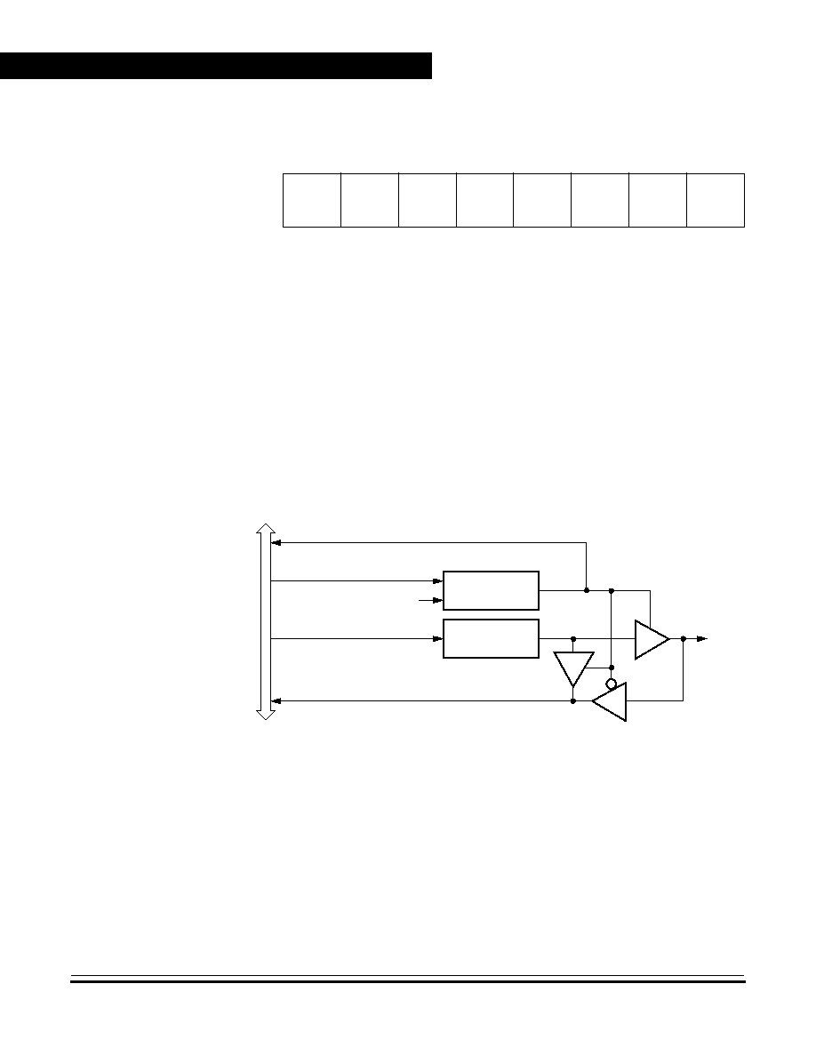
I/O Ports
Advance Information
MC68HC(7)08KH12
--
Rev. 1.0
194
I/O Ports
MOTOROLA
DDRD[7:0] -- Data Direction Register D Bits
These read/write bits control port D data direction. Reset clears
DDRD[7:0], configuring all port D pins as inputs.
1 = Corresponding port D pin configured as output
0 = Corresponding port D pin configured as input
NOTE:
Avoid glitches on port D pins by writing to the port D data register before
changing data direction register D bits from 0 to 1.
Figure 12-12
shows the port D I/O logic.
Figure 12-12. Port D I/O Circuit
When bit DDRDx is a logic one, reading address $0003 reads the PTDx
data latch. When bit DDRDx is a logic zero, reading address $0003
reads the voltage level on the pin. The data latch can always be written,
regardless of the state of its data direction bit.
Table 12-5
summarizes
the operation of the port D pins.
Address:
$0007
Bit 7
6
5
4
3
2
1
Bit 0
Read:
DDRD7
DDRD6
DDRD5
DDRD4
DDRD3
DDRD2
DDRD1
DDRD0
Write:
Reset:
0
0
0
0
0
0
0
0
Figure 12-11. Data Direction Register D (DDRD)
READ DDRD ($0007)
WRITE DDRD ($0007)
RESET
WRITE PTD ($0003)
READ PTD ($0003)
PTDx
DDRDx
PTDx
INTERNAL D
A
T
A
B
U
S
I/O Ports
Port E
MC68HC(7)08KH12
--
Rev. 1.0
Advance Information
MOTOROLA
I/O Ports
195
12.7 Port E
Port E is a 5-bit special function port that shares four of its pins with the
keyboard interrupt module (KBI) and shares three of its pins with the
timer interface module (TIM). PTE3≠PTE0 pins have built-in schmitt
triggered input and software configurable pull-up; In addition,
PTE3≠PTE0 pins have built-in optical interface circuit which can be
enabled via the Port-E Optical Interface Enable Register.
12.7.1 Port E Data Register (PTE)
The port E data register contains a data latch for each of the five port E
pins.
Table 12-5. Port D Pin Functions
DDRD
Bit
PTD Bit
I/O Pin Mode
Accesses to
DDRD
Accesses to PTD
Read/Write
Read
Write
0
X
(1)
Input, Hi-Z
(2)
DDRD[7:0]
Pin
PTD[7:0]
(3)
1
X
Output
DDRD[7:0]
PTD[7:0]
PTD[7:0]
1. X = don't care
2. Hi-Z = high impedance
3. Writing affects data register, but does not affect input.
Address:
$0008
Bit 7
6
5
4
3
2
1
Bit 0
Read:
0
0
0
PTE4
PTE3
PTE2
PTE1
PTE0
Write:
Reset:
Unaffected by reset
= Unimplemented
Alternate
Function:
KBE3
KBE2
KBE1
KBE0
Alternate
Function:
TCH1
TCH0
TCLK
Figure 12-13. Port E Data Register (PTE)

I/O Ports
Advance Information
MC68HC(7)08KH12
--
Rev. 1.0
196
I/O Ports
MOTOROLA
PTE[4:0] -- Port E Data Bits
PTE[4:0] are read/write, software-programmable bits. Data direction
of each port E pin is under the control of the corresponding bit in data
direction register E.
TCH1-TCH0 -- Timer Channel I/O Bits
The PTE2/TCH1-PTE1/TCH0 pins are the TIM input capture/output
compare pins. The edge/level select bits, ELSxB and ELSxA,
determine whether the PTE2/TCH1≠PTE1/TCH0 pins are timer
channel I/O pins or general-purpose I/O pins.
See Section 11. Timer
Interface Module (TIM)
.
NOTE:
Data direction register E (DDRE) does not affect the data direction of
port E pins that are being used by the TIM. However, the DDRE bits
always determine whether reading port E returns the states of the
latches or the states of the pins.
TCLK -- Timer Clock Input
The PTE0/TCLK pin is the external clock input for the TIM. The
prescaler select bits, PS2-PS0, selects PE0/TCLK as the TIM clock
input. When not selected as the TIM clock, PE0/TCLK is available for
general purpose I/O.
See Section 11. Timer Interface Module (TIM)
.
The PEPE[3:0] bits in the port E keyboard interrupt enable register
enable individual pull-ups on port E pins PTE3≠PTE0 if the respective
pin is configured as an input.
(See 15.5.3.2 Port-E Keyboard Interrupt
Enable Register
.)
The port-E keyboard interrupt enable bits, KBEIE3--KBEIE0, in the port-
E keyboard interrupt enable register (KBEIER), enable the port E pins as
external interrupt pins.
See Section 15. Keyboard Interrupt Module
(KBI)
.
12.7.2 Data Direction Register E (DDRE)
Data direction register E determines whether each port E pin is an input
or an output. Writing a logic one to a DDRE bit enables the output buffer
for the corresponding port E pin; a logic zero disables the output buffer.
I/O Ports
Port E
MC68HC(7)08KH12
--
Rev. 1.0
Advance Information
MOTOROLA
I/O Ports
197
DDRE[4:0] -- Data Direction Register E Bits
These read/write bits control port E data direction. Reset clears
DDRE[4:0], configuring all port E pins as inputs.
1 = Corresponding port E pin configured as output
0 = Corresponding port E pin configured as input
NOTE:
Avoid glitches on port E pins by writing to the port E data register before
changing data direction register E bits from 0 to 1.
Figure 12-15
shows the port E I/O logic.
Figure 12-15. Port E I/O Circuit
When bit DDREx is a logic one, reading address $0008 reads the PTEx
data latch. When bit DDREx is a logic zero, reading address $0008
reads the voltage level on the pin. The data latch can always be written,
regardless of the state of its data direction bit.
Table 12-4
summarizes
the operation of the port E pins.
Address:
$000A
Bit 7
6
5
4
3
2
1
Bit 0
Read:
0
0
0
DDRE4
DDRE3
DDRE2
DDRE1
DDRE0
Write:
Reset:
0
0
0
0
0
0
0
0
= Unimplemented
Figure 12-14. Data Direction Register E (DDRE)
READ DDRE ($000A)
WRITE DDRE ($000A)
RESET
WRITE PTE ($0008)
READ PTE ($0008)
PTEx
DDREx
PTEx
INTERNAL D
A
T
A
B
U
S
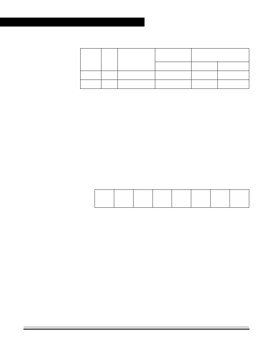
I/O Ports
Advance Information
MC68HC(7)08KH12
--
Rev. 1.0
198
I/O Ports
MOTOROLA
12.7.3 Port-E Optical Interface Enable Register
Port E pins PTE3≠PTE0, each has an optical coupling interface circuit
which is specially built for optical mouse application. Bits [1:0] of the
Optical Interface Enable register enable or disable the interface circuit in
each port E pins PTE3≠PTE0, whilst bits [7:2] define the reference level
for the optical interface circuit for optimum performance.
OIEX -- Optical Interface Enable X.
This enables optical interface on PTE0 and PTE1 pins. It also enables
the voltage divider circuit.
1 = PTE0 and PTE1 optical interface enabled.
0 = PTE0 and PTE1 optical interface disabled.
OIEY -- Optical Interface Enable Y.
This enables optical interface on PTE2 and PTE3 pins. It also enables
the voltage divider circuit.
1 = PTE2 and PTE3 optical interface enabled.
0 = PTE2 and PTE3 optical interface disabled.
Table 12-6. Port E Pin Functions
DDRE
Bit
PTE
Bit
I/O Pin Mode
Accesses to
DDRE
Accesses to PTE
Read/Write
Read
Write
0
X
(1)
Input, Hi-Z
(2)
DDRE[4:0]
Pin
PTE[4:0]
(3)
1
X
Output
DDRE[4:0]
PTE[4:0]
PTE[4:0]
1. X = don't care
2. Hi-Z = high impedance
3. Writing affects data register, but does not affect input.
Address:
$001C
Bit 7
6
5
4
3
2
1
Bit 0
Read:
YREF2
YREF1
YREF0
XREF2
XREF1
XREF0
OIEY
OIEX
Write:
Reset:
0
1
0
0
1
0
0
0
Figure 12-16. Optical Interface Enable Register E (EOIER)

I/O Ports
Port E
MC68HC(7)08KH12
--
Rev. 1.0
Advance Information
MOTOROLA
I/O Ports
199
XREF2≠XREF0 -- Reference Voltage Selection X
These bits sets the slicing reference voltage for optical interface
associated with PTE0 and PTE1.
YREF2≠YREF0 -- Reference Voltage Selection Y
These bits sets the slicing reference voltage for optical interface
associated with PTE2 and PTE3.
XREF[2:0] / YREF[2:0]
PTE0-PTE1 / PTE2-PTE3
Reference Voltage (mV)
0
200
1
300
2
400
3
500
4
600
5
700
6
800
7
900
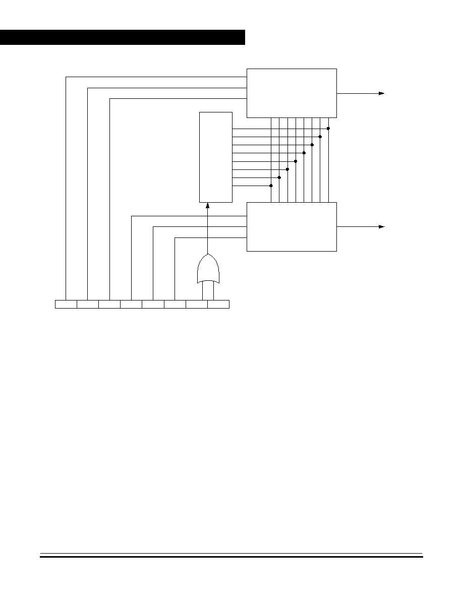
I/O Ports
Advance Information
MC68HC(7)08KH12
--
Rev. 1.0
200
I/O Ports
MOTOROLA
Figure 12-17. Optical Interface Voltage References
X-VREF
VOLTAGE DIVIDER
ENABLE
VOLTAGE SELECTOR
Y-VREF
VOLTAGE SELECTOR
Y - REFERENCE
X - REFERENCE
YREF2 YREF1 YREF0 XREF2 XREF1 XREF0 OIEY
OIEX
OPTICAL INTERFACE REGISTER ($001C)
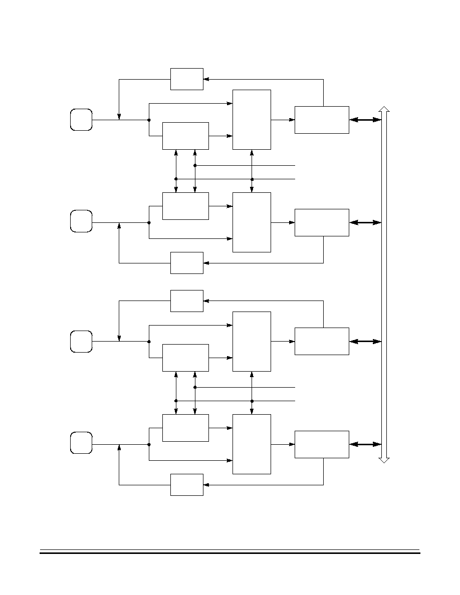
I/O Ports
Port E
MC68HC(7)08KH12
--
Rev. 1.0
Advance Information
MOTOROLA
I/O Ports
201
Figure 12-18. Port E Optical Coupling Interface
PTE0
PORT LOGIC
PTE0
OPTICAL
INTERFACE
OUTPUT
BUFFER
MUX
SELECT
PTE1
PORT LOGIC
PTE1
OPTICAL
INTERFACE
OUTPUT
BUFFER
X-VREF
OIEX (BIT0 OF $1C)
0
1
MUX
SELECT
0
1
INTERNAL D
A
T
A
B
U
S
PTE2
PORT LOGIC
PTE2
OPTICAL
INTERFACE
OUTPUT
BUFFER
MUX
SELECT
PTE3
PORT LOGIC
PTE3
OPTICAL
INTERFACE
OUTPUT
BUFFER
Y-VREF
OIEY (BIT1 OF $1C)
0
1
MUX
SELECT
0
1

I/O Ports
Advance Information
MC68HC(7)08KH12
--
Rev. 1.0
202
I/O Ports
MOTOROLA
12.8 Port F
Port F is an 8-bit general-purpose bidirectional I/O port that shares its
pins with the keyboard interrupt module (KBI). All Port F pins have built-
in schmitt triggered input and software configurable pull-up.
12.8.1 Port F Data Register (PTF)
The port F data register contains a data latch for each of the eight port F
pins.
PTF[7:0] -- Port F Data Bits
These read/write bits are software programmable. Data direction of
each port F pin is under the control of the corresponding bit in data
direction register F. Reset has no effect on port F data.
The port-F keyboard interrupt enable bits, KBFIE7--KBFIE0, in the
port-F keyboard interrupt enable register (KBFIER), enable the port F
pins as external interrupt pins.
See Section 15. Keyboard Interrupt
Module (KBI)
.
The PFPE[7:0] bits in the port F keyboard pull-up enable register enable
individual pull-ups on port F pins if the respective pin is configured as an
input.
(See 15.6.3.3 Port-F Pull-up Enable Register
.)
Address:
$0009
Bit 7
6
5
4
3
2
1
Bit 0
Read:
PTF7
PTF6
PTF5
PTF4
PTF3
PTF2
PTF1
PTF0
Write:
Reset:
Unaffected by reset
Alternate
Function:
KBF7
KBF6
KBF5
KBF4
KBF3
KBF2
KBF1
KBF0
Figure 12-19. Port F Data Register (PTF)
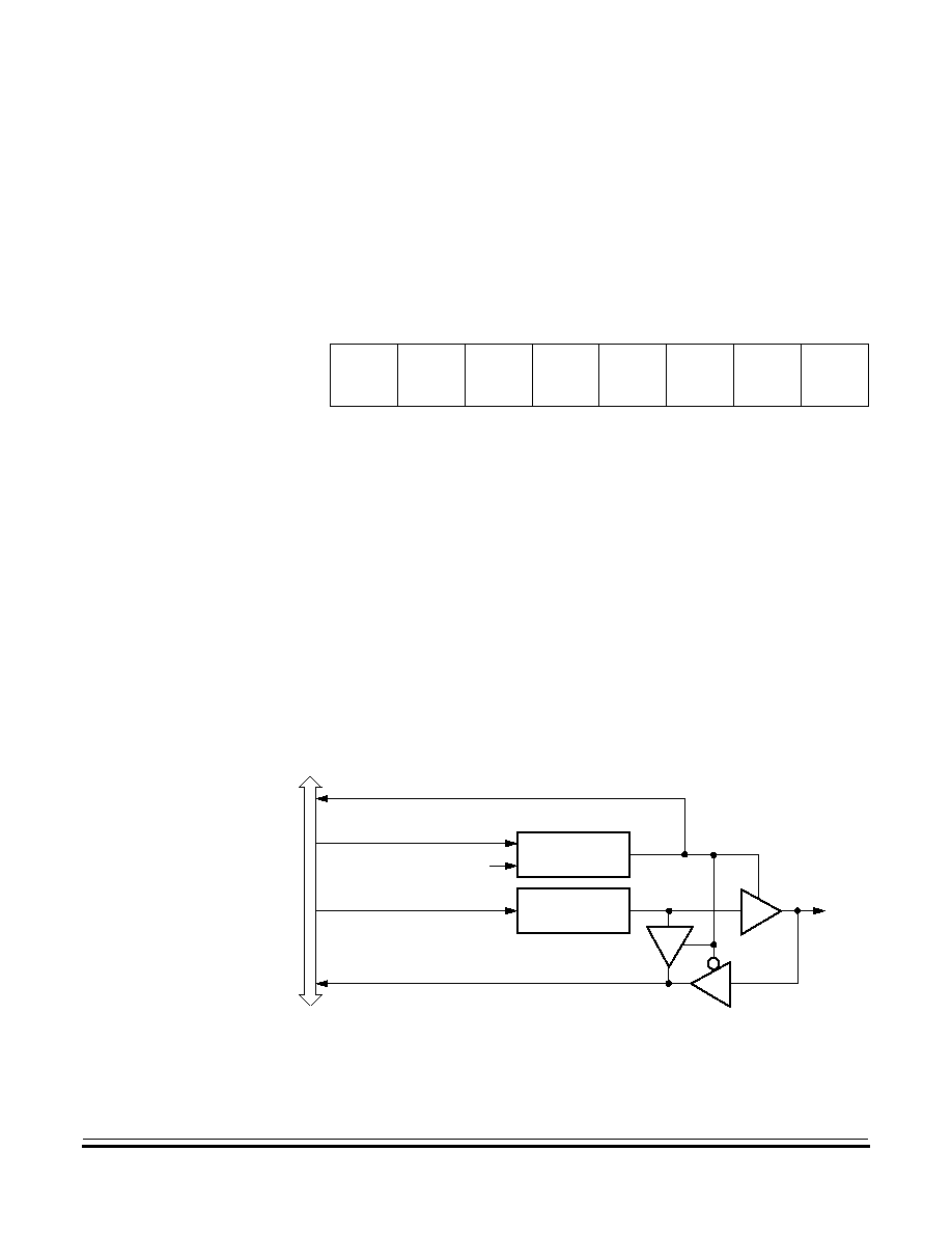
I/O Ports
Port F
MC68HC(7)08KH12
--
Rev. 1.0
Advance Information
MOTOROLA
I/O Ports
203
12.8.2 Data Direction Register F (DDRF)
Data direction register F determines whether each port F pin is an input
or an output. Writing a logic one to a DDRF bit enables the output buffer
for the corresponding port F pin; a logic zero disables the output buffer.
DDRF[7:0] -- Data Direction Register F Bits
These read/write bits control port F data direction. Reset clears
DDRF[7:0], configuring all port F pins as inputs.
1 = Corresponding port F pin configured as output
0 = Corresponding port F pin configured as input
NOTE:
Avoid glitches on port F pins by writing to the port F data register before
changing data direction register F bits from 0 to 1.
Figure 12-3
shows the port F I/O logic.
Figure 12-21. Port F I/O Circuit
Address:
$000B
Bit 7
6
5
4
3
2
1
Bit 0
Read:
DDRF7
DDRF6
DDRF5
DDRF4
DDRF3
DDRF2
DDRF1
DDRF0
Write:
Reset:
0
0
0
0
0
0
0
0
Figure 12-20. Data Direction Register F (DDRF)
READ DDRF ($000B)
WRITE DDRF ($000B)
RESET
WRITE PTF ($0009)
READ PTF ($0009)
PTFx
DDRFx
PTFx
INTERNAL D
A
T
A
B
U
S
I/O Ports
Advance Information
MC68HC(7)08KH12
--
Rev. 1.0
204
I/O Ports
MOTOROLA
When bit DDRFx is a logic one, reading address $0009 reads the PTFx
data latch. When bit DDRFx is a logic zero, reading address $0009
reads the voltage level on the pin. The data latch can always be written,
regardless of the state of its data direction bit.
Table 12-7
summarizes
the operation of the port F pins.
12.9 Port Options
All pins of port A, port B and port C have programmable pullup resistors.
Port C also has LED drive capability.
12.9.1 Port Option Control Register (POC)
The pullup option for each port is controlled by one bit in the port option
control register. One bit controls the LED drive configuration on port C.
Table 12-7. Port F Pin Functions
DDRE
Bit
PTE
Bit
I/O Pin Mode
Accesses to
DDRE
Accesses to PTE
Read/Write
Read
Write
0
X
(1)
1. X = don't care
Input, Hi-Z
(2)
2. Hi-Z = high impedance
DDRF[7:0]
Pin
PTF[7:0]
(3)
3. Writing affects data register, but does not affect input.
1
X
Output
DDRF[7:0]
PTF[7:0]
PTF[7:0]
Address:
$001D
Bit 7
6
5
4
3
2
1
Bit 0
Read:
0
0
LDD
0
0
PCP
PBP
PAP
Write:
Reset:
0
0
1
0
0
0
0
0
= Unimplemented
Figure 12-22. Port Option Control Register (POC)

I/O Ports
Port Options
MC68HC(7)08KH12
--
Rev. 1.0
Advance Information
MOTOROLA
I/O Ports
205
LDD -- LED Direct Drive Control
This read/write bit controls the output current capability of port C.
When set, the port C pins have current limiting ability so that a LED
can be connected directly between the port pin and V
DD
or V
SS
without the need of a series resistor.
1 = When respective port is configured as an output, make port C
become current limiting 3 mA source/10 mA sink port pins
0 = Configure port C to become standard I/O port pins
PCP -- Port C Pullup Enable
This read/write bit controls the pullup option for port C[7:0] if its
respective port pin is configured as an input.
1 = Configure port C to have internal pullups
0 = Disconnect port C internal pullups
PBP -- Port B Pullup Enable
This read/write bit controls the pullup option for the eight bits of port B
if its respective port pin is configured as an input.
1 = Configure port B to have internal pullups
0 = Disconnect port B internal pullups
PAP -- Port A Pullup Enable
This read/write bit controls the pullup option for the eight bits of port A
if its respective port pin is configured as an input.
1 = Configure port A to have internal pullups
0 = Disconnect port A internal pullups

I/O Ports
Advance Information
MC68HC(7)08KH12
--
Rev. 1.0
206
I/O Ports
MOTOROLA

MC68HC(7)08KH12
--
Rev. 1.0
Advance Information
MOTOROLA
Computer Operating Properly (COP)
207
Advance Information -- MC68HC(7)08KH12
Section 13. Computer Operating Properly (COP)
13.1 Contents
13.2
Introduction . . . . . . . . . . . . . . . . . . . . . . . . . . . . . . . . . . . . . . . 207
13.3
Functional Description . . . . . . . . . . . . . . . . . . . . . . . . . . . . . . 208
13.4
I/O Signals . . . . . . . . . . . . . . . . . . . . . . . . . . . . . . . . . . . . . . . 209
13.4.1
CGMXCLK. . . . . . . . . . . . . . . . . . . . . . . . . . . . . . . . . . . . . 209
13.4.2
COPCTL Write . . . . . . . . . . . . . . . . . . . . . . . . . . . . . . . . . 209
13.4.3
Power-On Reset . . . . . . . . . . . . . . . . . . . . . . . . . . . . . . . . 210
13.4.4
Internal Reset . . . . . . . . . . . . . . . . . . . . . . . . . . . . . . . . . . 210
13.4.5
Reset Vector Fetch . . . . . . . . . . . . . . . . . . . . . . . . . . . . . . 210
13.4.6
COPD (COP Disable) . . . . . . . . . . . . . . . . . . . . . . . . . . . . 210
13.4.7
COPRS (COP Rate Select). . . . . . . . . . . . . . . . . . . . . . . . 210
13.5
COP Control Register (COPCTL) . . . . . . . . . . . . . . . . . . . . . . 211
13.6
Interrupts. . . . . . . . . . . . . . . . . . . . . . . . . . . . . . . . . . . . . . . . . 211
13.7
Monitor Mode . . . . . . . . . . . . . . . . . . . . . . . . . . . . . . . . . . . . . 211
13.8
Low-Power Modes . . . . . . . . . . . . . . . . . . . . . . . . . . . . . . . . . 212
13.8.1
Wait Mode . . . . . . . . . . . . . . . . . . . . . . . . . . . . . . . . . . . . . 212
13.8.2
Stop Mode . . . . . . . . . . . . . . . . . . . . . . . . . . . . . . . . . . . . . 212
13.9
COP Module During Break Mode . . . . . . . . . . . . . . . . . . . . . . 212
13.2 Introduction
This section describes the computer operating properly module, a free-
running counter that generates a reset if allowed to overflow. The COP
module helps software recover from runaway code. Prevent a COP reset
by periodically clearing the COP counter.
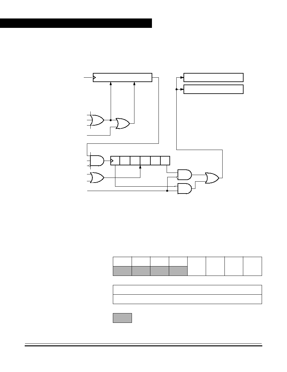
Computer Operating Properly (COP)
Advance Information
MC68HC(7)08KH12
--
Rev. 1.0
208
Computer Operating Properly (COP)
MOTOROLA
13.3 Functional Description
Figure 13-1
shows the structure of the COP module.
Figure 13-1. COP Block Diagram
COPCTL WRITE
CGMXCLK
RESET VECTOR FETCH
RESET CIRCUIT
RESET STATUS REGISTER
INTERNAL RESET SOURCES
12-BIT SIM COUNTER
CLEAR ALL STAGES
6-BIT COP COUNTER
COP DISABLE
RESET
COPCTL WRITE
CLEAR
COP MODULE
COPEN (FROM SIM)
COP COUNTER
COP CLOCK
COP TIMEOUT
STOP INSTRUCTION
(COPD FROM CONFIG)
COP RATE SEL
(COPRS FROM CONFIG)
CLEAR STAGES 5≠12
Table 13-1. COP I/O Port Register Summary
Addr.
Register Name
Bit 7
6
5
4
3
2
1
Bit 0
$001F
Configuration Register
(CONFIG)
Read:
0
0
0
0
SSREC
COPRS
STOP
COPD
Write:
Reset:
0
0
0
0
0
0
0
0
$FFFF
COP Control Register
(COPCTL)
Read:
Low byte of reset vector
Write:
Clear COP counter
Reset:
Unaffected by reset
One-time writable register
= Unimplemented

Computer Operating Properly (COP)
I/O Signals
MC68HC(7)08KH12
--
Rev. 1.0
Advance Information
MOTOROLA
Computer Operating Properly (COP)
209
The COP counter is a free-running 6-bit counter preceded by the 12-bit
SIM counter. If not cleared by software, the COP counter overflows and
generates an asynchronous reset after 2
18
≠ 2
4
or 2
13
≠ 2
4
CGMXCLK
cycles, depending on the setting of the COP rate select bit, COPRS, in
the configuration register. With a 2
18
≠ 2
4
CGMXCLK cycle overflow
option, a 6MHz crystal gives a COP timeout period of 43.688ms. Writing
any value to location $FFFF before an overflow occurs prevents a COP
reset by clearing the COP counter and stages 12 through 5 of the SIM
counter.
NOTE:
Service the COP immediately after reset and before entering or after
exiting stop mode to guarantee the maximum time before the first COP
counter overflow.
A COP reset pulls the RST pin low for 32 CGMXCLK cycles and sets the
COP bit in the reset status register (RSR)
(see 7.8.2 Reset Status
Register (RSR)
).
NOTE:
Place COP clearing instructions in the main program and not in an
interrupt subroutine. Such an interrupt subroutine could keep the COP
from generating a reset even while the main program is not working
properly.
13.4 I/O Signals
The following paragraphs describe the signals shown in
Figure 13-1
.
13.4.1 CGMXCLK
CGMXCLK is the crystal oscillator output signal. CGMXCLK frequency
is equal to the crystal frequency.
13.4.2 COPCTL Write
Writing any value to the COP control register (COPCTL)
(see 13.5 COP
Control Register (COPCTL)
) clears the COP counter and clears bits 12
through 4 of the SIM counter. Reading the COP control register returns
the low byte of the reset vector.

Computer Operating Properly (COP)
Advance Information
MC68HC(7)08KH12
--
Rev. 1.0
210
Computer Operating Properly (COP)
MOTOROLA
13.4.3 Power-On Reset
The power-on reset (POR) circuit in the SIM clears the SIM counter 4096
CGMXCLK cycles after power-up.
13.4.4 Internal Reset
An internal reset clears the SIM counter and the COP counter.
13.4.5 Reset Vector Fetch
A reset vector fetch occurs when the vector address appears on the data
bus. A reset vector fetch clears the SIM counter.
13.4.6 COPD (COP Disable)
The COPD signal reflects the state of the COP disable bit (COPD) in the
configuration register (CONFIG). (See
Figure 13-2 . Configuration
Register (CONFIG)
.)
13.4.7 COPRS (COP Rate Select)
The COPRS signal reflects the state of the COP rate select bit (COPRS)
in the configuration register. (See
Figure 13-2 . Configuration Register
(CONFIG)
.)
Address:
$001F
Bit 7
6
5
4
3
2
1
Bit 0
Read:
0
0
0
0
SSREC
COPRS
STOP
COPD
Write:
Reset:
0
0
0
0
0
0
0
0
= Unimplemented
This is a write-once after reset register.
(See
Section 5. Configuration Register (CONFIG)
.)
Figure 13-2. Configuration Register (CONFIG)

Computer Operating Properly (COP)
COP Control Register (COPCTL)
MC68HC(7)08KH12
--
Rev. 1.0
Advance Information
MOTOROLA
Computer Operating Properly (COP)
211
COPRS -- COP Rate Select Bit
COPRS selects the COP timeout period. Reset clears COPRS.
1 = COP reset cycle is (2
13
≠2
4
)
◊
CGMXCLK
0 = COP reset cycle is (2
18
≠2
4
)
◊
CGMXCLK
COPD -- COP Disable Bit
COPD disables the COP module.
1 = COP module disabled
0 = COP module enabled
13.5 COP Control Register (COPCTL)
The COP control register is located at address $FFFF and overlaps the
reset vector. Writing any value to $FFFF clears the COP counter and
starts a new timeout period. Reading location $FFFF returns the low
byte of the reset vector.
13.6 Interrupts
The COP does not generate CPU interrupt requests.
13.7 Monitor Mode
The COP is disabled in monitor mode when V
DD
+ V
HI
is present on the
IRQ1/V
PP
pin or on the RST pin.
Address:
$FFFF
Bit 7
6
5
4
3
2
1
Bit 0
Read:
Low byte of reset vector
Write:
Clear COP counter
Reset:
Unaffected by reset
Figure 13-3. COP Control Register (COPCTL)

Computer Operating Properly (COP)
Advance Information
MC68HC(7)08KH12
--
Rev. 1.0
212
Computer Operating Properly (COP)
MOTOROLA
13.8 Low-Power Modes
The WAIT and STOP instructions put the MCU in low-power
consumption standby modes.
13.8.1 Wait Mode
The COP continues to operate during wait mode. To prevent a COP
reset during wait mode, periodically clear the COP counter in a CPU
interrupt routine.
13.8.2 Stop Mode
Stop mode turns off the CGMXCLK input to the COP and clears the SIM
counter. Service the COP immediately before entering or after exiting
stop mode to ensure a full COP timeout period after entering or exiting
stop mode.
13.9 COP Module During Break Mode
The COP is disabled during a break interrupt when V
DD
+ V
HI
is present
on the RST pin.

MC68HC(7)08KH12
--
Rev. 1.0
Advance Information
MOTOROLA
External Interrupt (IRQ)
213
Advance Information -- MC68HC(7)08KH12
Section 14. External Interrupt (IRQ)
14.1 Contents
14.2
Introduction . . . . . . . . . . . . . . . . . . . . . . . . . . . . . . . . . . . . . . . 213
14.3
Features . . . . . . . . . . . . . . . . . . . . . . . . . . . . . . . . . . . . . . . . . 213
14.4
Functional Description . . . . . . . . . . . . . . . . . . . . . . . . . . . . . . 214
14.4.1
IRQ1/V
PP
Pin . . . . . . . . . . . . . . . . . . . . . . . . . . . . . . . . . . . 215
14.5
IRQ Module During Break Interrupts . . . . . . . . . . . . . . . . . . . 217
14.6
IRQ Status and Control Register (ISCR) . . . . . . . . . . . . . . . . 217
14.2 Introduction
The IRQ module provides a non-maskable interrupt input.
14.3 Features
Features of the IRQ module include the following:
∑
A Dedicated External Interrupt Pin (IRQ1/V
PP
)
∑
IRQ1 Interrupt Control Bits
∑
Hysteresis Buffer
∑
Programmable Edge-only or Edge and Level Interrupt Sensitivity
∑
Automatic Interrupt Acknowledge
∑
IRQ1/V
PP
pin includes internal pullup resistor

External Interrupt (IRQ)
Advance Information
MC68HC(7)08KH12
--
Rev. 1.0
214
External Interrupt (IRQ)
MOTOROLA
14.4 Functional Description
A logic zero applied to the external interrupt pin can latch a CPU interrupt
request.
Figure 14-1
shows the structure of the IRQ module.
Interrupt signals on the IRQ1/V
PP
pin are latched into the IRQ1 latch. An
interrupt latch remains set until one of the following actions occurs:
∑
Vector fetch -- A vector fetch automatically generates an interrupt
acknowledge signal that clears the IRQ latch.
∑
Software clear -- Software can clear the interrupt latch by writing
to the acknowledge bit in the interrupt status and control register
(ISCR). Writing a logic one to the ACK1 bit clears the IRQ1 latch.
∑
Reset -- A reset automatically clears the interrupt latch.
The external interrupt pin is falling-edge-triggered and is software-
configurable to be either falling-edge or low-level-triggered. The MODE1
bit in the ISCR controls the triggering sensitivity of the IRQ1/V
PP
pin.
When the interrupt pin is edge-triggered only, the CPU interrupt request
remains set until a vector fetch, software clear, or reset occurs.
When the interrupt pin is both falling-edge and low-level-triggered, the
CPU interrupt request remains set until both of the following occur:
∑
Vector fetch or software clear
∑
Return of the interrupt pin to logic one
The vector fetch or software clear may occur before or after the interrupt
pin returns to logic one. As long as the pin is low, the interrupt request
remains pending. A reset will clear the latch and the MODE1 control bit,
thereby clearing the interrupt even if the pin stays low.
When set, the IMASK1 bit in the ISCR mask all external interrupt
requests. A latched interrupt request is not presented to the interrupt
priority logic unless the IMASK1 bit is clear.
NOTE:
The interrupt mask (I) in the condition code register (CCR) masks all
interrupt requests, including external interrupt requests.
(See 7.6
Exception Control
.)

External Interrupt (IRQ)
Functional Description
MC68HC(7)08KH12
--
Rev. 1.0
Advance Information
MOTOROLA
External Interrupt (IRQ)
215
Figure 14-1. IRQ Module Block Diagram
14.4.1 IRQ1/V
PP
Pin
A logic zero on the IRQ1/V
PP
pin can latch an interrupt request into the
IRQ1 latch. A vector fetch, software clear, or reset clears the IRQ1 latch.
If the MODE1 bit is set, the IRQ1/V
PP
pin is both falling-edge-sensitive
and low-level-sensitive. With MODE1 set, both of the following actions
must occur to clear IRQ1:
ACK1
IMASK1
D
Q
CK
CLR
IRQ1
HIGH
INTERRUPT
TO MODE
SELECT
LOGIC
IRQ1
FF
REQUEST
IRQ1/V
PP
V
DD
MODE1
VOLTAGE
DETECT
SYNCHRO-
NIZER
IRQF1
TO CPU FOR
BIL/BIH
INSTRUCTIONS
VECTOR
FETCH
DECODER
INTERNAL ADDRESS BUS
RESET
V
DD
I
NTERNAL
PULLUP
DEVICE
Table 14-1. IRQ I/O Port Register Summary
Addr.
Register Name
Bit 7
6
5
4
3
2
1
Bit 0
$001E
IRQ Status/Control Register
(ISCR)
Read:
0
0
0
0
IRQF1
0
IMASK1
MODE1
Write:
ACK1
Reset:
0
0
0
0
0
0
0
0
= Unimplemented

External Interrupt (IRQ)
Advance Information
MC68HC(7)08KH12
--
Rev. 1.0
216
External Interrupt (IRQ)
MOTOROLA
∑
Vector fetch or software clear -- A vector fetch generates an
interrupt acknowledge signal to clear the latch. Software may
generate the interrupt acknowledge signal by writing a logic one to
the ACK1 bit in the interrupt status and control register (ISCR).
The ACK1 bit is useful in applications that poll the IRQ1/V
PP
pin
and require software to clear the IRQ1 latch. Writing to the ACK1
bit prior to leaving an interrupt service routine can also prevent
spurious interrupts due to noise. Setting ACK1 does not affect
subsequent transitions on the IRQ1/V
PP
pin. A falling edge that
occurs after writing to the ACK1 bit latches another interrupt
request. If the IRQ1 mask bit, IMASK1, is clear, the CPU loads the
program counter with the vector address at locations $FFFA and
$FFFB.
∑
Return of the IRQ1/V
PP
pin to logic one -- As long as the IRQ1/V
PP
pin is at logic zero, IRQ1 remains active.
The vector fetch or software clear and the return of the IRQ1/V
PP
pin to
logic one may occur in any order. The interrupt request remains pending
as long as the IRQ1/V
PP
pin is at logic zero. A reset will clear the latch
and the MODE1 control bit, thereby clearing the interrupt even if the pin
stays low.
If the MODE1 bit is clear, the IRQ1/V
PP
pin is falling-edge-sensitive only.
With MODE1 clear, a vector fetch or software clear immediately clears
the IRQ1 latch.
The IRQF1 bit in the ISCR register can be used to check for pending
interrupts. The IRQF1 bit is not affected by the IMASK1 bit, which makes
it useful in applications where polling is preferred.
Use the BIH or BIL instruction to read the logic level on the IRQ1/V
PP
pin.
NOTE:
When using the level-sensitive interrupt trigger, avoid false interrupts by
masking interrupt requests in the interrupt routine.

External Interrupt (IRQ)
IRQ Module During Break Interrupts
MC68HC(7)08KH12
--
Rev. 1.0
Advance Information
MOTOROLA
External Interrupt (IRQ)
217
14.5 IRQ Module During Break Interrupts
The system integration module (SIM) controls whether the IRQ1 latch
can be cleared during the break state. The BCFE bit in the break flag
control register (BFCR) enables software to clear the latches during the
break state.
(See Section 7. System Integration Module (SIM)
.)
To allow software to clear the IRQ1 latch during a break interrupt, write
a logic one to the BCFE bit. If a latch is cleared during the break state, it
remains cleared when the MCU exits the break state.
To protect the latches during the break state, write a logic zero to the
BCFE bit. With BCFE at logic zero (its default state), writing to the ACK1
bit in the IRQ status and control register during the break state has no
effect on the IRQ latch.
14.6 IRQ Status and Control Register (ISCR)
The IRQ Status and Control Register (ISCR) controls and monitors
operation of the IRQ module. The ISCR has the following functions:
∑
Shows the state of the IRQ1 flag
∑
Clears the IRQ1 latch
∑
Masks IRQ1 and interrupt request
∑
Controls triggering sensitivity of the IRQ1/V
PP
interrupt pin
Address:
$001E
Bit 7
6
5
4
3
2
1
Bit 0
Read:
0
0
0
0
IRQF1
0
IMASK1
MODE1
Write:
ACK1
Reset:
0
0
0
0
0
0
0
0
= Unimplemented
Figure 14-2. IRQ Status and Control Register (ISCR)

External Interrupt (IRQ)
Advance Information
MC68HC(7)08KH12
--
Rev. 1.0
218
External Interrupt (IRQ)
MOTOROLA
IRQF1 -- IRQ1 Flag
This read-only status bit is high when the IRQ1 interrupt is pending.
1 = IRQ1 interrupt pending
0 = IRQ1 interrupt not pending
ACK1 -- IRQ1 Interrupt Request Acknowledge Bit
Writing a logic one to this write-only bit clears the IRQ1 latch. ACK1
always reads as logic zero. Reset clears ACK1.
IMASK1 -- IRQ1 Interrupt Mask Bit
Writing a logic one to this read/write bit disables IRQ1 interrupt
requests. Reset clears IMASK1.
1 = IRQ1 interrupt requests disabled
0 = IRQ1 interrupt requests enabled
MODE1 -- IRQ1 Edge/Level Select Bit
This read/write bit controls the triggering sensitivity of the IRQ1/V
PP
pin. Reset clears MODE1.
1 = IRQ1/V
PP
interrupt requests on falling edges and low levels
0 = IRQ1/V
PP
interrupt requests on falling edges only

MC68HC(7)08KH12
--
Rev. 1.0
Advance Information
MOTOROLA
Keyboard Interrupt Module (KBI)
219
Advance Information -- MC68HC(7)08KH12
Section 15. Keyboard Interrupt Module (KBI)
15.1 Contents
15.2
Introduction . . . . . . . . . . . . . . . . . . . . . . . . . . . . . . . . . . . . . . . 220
15.3
Features . . . . . . . . . . . . . . . . . . . . . . . . . . . . . . . . . . . . . . . . . 220
15.4
Port-D Keyboard Interrupt Block Diagram . . . . . . . . . . . . . . . 222
15.4.1
Port-D Keyboard Interrupt Functional Description. . . . . . . 223
15.4.2
Port-D Keyboard Initialization . . . . . . . . . . . . . . . . . . . . . . 224
15.4.3
Port-D Keyboard Interrupt Registers . . . . . . . . . . . . . . . . . 225
15.4.3.1
Port-D Keyboard Status and Control Register: . . . . . . . 225
15.4.3.2
Port-D Keyboard Interrupt Enable Register . . . . . . . . . . 226
15.5
Port-E Keyboard Interrupt Block Diagram . . . . . . . . . . . . . . . 228
15.5.1
Port-E Keyboard Interrupt Functional Description. . . . . . . 229
15.5.2
Port-E Keyboard Initialization . . . . . . . . . . . . . . . . . . . . . . 230
15.5.3
Port-E Keyboard Interrupt Registers . . . . . . . . . . . . . . . . . 231
15.5.3.1
Port-E Keyboard Status and Control Register . . . . . . . . 231
15.5.3.2
Port-E Keyboard Interrupt Enable Register . . . . . . . . . . 232
15.6
Port-F Keyboard Interrupt Block Diagram. . . . . . . . . . . . . . . . 234
15.6.1
Port-F Keyboard Interrupt Functional Description . . . . . . . 235
15.6.2
Port-F Keyboard Initialization . . . . . . . . . . . . . . . . . . . . . . 236
15.6.3
Port-F Keyboard Interrupt Registers . . . . . . . . . . . . . . . . . 237
15.6.3.1
Port-F Keyboard Status and Control Register . . . . . . . . 237
15.6.3.2
Port-F Keyboard Interrupt Enable Register . . . . . . . . . . 238
15.6.3.3
Port-F Pull-up Enable Register . . . . . . . . . . . . . . . . . . . 239
15.7
Wait Mode. . . . . . . . . . . . . . . . . . . . . . . . . . . . . . . . . . . . . . . . 239
15.8
Stop Mode . . . . . . . . . . . . . . . . . . . . . . . . . . . . . . . . . . . . . . . 239
15.9
Keyboard Module During Break Interrupts . . . . . . . . . . . . . . . 239

Keyboard Interrupt Module (KBI)
Advance Information
MC68HC(7)08KH12
--
Rev. 1.0
220
Keyboard Interrupt Module (KBI)
MOTOROLA
15.2 Introduction
The keyboard module provides twenty independently maskable external
interrupts which are accessible via PTD7-PTD0, PTE3-PTE0 and
PTF7-PTF0. Though the functionality of the three keyboard interrupts on
the three ports is similar, the implementation is quite different. On port-D,
enabling keyboard interrupt on a pin also enables its internal pull-up
device. On port-E, the pull-up device is control by the PEPEx bit resided
in the Port-E Keyboard Interrupt Enable Register (KBEIER). On port-F,
the pull-up device is control by the PFPEx bit resided in the Port-F
Control Register (PFPER).
15.3 Features
∑
Twenty Keyboard Interrupt Pins with Separate Keyboard Interrupt
Enable Bits and three Keyboard Interrupt Masks.
∑
Hysteresis Buffers
∑
Internal Pull-ups.
∑
Programmable Edge-Only or Edge- and Level- Interrupt Sensitivity
∑
Exit from Low-Power Modes

Keyboard Interrupt Module (KBI)
Features
MC68HC(7)08KH12
--
Rev. 1.0
Advance Information
MOTOROLA
Keyboard Interrupt Module (KBI)
221
Table 15-1. KBI I/O Register Summary
Addr.
Register Name
Bit 7
6
5
4
3
2
1
Bit 0
$000C
Port D Keyboard Status and
Control Register
(KBDSCR)
Read:
0
0
0
0
KEYDF
0
IMASKD MODED
Write:
ACKD
Reset:
0
0
0
0
0
0
0
0
$000D
Port D Keyboard Interrupt
Enable Register
(KBDIER)
Read:
KBDIE7
KBDIE6
KBDIE5
KBDIE4
KBDIE3
KBDIE2
KBDIE1
KBDIE0
Write:
Reset:
0
0
0
0
0
0
0
0
$000E
Port E Keyboard Status and
Control Register
(KBESCR)
Read:
0
0
0
0
KEYEF
0
IMASKE MODEE
Write:
ACKE
Reset:
0
0
0
0
0
0
0
0
$000F
Port E Keyboard Interrupt
Enable Register
(KBEIER)
Read:
PEPE3
PEPE2
PEPE1
PEPE0
KBEIE3
KBEIE2
KBEIE1
KBEIE0
Write:
Reset:
0
0
0
0
0
0
0
0
$0040
Port F Keyboard Status and
Control Register
(KBFSCR)
Read:
0
0
0
0
KEYFF
0
IMASKF
MODEF
Write:
ACKF
Reset:
0
0
0
0
0
0
0
0
$0041
Port F Keyboard Interrupt
Enable Register
(KBFIER)
Read:
KBFIE7
KBFIE6
KBFIE5
KBFIE4
KBFIE3
KBFIE2
KBFIE1
KBFIE0
Write:
Reset:
0
0
0
0
0
0
0
0
$0042
Port F Pull-up Enable
Register
(PFPER)
Read:
PFPE7
PFPE6
PFPE5
PFPE4
PFPE3
PFPE2
PFPE1
PFPE0
Write:
Reset:
1
1
1
1
1
1
1
1
= Unimplemented

K
e
yboar
d Interr
upt Module (KBI)
Adv
ance
Inf
or
mation
MC68HC(7)08KH12 -- Re
v
.
1.0
222
Keyboard Interrupt Module (KBI)
MOTOROLA
15.4 Port-D Keyboard Interrupt Block Diagram
Figure 15-1. Port-D Keyboard Interrupt Block Diagram
KBDIE0
KBDIE7
.
.
.
Port-D
D
Q
CK
CLR
V
DD
MODED
IMASKD
KEYBOARD
INTERRUPT FF
VECTOR FETCH
DECODER
ACKD
INTERNAL BUS
RESET
TO PULLUP ENABLE
KBD7
KBD0
TO PULLUP ENABLE
SYNCHRONIZER
KEYDF
Keyboard
Interrupt
Request

Keyboard Interrupt Module (KBI)
Port-D Keyboard Interrupt Block Diagram
MC68HC(7)08KH12
--
Rev. 1.0
Advance Information
MOTOROLA
Keyboard Interrupt Module (KBI)
223
15.4.1 Port-D Keyboard Interrupt Functional Description
Writing to the KBDIE7≠KBDIE0 bits in the keyboard interrupt enable
register independently enables or disables each port D pin as a
keyboard interrupt pin. Enabling a keyboard interrupt pin in port-D also
enables its internal pullup device. A logic 0 applied to an enabled
keyboard interrupt pin latches a keyboard interrupt request.
A keyboard interrupt is latched when one or more keyboard pins goes
low after all were high. The MODED bit in the keyboard status and
control register controls the triggering mode of the keyboard interrupt.
∑
If the keyboard interrupt is edge-sensitive only, a falling edge on a
keyboard pin does not latch an interrupt request if another
keyboard pin is already low. To prevent losing an interrupt request
on one pin because another pin is still low, software can disable
the latter pin while it is low.
∑
If the keyboard interrupt is falling edge- and low level-sensitive, an
interrupt request is present as long as any keyboard pin is low.
If the MODED bit is set, the keyboard interrupt pins are both falling edge-
and low level-sensitive, and both of the following actions must occur to
clear a keyboard interrupt request:
∑
Vector fetch or software clear -- A vector fetch generates an
interrupt acknowledge signal to clear the interrupt request.
Software may generate the interrupt acknowledge signal by
writing a logic 1 to the ACKD bit in the keyboard status and control
register KBDSCR. The ACKD bit is useful in applications that poll
the keyboard interrupt pins and require software to clear the
keyboard interrupt request. Writing to the ACKD bit prior to leaving
an interrupt service routine can also prevent spurious interrupts
due to noise. Setting ACKD does not affect subsequent transitions
on the keyboard interrupt pins. A falling edge that occurs after
writing to the ACKD bit latches another interrupt request. If the
keyboard interrupt mask bit, IMASKD, is clear, the CPU loads the
program counter with the vector address at locations $FFEA and
$FFEB.

Keyboard Interrupt Module (KBI)
Advance Information
MC68HC(7)08KH12
--
Rev. 1.0
224
Keyboard Interrupt Module (KBI)
MOTOROLA
∑
Return of all enabled keyboard interrupt pins to logic 1 -- As long
as any enabled keyboard interrupt pin is at logic 0, the keyboard
interrupt remains set.
The vector fetch or software clear and the return of all enabled keyboard
interrupt pins to logic 1 may occur in any order.
If the MODED bit is clear, the keyboard interrupt pin is
falling-edge-sensitive only. With MODED clear, a vector fetch or
software clear immediately clears the keyboard interrupt request.
Reset clears the keyboard interrupt request and the MODED bit, clearing
the interrupt request even if a keyboard interrupt pin stays at logic 0.
The keyboard flag bit (KEYDF) in the keyboard status and control
register can be used to see if a pending interrupt exists. The KEYDF bit
is not affected by the keyboard interrupt mask bit (IMASKD) which
makes it useful in applications where polling is preferred.
To determine the logic level on a keyboard interrupt pin, use the data
direction register to configure the pin as an input and read the data
register.
NOTE:
Setting a keyboard interrupt enable bit (KBDIEx) forces the
corresponding keyboard interrupt pin to be an input, overriding the data
direction register. However, the data direction register bit must be a logic
0 for software to read the pin.
15.4.2 Port-D Keyboard Initialization
When a keyboard interrupt pin is enabled, it takes time for the internal
pullup to reach a logic 1. Therefore a false interrupt can occur as soon
as the pin is enabled.
To prevent a false interrupt on keyboard initialization:
1. Mask keyboard interrupts by setting the IMASKD bit in the
keyboard status and control register.
2. Enable the KBI pins by setting the appropriate KBDIEx bits in the
keyboard interrupt enable register.

Keyboard Interrupt Module (KBI)
Port-D Keyboard Interrupt Block Diagram
MC68HC(7)08KH12
--
Rev. 1.0
Advance Information
MOTOROLA
Keyboard Interrupt Module (KBI)
225
3. Write to the ACKD bit in the keyboard status and control register
to clear any false interrupts.
4. Clear the IMASKD bit.
An interrupt signal on an edge-triggered pin can be acknowledged
immediately after enabling the pin. An interrupt signal on an edge- and
level-triggered interrupt pin must be acknowledged after a delay that
depends on the external load.
Another way to avoid a false interrupt for port-D:
1. Configure the keyboard pins as outputs by setting the appropriate
DDRD bits in data direction register D.
2. Write logic 1s to the appropriate port-D data register bits.
3. Enable the KBDI pins by setting the appropriate KBDIEx bits in the
keyboard interrupt enable register.
15.4.3 Port-D Keyboard Interrupt Registers
15.4.3.1 Port-D Keyboard Status and Control Register:
∑
Flags keyboard interrupt requests.
∑
Acknowledges keyboard interrupt requests.
∑
Masks keyboard interrupt requests.
∑
Controls keyboard interrupt triggering sensitivity.
Bits [7:4] -- Not used
These read-only bits always read as logic 0s.
Address: $000C
Bit 7
6
5
4
3
2
1
Bit 0
Read:
0
0
0
0
KEYDF
0
IMASKD
MODED
Write:
ACKD
Reset:
0
0
0
0
0
0
0
0
= Unimplemented
Figure 15-2. Port-D Keyboard Status and Control Register (KBDSCR)

Keyboard Interrupt Module (KBI)
Advance Information
MC68HC(7)08KH12
--
Rev. 1.0
226
Keyboard Interrupt Module (KBI)
MOTOROLA
KEYDF -- Port-D Keyboard Flag Bit
This read-only bit is set when a keyboard interrupt is pending on
port-D. Reset clears the KEYDF bit.
1 = Keyboard interrupt pending
0 = No keyboard interrupt pending
ACKD -- Port-D Keyboard Acknowledge Bit
Writing a logic 1 to this write-only bit clears the keyboard interrupt
request on port-D. ACKD always reads as logic 0. Reset clears
ACKD.
IMASKD -- Port-D Keyboard Interrupt Mask Bit
Writing a logic 1 to this read/write bit prevents the output of the
keyboard interrupt mask from generating interrupt requests on port-D.
Reset clears the IMASKD bit.
1 = Keyboard interrupt requests masked
0 = Keyboard interrupt requests not masked
MODED -- Port-D Keyboard Triggering Sensitivity Bit
This read/write bit controls the triggering sensitivity of the keyboard
interrupt pins on port-D. Reset clears MODED.
1 = Keyboard interrupt requests on falling edges and low levels
0 = Keyboard interrupt requests on falling edges only
15.4.3.2 Port-D Keyboard Interrupt Enable Register
The port-D keyboard interrupt enable register enables or disables each
port-D pin to operate as a keyboard interrupt pin.
Address: $000D
Bit 7
6
5
4
3
2
1
Bit 0
Read:
KBDIE7
KBDIE6
KBDIE5
KBDIE4
KBDIE3
KBDIE2
KBDIE1
KBDIE0
Write:
Reset:
0
0
0
0
0
0
0
0
Figure 15-3. Port-D Keyboard Interrupt Enable Register (KBDIER)

Keyboard Interrupt Module (KBI)
Port-D Keyboard Interrupt Block Diagram
MC68HC(7)08KH12
--
Rev. 1.0
Advance Information
MOTOROLA
Keyboard Interrupt Module (KBI)
227
KBDIE7≠KBDIE0 -- Port-D Keyboard Interrupt Enable Bits
Each of these read/write bits enables the corresponding keyboard
interrupt pin on port-D to latch interrupt requests. Reset clears the
keyboard interrupt enable register.
1 = KBDx pin enabled as keyboard interrupt pin
0 = KBDx pin not enabled as keyboard interrupt pin

K
e
yboar
d Interr
upt Module (KBI)
Adv
ance
Inf
or
mation
MC68HC(7)08KH12 -- Re
v
.
1.0
228
Keyboard Interrupt Module (KBI)
MOTOROLA
15.5 Port-E Keyboard Interrupt Block Diagram
Figure 15-4. Port-E Keyboard Interrupt Block Diagram
KBEIE0
KBEIE3
.
.
.
D
Q
CK
CLR
V
DD
MODEE
IMASKE
KEYBOARD
INTERRUPT FF
VECTOR FETCH
DECODER
ACKE
INTERNAL BUS
RESET
KBE3
KBE0
SYNCHRONIZER
KEYEF
Port-E
Keyboard
Interrupt
Request
PEPE0
PEPE3
TO PULLUP ENABLE
TO PULLUP ENABLE

Keyboard Interrupt Module (KBI)
Port-E Keyboard Interrupt Block Diagram
MC68HC(7)08KH12
--
Rev. 1.0
Advance Information
MOTOROLA
Keyboard Interrupt Module (KBI)
229
15.5.1 Port-E Keyboard Interrupt Functional Description
Writing to the KBEIE3≠KBEIE0 bits in the keyboard interrupt enable
register independently enables or disables each port E pin as a
keyboard interrupt pin. Enabling a keyboard interrupt pin in port-E does
not enable its internal pullup device. Writing to the PEPE3≠PEPE0 bits
in the keyboard interrupt enable register independently enables or
disables each port E pin pull-up device. A logic 0 applied to an enabled
keyboard interrupt pin latches a keyboard interrupt request.
A keyboard interrupt is latched when one or more keyboard pins goes
low after all were high. The MODEE bit in the keyboard status and
control register controls the triggering mode of the keyboard interrupt.
∑
If the keyboard interrupt is edge-sensitive only, a falling edge on a
keyboard pin does not latch an interrupt request if another
keyboard pin is already low. To prevent losing an interrupt request
on one pin because another pin is still low, software can disable
the latter pin while it is low.
∑
If the keyboard interrupt is falling edge- and low level-sensitive, an
interrupt request is present as long as any keyboard pin is low.
If the MODEE bit is set, the keyboard interrupt pins are both falling edge-
and low level-sensitive, and both of the following actions must occur to
clear a keyboard interrupt request:
∑
Vector fetch or software clear -- A vector fetch generates an
interrupt acknowledge signal to clear the interrupt request.
Software may generate the interrupt acknowledge signal by
writing a logic 1 to the ACKE bit in the keyboard status and control
register KBESCR. The ACKE bit is useful in applications that poll
the keyboard interrupt pins and require software to clear the
keyboard interrupt request. Writing to the ACKE bit prior to leaving
an interrupt service routine can also prevent spurious interrupts
due to noise. Setting ACKE does not affect subsequent transitions
on the keyboard interrupt pins. A falling edge that occurs after
writing to the ACKE bit latches another interrupt request. If the
keyboard interrupt mask bit, IMASKE, is clear, the CPU loads the
program counter with the vector address at locations $FFEC and
$FFED.

Keyboard Interrupt Module (KBI)
Advance Information
MC68HC(7)08KH12
--
Rev. 1.0
230
Keyboard Interrupt Module (KBI)
MOTOROLA
∑
Return of all enabled keyboard interrupt pins to logic 1 -- As long
as any enabled keyboard interrupt pin is at logic 0, the keyboard
interrupt remains set.
The vector fetch or software clear and the return of all enabled keyboard
interrupt pins to logic 1 may occur in any order.
If the MODEE bit is clear, the keyboard interrupt pin is
falling-edge-sensitive only. With MODEE clear, a vector fetch or
software clear immediately clears the keyboard interrupt request.
Reset clears the keyboard interrupt request and the MODEE bit, clearing
the interrupt request even if a keyboard interrupt pin stays at logic 0.
The keyboard flag bit (KEYEF) in the keyboard status and control
register can be used to see if a pending interrupt exists. The KEYEF bit
is not affected by the keyboard interrupt mask bit (IMASKE) which
makes it useful in applications where polling is preferred.
To determine the logic level on a keyboard interrupt pin, disable the
pull-up device, use the data direction register to configure the pin as an
input and then read the data register.
NOTE:
Setting a keyboard interrupt enable bit (KBEIEx) forces the
corresponding keyboard interrupt pin to be an input, overriding the data
direction register.
15.5.2 Port-E Keyboard Initialization
When a keyboard interrupt pin is enabled, it takes time for the internal
pullup to reach a logic 1. Therefore a false interrupt can occur as soon
as the pin is enabled.
To prevent a false interrupt on keyboard initialization:
1. Mask keyboard interrupts by setting the IMASKE bit in the
keyboard status and control register.
2. Write to DDREx bits to make port pin an input pin.
3. Enable the KBI pins by setting the appropriate KBEIEx bits in the
keyboard interrupt enable register.

Keyboard Interrupt Module (KBI)
Port-E Keyboard Interrupt Block Diagram
MC68HC(7)08KH12
--
Rev. 1.0
Advance Information
MOTOROLA
Keyboard Interrupt Module (KBI)
231
4. Write to the ACKE bit in the keyboard status and control register
to clear any false interrupts.
5. Clear the IMASKE bit.
An interrupt signal on an edge-triggered pin can be acknowledged
immediately after enabling the pin. An interrupt signal on an edge- and
level-triggered interrupt pin must be acknowledged after a delay that
depends on the external load.
15.5.3 Port-E Keyboard Interrupt Registers
15.5.3.1 Port-E Keyboard Status and Control Register
∑
Flags keyboard interrupt requests.
∑
Acknowledges keyboard interrupt requests.
∑
Masks keyboard interrupt requests.
∑
Controls keyboard interrupt triggering sensitivity.
Bits [7:4] -- Not used
These read-only bits always read as logic 0s.
KEYEF -- Port-E Keyboard Flag Bit
This read-only bit is set when a keyboard interrupt is pending on
port-E. Reset clears the KEYEF bit.
1 = Keyboard interrupt pending
0 = No keyboard interrupt pending
Address: $000E
Bit 7
6
5
4
3
2
1
Bit 0
Read:
0
0
0
0
KEYEF
0
IMASKE
MODEE
Write:
ACKE
Reset:
0
0
0
0
0
0
0
0
= Unimplemented
Figure 15-5. Port-E Keyboard Status and Control Register (KBESCR)

Keyboard Interrupt Module (KBI)
Advance Information
MC68HC(7)08KH12
--
Rev. 1.0
232
Keyboard Interrupt Module (KBI)
MOTOROLA
ACKE -- Port-E Keyboard Acknowledge Bit
Writing a logic 1 to this write-only bit clears the keyboard interrupt
request on port-E. ACKE always reads as logic 0. Reset clears ACKE.
IMASKE -- Port-E Keyboard Interrupt Mask Bit
Writing a logic 1 to this read/write bit prevents the output of the
keyboard interrupt mask from generating interrupt requests on port-E.
Reset clears the IMASKE bit.
1 = Keyboard interrupt requests masked
0 = Keyboard interrupt requests not masked
MODEE -- Port-E Keyboard Triggering Sensitivity Bit
This read/write bit controls the triggering sensitivity of the keyboard
interrupt pins on port-E. Reset clears MODEE.
1 = Keyboard interrupt requests on falling edges and low levels
0 = Keyboard interrupt requests on falling edges only
15.5.3.2 Port-E Keyboard Interrupt Enable Register
The port-E keyboard interrupt enable register enables or disables each
port-E pin to operate as a keyboard interrupt pin and to enable and
disable the pullup device on each port-E pin.
PEPE3≠PEPE0 -- Port-E Pull-up Enable Bits
Each of these read/write bits enable or disable the pull-up device on
the corresponding port-E pin. Reset clears these bits.
1 = PEPEx pull-up device enabled.
0 = PEPEx pull-up device disabled.
Address: $000F
Bit 7
6
5
4
3
2
1
Bit 0
Read:
PEPE3
PEPE2
PEPE1
PEPE0
KBEIE3
KBEIE2
KBEIE1
KBEIE0
Write:
Reset:
0
0
0
0
0
0
0
0
Figure 15-6. Port-E Keyboard Interrupt Enable Register (KBEIER)

Keyboard Interrupt Module (KBI)
Port-E Keyboard Interrupt Block Diagram
MC68HC(7)08KH12
--
Rev. 1.0
Advance Information
MOTOROLA
Keyboard Interrupt Module (KBI)
233
KBEIE3≠KBEIE0 -- Port-E Keyboard Interrupt Enable Bits
Each of these read/write bits enables the corresponding keyboard
interrupt pin on port-D to latch interrupt requests. Reset clears the
keyboard interrupt enable register.
1 = KBEx pin enabled as keyboard interrupt pin
0 = KBEDx pin not enabled as keyboard interrupt pin

K
e
yboar
d Interr
upt Module (KBI)
Adv
ance
Inf
or
mation
MC68HC(7)08KH12 -- Re
v
.
1.0
234
Keyboard Interrupt Module (KBI)
MOTOROLA
15.6 Port-F Keyboard Interrupt Block Diagram
Figure 15-7. Port-F Keyboard Interrupt Block Diagram
KBFIE0
KBFIE7
.
.
.
D
Q
CK
CLR
V
DD
MODEF
IMASKF
KEYBOARD
INTERRUPT FF
VECTOR FETCH
DECODER
ACKF
INTERNAL BUS
RESET
KBF3
KBF0
SYNCHRONIZER
KEYFF
Port-F
Keyboard
Interrupt
Request
PFPE0
PFPE7
TO PULLUP ENABLE
TO PULLUP ENABLE

Keyboard Interrupt Module (KBI)
Port-F Keyboard Interrupt Block Diagram
MC68HC(7)08KH12
--
Rev. 1.0
Advance Information
MOTOROLA
Keyboard Interrupt Module (KBI)
235
15.6.1 Port-F Keyboard Interrupt Functional Description
Writing to the KBFIE7≠KBFIE0 bits in the keyboard interrupt enable
register independently enables or disables each port F pin as a keyboard
interrupt pin. Enabling a keyboard interrupt pin in port-F does not enable
its internal pullup device. Writing to the PFPE7≠PFPE0 bits in the pull-up
enable register independently enables or disables each port F pin
pull-up device. A logic 0 applied to an enabled keyboard interrupt pin
latches a keyboard interrupt request.
A keyboard interrupt is latched when one or more keyboard pins goes
low after all were high. The MODEF bit in the keyboard status and
control register controls the triggering mode of the keyboard interrupt.
∑
If the keyboard interrupt is edge-sensitive only, a falling edge on a
keyboard pin does not latch an interrupt request if another
keyboard pin is already low. To prevent losing an interrupt request
on one pin because another pin is still low, software can disable
the latter pin while it is low.
∑
If the keyboard interrupt is falling edge- and low level-sensitive, an
interrupt request is present as long as any keyboard pin is low.
If the MODEF bit is set, the keyboard interrupt pins are both falling edge-
and low level-sensitive, and both of the following actions must occur to
clear a keyboard interrupt request:
∑
Vector fetch or software clear -- A vector fetch generates an
interrupt acknowledge signal to clear the interrupt request.
Software may generate the interrupt acknowledge signal by
writing a logic 1 to the ACKF bit in the keyboard status and control
register KBFSCR. The ACKF bit is useful in applications that poll
the keyboard interrupt pins and require software to clear the
keyboard interrupt request. Writing to the ACKF bit prior to leaving
an interrupt service routine can also prevent spurious interrupts
due to noise. Setting ACKF does not affect subsequent transitions
on the keyboard interrupt pins. A falling edge that occurs after
writing to the ACKF bit latches another interrupt request. If the
keyboard interrupt mask bit, IMASKF, is clear, the CPU loads the
program counter with the vector address at locations $FFE8 and
$FFE9.

Keyboard Interrupt Module (KBI)
Advance Information
MC68HC(7)08KH12
--
Rev. 1.0
236
Keyboard Interrupt Module (KBI)
MOTOROLA
∑
Return of all enabled keyboard interrupt pins to logic 1 -- As long
as any enabled keyboard interrupt pin is at logic 0, the keyboard
interrupt remains set.
The vector fetch or software clear and the return of all enabled keyboard
interrupt pins to logic 1 may occur in any order.
If the MODEF bit is clear, the keyboard interrupt pin is
falling-edge-sensitive only. With MODEF clear, a vector fetch or
software clear immediately clears the keyboard interrupt request.
Reset clears the keyboard interrupt request and the MODEF bit, clearing
the interrupt request even if a keyboard interrupt pin stays at logic 0.
The keyboard flag bit (KEYFF) in the keyboard status and control
register can be used to see if a pending interrupt exists. The KEYFF bit
is not affected by the keyboard interrupt mask bit (IMASKF) which
makes it useful in applications where polling is preferred.
To determine the logic level on a keyboard interrupt pin, disable the
pull-up device, use the data direction register to configure the pin as an
input and then read the data register.
NOTE:
Setting a keyboard interrupt enable bit (KBFIEx) forces the
corresponding keyboard interrupt pin to be an input, overriding the data
direction register.
15.6.2 Port-F Keyboard Initialization
When a keyboard interrupt pin is enabled, it takes time for the internal
pullup to reach a logic 1. Therefore a false interrupt can occur as soon
as the pin is enabled.
To prevent a false interrupt on keyboard initialization:
1. Mask keyboard interrupts by setting the IMASKF bit in the
keyboard status and control register.
2. Write to DDRFx bits to make the port pin an input pin.
3. Enable the KBI pins by setting the appropriate KBFIEx bits in the
keyboard interrupt enable register.

Keyboard Interrupt Module (KBI)
Port-F Keyboard Interrupt Block Diagram
MC68HC(7)08KH12
--
Rev. 1.0
Advance Information
MOTOROLA
Keyboard Interrupt Module (KBI)
237
4. Write to the ACKF bit in the keyboard status and control register
to clear any false interrupts.
5. Clear the IMASKF bit.
An interrupt signal on an edge-triggered pin can be acknowledged
immediately after enabling the pin. An interrupt signal on an edge- and
level-triggered interrupt pin must be acknowledged after a delay that
depends on the external load.
15.6.3 Port-F Keyboard Interrupt Registers
15.6.3.1 Port-F Keyboard Status and Control Register
∑
Flags keyboard interrupt requests.
∑
Acknowledges keyboard interrupt requests.
∑
Masks keyboard interrupt requests.
∑
Controls keyboard interrupt triggering sensitivity.
Bits [7:4] -- Not used
These read-only bits always read as logic 0s.
KEYFF -- Port-F Keyboard Flag Bit
This read-only bit is set when a keyboard interrupt is pending on
port-F. Reset clears the KEYFF bit.
1 = Keyboard interrupt pending
0 = No keyboard interrupt pending
Address: $0040
Bit 7
6
5
4
3
2
1
Bit 0
Read:
0
0
0
0
KEYFF
0
IMASKF
MODEF
Write:
ACKF
Reset:
0
0
0
0
0
0
0
0
= Unimplemented
Figure 15-8. Port-F Keyboard Status and Control Register (KBFSCR)

Keyboard Interrupt Module (KBI)
Advance Information
MC68HC(7)08KH12
--
Rev. 1.0
238
Keyboard Interrupt Module (KBI)
MOTOROLA
ACKF -- Port-F Keyboard Acknowledge Bit
Writing a logic 1 to this write-only bit clears the keyboard interrupt
request on port-F. ACKF always reads as logic 0. Reset clears ACKF.
IMASKF -- Port-F Keyboard Interrupt Mask Bit
Writing a logic 1 to this read/write bit prevents the output of the
keyboard interrupt mask from generating interrupt requests on port-F.
Reset clears the IMASKF bit.
1 = Keyboard interrupt requests masked
0 = Keyboard interrupt requests not masked
MODEF -- Port-F Keyboard Triggering Sensitivity Bit
This read/write bit controls the triggering sensitivity of the keyboard
interrupt pins on port-F. Reset clears MODEF.
1 = Keyboard interrupt requests on falling edges and low levels
0 = Keyboard interrupt requests on falling edges only
15.6.3.2 Port-F Keyboard Interrupt Enable Register
The port-F keyboard interrupt enable register enables or disables each
port-F pin to operate as a keyboard interrupt pin.
KBFIE7≠KBFIE0 -- Port-F Keyboard Interrupt Enable Bits
Each of these read/write bits enables the corresponding keyboard
interrupt pin on port-F to latch interrupt requests. Reset clears the
keyboard interrupt enable register.
1 = KBFx pin enabled as keyboard interrupt pin
0 = KBFx pin not enabled as keyboard interrupt pin
Address: $0041
Bit 7
6
5
4
3
2
1
Bit 0
Read:
KBFIE7
KBFIE6
KBFIE5
KBFIE4
KBFIE3
KBFIE2
KBFIE1
KBFIE0
Write:
Reset:
0
0
0
0
0
0
0
0
Figure 15-9. Port-F Keyboard Interrupt Enable Register (KBFIER)

Keyboard Interrupt Module (KBI)
Wait Mode
MC68HC(7)08KH12
--
Rev. 1.0
Advance Information
MOTOROLA
Keyboard Interrupt Module (KBI)
239
15.6.3.3 Port-F Pull-up Enable Register
The pulll-up enable register enables or disables the pull-up device for
port F.
PFPE7≠PFPE0 -- Port F pull-up enable bits
These read/write bits enable/disable the pull-up device. Reset sets
DDRF7≠DDRF0 to `1's, enabling all port F pull-up devices.
1 = Corresponding port F pin pull-up device enabled
0 = Corresponding port F pin pull-up device disabled
15.7 Wait Mode
The keyboard modules remain active in wait mode. Clearing the IMASKx
bit in the keyboard status and control register enables keyboard interrupt
requests to bring the MCU out of wait mode.
15.8 Stop Mode
The keyboard modules remain active in stop mode. Clearing the
IMASKx bit in the keyboard status and control register enables keyboard
interrupt requests to bring the MCU out of stop mode.
15.9 Keyboard Module During Break Interrupts
The system integration module (SIM) controls whether the keyboard
interrupt latch cam be cleared during the break state. The BCFE bit in
Address: $0042
Bit 7
6
5
4
3
2
1
Bit 0
Read:
PFPE7
PFPE6
PFPE5
PFPE4
PFPE3
PFPE2
PFPE1
PFPE0
Write:
Reset:
1
1
1
1
1
1
1
1
Figure 15-10. Port F Pull-up Enable Register (PFPER)

Keyboard Interrupt Module (KBI)
Advance Information
MC68HC(7)08KH12
--
Rev. 1.0
240
Keyboard Interrupt Module (KBI)
MOTOROLA
the break flag control register (BFCR) enables software to clear status
bits during the break state.
To allow software to clear the keyboard interrupt latch during a break
interrupt, write a logic 1 to the BCFE bit. If a latch is cleared during the
break state, it remains cleared when the MCU exits the break state.
To protect the latch during the break state, write a logic 0 to the BCFE
bit. With BCFE at logic 0 (its default state), writing to the keyboard
acknowledge bit (ACKx) in the keyboard status and control register
during the break state has no effect.

MC68HC(7)08KH12
--
Rev. 1.0
Advance Information
MOTOROLA
Break Module (BREAK)
241
Advance Information -- MC68HC(7)08KH12
Section 16. Break Module (BREAK)
16.1 Contents
16.2
Introduction . . . . . . . . . . . . . . . . . . . . . . . . . . . . . . . . . . . . . . . 241
16.3
Features . . . . . . . . . . . . . . . . . . . . . . . . . . . . . . . . . . . . . . . . . 242
16.4
Functional Description . . . . . . . . . . . . . . . . . . . . . . . . . . . . . . 242
16.4.1
Flag Protection During Break Interrupts . . . . . . . . . . . . . . 244
16.4.2
CPU During Break Interrupts. . . . . . . . . . . . . . . . . . . . . . . 244
16.4.3
TIM During Break Interrupts . . . . . . . . . . . . . . . . . . . . . . . 244
16.4.4
COP During Break Interrupts . . . . . . . . . . . . . . . . . . . . . . 244
16.5
Break Module Registers . . . . . . . . . . . . . . . . . . . . . . . . . . . . . 244
16.5.1
Break Status and Control Register (BRKSCR) . . . . . . . . . 245
16.5.2
Break Address Registers (BRKH and BRKL) . . . . . . . . . . 245
16.6
Low-Power Modes . . . . . . . . . . . . . . . . . . . . . . . . . . . . . . . . . 246
16.6.1
Wait Mode . . . . . . . . . . . . . . . . . . . . . . . . . . . . . . . . . . . . . 246
16.6.2
Stop Mode . . . . . . . . . . . . . . . . . . . . . . . . . . . . . . . . . . . . . 246
16.2 Introduction
This section describes the break module. The break module can
generate a break interrupt that stops normal program flow at a defined
address to enter a background program.

Break Module (BREAK)
Advance Information
MC68HC(7)08KH12
--
Rev. 1.0
242
Break Module (BREAK)
MOTOROLA
16.3 Features
Features of the break module include the following:
∑
Accessible I/O Registers during the Break Interrupt
∑
CPU-Generated Break Interrupts
∑
Software-Generated Break Interrupts
∑
COP Disabling during Break Interrupts
16.4 Functional Description
When the internal address bus matches the value written in the break
address registers, the break module issues a breakpoint signal (BKPT)
to the SIM. The SIM then causes the CPU to load the instruction register
with a software interrupt instruction (SWI) after completion of the current
CPU instruction. The program counter vectors to $FFFC and $FFFD
($FEFC and $FEFD in monitor mode).
The following events can cause a break interrupt to occur:
∑
A CPU-generated address (the address in the program counter)
matches the contents of the break address registers.
∑
Software writes a logic one to the BRKA bit in the break status and
control register.
When a CPU generated address matches the contents of the break
address registers, the break interrupt begins after the CPU completes its
current instruction. A return from interrupt instruction (RTI) in the break
routine ends the break interrupt and returns the MCU to normal
operation.
Figure 16-1
shows the structure of the break module.

Break Module (BREAK)
Functional Description
MC68HC(7)08KH12
--
Rev. 1.0
Advance Information
MOTOROLA
Break Module (BREAK)
243
Figure 16-1. Break Module Block Diagram
IAB[15:8]
IAB[7:0]
8-BIT COMPARATOR
8-BIT COMPARATOR
CONTROL
BREAK ADDRESS REGISTER LOW
BREAK ADDRESS REGISTER HIGH
IAB[15:0]
BKPT
(TO SIM)
Table 16-1. Break I/O Register Summary
Addr.
Register Name
Bit 7
6
5
4
3
2
1
Bit 0
$FE0C
Break Address Register
High
(BRKH)
Read:
Bit15
Bit14
Bit13
Bit12
Bit11
Bit10
Bit9
Bit8
Write:
Reset:
0
0
0
0
0
0
0
0
$FE0D
Break Address Register
Low
(BRKL)
Read:
Bit7
Bit6
Bit5
Bit4
Bit3
Bit2
Bit1
Bit0
Write:
Reset:
0
0
0
0
0
0
0
0
$FE0E
Break Status/Control
Register
(BRKSCR)
Read:
BRKE
BRKA
0
0
0
0
0
0
Write:
Reset:
0
0
0
0
0
0
0
0
= Unimplemented

Break Module (BREAK)
Advance Information
MC68HC(7)08KH12
--
Rev. 1.0
244
Break Module (BREAK)
MOTOROLA
16.4.1 Flag Protection During Break Interrupts
The system integration module (SIM) controls whether or not module
status bits can be cleared during the break state. The BCFE bit in the
break flag control register (BFCR) enables software to clear status bits
during the break state. (See
7.8.3 Break Flag Control Register
(BFCR)
and see the Break Interrupts subsection for each module.)
16.4.2 CPU During Break Interrupts
The CPU starts a break interrupt by:
∑
Loading the instruction register with the SWI instruction
∑
Loading the program counter with $FFFC:$FFFD ($FEFC:$FEFD
in monitor mode)
The break interrupt begins after completion of the CPU instruction in
progress. If the break address register match occurs on the last cycle of
a CPU instruction, the break interrupt begins immediately.
16.4.3 TIM During Break Interrupts
A break interrupt stops the timer counter.
16.4.4 COP During Break Interrupts
The COP is disabled during a break interrupt when V
DD
+ V
HI
is present
on the RST pin.
16.5 Break Module Registers
Three registers control and monitor operation of the break module:
∑
Break status and control register (BRKSCR)
∑
Break address register high (BRKH)
∑
Break address register low (BRKL)

Break Module (BREAK)
Break Module Registers
MC68HC(7)08KH12
--
Rev. 1.0
Advance Information
MOTOROLA
Break Module (BREAK)
245
16.5.1 Break Status and Control Register (BRKSCR)
The break status and control register contains break module enable and
status bits.
BRKE -- Break Enable Bit
This read/write bit enables breaks on break address register matches.
Clear BRKE by writing a logic zero to bit 7. Reset clears the BRKE bit.
1 =
Breaks enabled on 16-bit address match
0 =
Breaks disabled
BRKA -- Break Active Bit
This read/write status and control bit is set when a break address
match occurs. Writing a logic one to BRKA generates a break
interrupt. Clear BRKA by writing a logic zero to it before exiting the
break routine. Reset clears the BRKA bit.
1 =
Break address match
0 =
No break address match
16.5.2 Break Address Registers (BRKH and BRKL)
The break address registers contain the high and low bytes of the
desired breakpoint address. Reset clears the break address registers.
Address: $FE0E
Bit 7
6
5
4
3
2
1
Bit 0
Read:
BRKE
BRKA
0
0
0
0
0
0
Write:
Reset:
0
0
0
0
0
0
0
0
= Unimplemented
Figure 16-2. Break Status and Control Register (BRKSCR)

Break Module (BREAK)
Advance Information
MC68HC(7)08KH12
--
Rev. 1.0
246
Break Module (BREAK)
MOTOROLA
16.6 Low-Power Modes
The WAIT and STOP instructions put the MCU in low-power-
consumption standby modes.
16.6.1 Wait Mode
If enabled, the break module is active in wait mode. In the break routine,
the user can subtract one from the return address on the stack if SBSW
is set
(see 7.7 Low-Power Modes
). Clear the SBSW bit by writing logic
zero to it.
16.6.2 Stop Mode
A break interrupt causes exit from stop mode and sets the SBSW bit in
the break status register. See
7.8 SIM Registers
.
Address: $FE0C
Bit 7
6
5
4
3
2
1
Bit 0
Read:
Bit15
Bit14
Bit13
Bit12
Bit11
Bit10
Bit9
Bit8
Write:
Reset:
0
0
0
0
0
0
0
0
Address: $FE0D
Bit 7
6
5
4
3
2
1
Bit 0
Read:
Bit7
Bit6
Bit5
Bit4
Bit3
Bit2
Bit1
Bit0
Write:
Reset:
0
0
0
0
0
0
0
0
Figure 16-3. Break Address Registers (BRKH and BRKL)

MC68HC(7)08KH12
--
Rev. 1.0
Advance Information
MOTOROLA
Preliminary Electrical Specifications
247
Advance Information -- MC68HC(7)08KH12
Section 17. Preliminary Electrical Specifications
17.1 Contents
17.2
Introduction . . . . . . . . . . . . . . . . . . . . . . . . . . . . . . . . . . . . . . . 247
17.3
Absolute Maximum Ratings . . . . . . . . . . . . . . . . . . . . . . . . . . 248
17.4
Functional Operating Range. . . . . . . . . . . . . . . . . . . . . . . . . . 249
17.5
Thermal Characteristics . . . . . . . . . . . . . . . . . . . . . . . . . . . . . 249
17.6
DC Electrical Characteristics . . . . . . . . . . . . . . . . . . . . . . . . . 250
17.7
Control Timing . . . . . . . . . . . . . . . . . . . . . . . . . . . . . . . . . . . . 251
17.8
Oscillator Characteristics . . . . . . . . . . . . . . . . . . . . . . . . . . . . 251
17.9
USB DC Electrical Characteristics . . . . . . . . . . . . . . . . . . . . . 252
17.10 USB Low Speed Source Electrical Characteristics. . . . . . . . . 253
17.11 USB High Speed Source Electrical Characteristics . . . . . . . . 254
17.12 HUB Repeater Electrical Characteristics . . . . . . . . . . . . . . . 255
17.13 USB Signaling Levels . . . . . . . . . . . . . . . . . . . . . . . . . . . . . . . 256
17.14 TImer Interface Module Characteristics . . . . . . . . . . . . . . . . . 256
17.15 Clock Generation Module Characteristics . . . . . . . . . . . . . . . 257
17.15.1
CGM Component Specifications . . . . . . . . . . . . . . . . . . . . 257
17.15.2
CGM Electrical Specifications . . . . . . . . . . . . . . . . . . . . . . 257
17.15.3
Acquisition/Lock Time Specifications . . . . . . . . . . . . . . . . 258
17.2 Introduction
This section contains electrical and timing specifications. These values
are design targets and have not yet been fully tested.

Preliminary Electrical Specifications
Advance Information
MC68HC(7)08KH12
--
Rev. 1.0
248
Preliminary Electrical Specifications
MOTOROLA
17.3 Absolute Maximum Ratings
Maximum ratings are the extreme limits to which the MCU can be
exposed without permanently damaging it.
NOTE:
This device is not guaranteed to operate properly at the maximum
ratings. Refer to
17.6 DC Electrical Characteristics
for guaranteed
operating conditions.
NOTE:
This device contains circuitry to protect the inputs against damage due
to high static voltages or electric fields; however, it is advised that normal
precautions be taken to avoid application of any voltage higher than
maximum-rated voltages to this high-impedance circuit. For proper
operation, it is recommended that V
IN
and V
OUT
be constrained to the
range V
SS
(V
IN
or V
OUT
)
V
DD
. Reliability of operation is enhanced if
unused inputs are connected to an appropriate logic voltage level (for
example, either V
SS
or V
DD
.)
Characteristic
(1)
1. Voltages referenced to V
SS
.
Symbol
Value
Unit
Supply Voltage
V
DD
≠0.3 to +6.0
V
Input Voltage (except USB port pins)
V
IN
V
SS
≠0.3 to V
DD
+0.3
V
Programming Voltage
V
PP
V
SS
≠0.3 to 14.0
V
USB Port Pins
V
USB
≠1 to 4.6
V
Maximum Current Per Pin
Excluding V
DD
and V
SS
I
±
25
mA
Storage Temperature
T
STG
≠55 to +150
∞
C
Maximum Current Out of V
SS
I
MVSS
100
mA
Maximum Current Into V
DD
I
MVDD
100
mA

Preliminary Electrical Specifications
Functional Operating Range
MC68HC(7)08KH12
--
Rev. 1.0
Advance Information
MOTOROLA
Preliminary Electrical Specifications
249
17.4 Functional Operating Range
17.5 Thermal Characteristics
Characteristic
Symbol
Value
Unit
Operating Temperature Range
T
A
0 to 85
∞
C
Operating Voltage Range
V
DD
4.0 to 5.5
V
Characteristic
Symbol
Value
Unit
Thermal Resistance
QFP (64 Pins)
JA
70
∞
C/W
I/O Pin Power Dissipation
P
I/O
User Determined
W
Power Dissipation
(1)
P
D
P
D
= (I
DD
x V
DD
) + P
I/O
=
K/(T
J
+ 273
∞
C)
W
Constant
(2)
K
P
D
x
(T
A
+ 273
∞
C)
+ P
D
2
◊
JA
W/
∞
C
Average Junction Temperature
T
J
T
A
+ (P
D
◊
JA
)
∞
C
Maximum Junction Temperature
T
JM
100
∞
C
NOTES
1. Power dissipation is a function of temperature.
2. K is a constant unique to the device. K can be determined for a known T
A
and measured
P
D.
With this value of K, P
D
and T
J
can be determined for any value of T
A
.

Preliminary Electrical Specifications
Advance Information
MC68HC(7)08KH12
--
Rev. 1.0
250
Preliminary Electrical Specifications
MOTOROLA
17.6 DC Electrical Characteristics
Characteristic
Symbol
Min
Typ
(2)
Max
Unit
Output High Voltage
(I
LOAD
= ≠2.0mA) All I/O Pins
V
OH
V
DD
≠ 0.8
--
--
V
Output Low Voltage
(I
LOAD
= 1.6mA) All I/O Pins
V
OL
--
--
0.4
V
Input High Voltage
All ports, IRQ1/V
PP
, RST, OSC1
V
IH
0.7
◊
V
DD
--
V
DD
V
Input Low Voltage
All ports, IRQ1/V
PP
, RST, OSC1
V
IL
V
SS
--
0.3
◊
V
DD
V
Output High Current
(V
OH
= 2.1V) Port C in LDD mode
I
OH
3
4.5
6
mA
Output Low Current
(V
OL
= 2.3V) Port C in LDD mode
I
OL
10
15
20
mA
V
DD
Supply Current
Run, USB active, PLL on, f
OP
= 6.0MHz
(3)
Run, USB suspended, PLL off, f
OP
= 1.5MHz
(3)
Wait
(4)
Stop
(5)
0
∞
C to 85
∞
C
I
DD
--
--
--
--
--
--
--
--
20
3
1
350
mA
mA
mA
µ
A
I/O Ports Hi-Z Leakage Current
I
IL
--
--
±
10
µ
A
Input Current
I
IN
--
--
±
1
µ
A
Capacitance
Ports (as Input or Output)
C
OUT
C
IN
--
--
--
--
12
8
pF
POR ReArm Voltage
(6)
V
POR
0
--
100
mV
POR Rise Time Ramp Rate
(7)
R
POR
0.035
--
--
V/ms
Monitor Mode Entry Voltage
V
DD
+V
HI
1.4
◊
V
DD
2.0
◊
V
DD
V
Pullup resistor
PA0-PA7, PB0-PB7, PC0-PC7, PD0-PD7, PE0-
PE3, PF0-PF7, RST, IRQ1/V
PP
R
PU
20
35
50
k
Schmitt Trigger Input High Level
PD0-PD7, PE0-PE3, PF0-PF7
V
SHI
2.8
3.4
V
Schmitt Trigger Input Low Level
PD0-PD7, PE0-PE3, PF0-PF7
V
SHL
1.7
2.3
V
NOTES:
1. V
DD
= 4.0 to 5.5 Vdc, V
SS
= 0 Vdc, T
A
= T
L
to T
H
, unless otherwise noted.
2. Typical values reflect average measurements at midpoint of voltage range, 25
∞
C only.
3. Run (operating) I
DD
measured using external square wave clock source. All inputs 0.2 V from rail. No dc loads. Less than 100 pF on
all outputs. C
L
= 20 pF on OSC2. All ports configured as inputs. OSC2 capacitance linearly affects run I
DD
. Measured with all modules
enabled.
4. Wait I
DD
measured using external square wave clock source (f
CGMXCLK
= 6 MHz); all inputs 0.2 V from rail; no dc loads; less than 100
pF on all outputs. C
L
= 20 pF on OSC2; USB in suspend mode, 15 K
±
5% termination resistors on D+ and D≠ pins; all ports con-
figured as inputs; OSC2 capacitance linearly affects wait I
DD
.
5. STOP I
DD
measured with USB in suspend mode, OSC1 grounded, 1.425 K
±
1% pull-up resistor on D+ pin and 15 K
±
1% pull-
down resistors on D+ and D≠ pins, no port pins sourcing current.
6. Maximum is highest voltage that POR is guaranteed.
7. If minimum V
DD
is not reached before the internal POR reset is released, RST must be driven low externally until minimum V
DD
is
reached.
8. R
PU
is measured at V
DD
= 5.0V.

Preliminary Electrical Specifications
Control Timing
MC68HC(7)08KH12
--
Rev. 1.0
Advance Information
MOTOROLA
Preliminary Electrical Specifications
251
17.7 Control Timing
17.8 Oscillator Characteristics
Characteristic
Symbol
Min
Max
Unit
Internal Operating Frequency
(2)
f
OP
--
6
MHz
RST Input Pulse Width Low
(3)
t
IRL
50
--
ns
NOTES:
1. V
DD
= 4.0 to 5.5 Vdc, V
SS
= 0 Vdc; timing shown with respect to 20% V
DD
and 70% V
DD
, unless otherwise noted.
2. Some modules may require a minimum frequency greater than dc for proper operation; see appropriate table for this
information.
3. Minimum pulse width reset is guaranteed to be recognized. It is possible for a smaller pulse width to cause a reset.
Characteristic
Symbol
Min
Typ
Max
Unit
Crystal Frequency
(1)
f
CGMXCLK
--
6
--
MHz
External Clock
Reference Frequency
(1), (2)
f
CGMXCLK
dc
--
24
MHz
Crystal Load Capacitance
(3)
C
L
--
--
--
Crystal Fixed Capacitance
(3)
C
1
--
2
◊
C
L
--
Crystal Tuning Capacitance
(3)
C
2
--
2
◊
C
L
--
Feedback Bias Resistor
R
B
--
10
--
M
Series Resistor
(3), (4)
R
S
--
--
--
NOTES:
1. The USB module is designed to function at f
CGMXCLK
= 6MHz and CGMVCLK = 48MHz. The values given here are
oscillator specifications.
2. No more than 10% duty cycle deviation from 50%
3. Consult crystal vendor data sheet
4. Not Required for high frequency crystals

Preliminary Electrical Specifications
Advance Information
MC68HC(7)08KH12
--
Rev. 1.0
252
Preliminary Electrical Specifications
MOTOROLA
17.9 USB DC Electrical Characteristics
Characteristic
Symbol
Conditions
Min
Typ
Max
Unit
Hi-Z State Data Line Leakage
I
LO
0V<V
IN
<3.3V
≠10
+10
µ
A
Differential Input Sensitivity
V
DI
|(D+)≠(D≠)|
0.2
V
Differential Common Mode Range
V
CM
Includes V
DI
range
0.8
2.5
V
Single Ended Receiver Threshold
V
SE
0.8
2.0
V
Static Output Low
V
OL
R
L
of 1.5k to
3.6V
0.3
V
Static Output High
V
OH
R
L
of 15k to
GND
2.8
3.6
V
Regulator Supply Voltage
(2), (3)
V
REGOUT
I
L
= 4 mA
3.0
3.3
3.6
V
NOTES:
1. V
DD
= 4.0 to 5.5Vdc, V
SS
= 0 Vdc, T
A
= 0
∞
C to +85
∞
C, unless otherwise noted.
2. Transceiver pullup resistor of 1.5K
±
5% between REGOUT
and D-
and 15K
±
5% to ground termination resistors on
D+ and D-.
3. No external current draw besides the USB required external resistors should be connected to
the REGOUT pin.

Preliminary Electrical Specifications
USB Low Speed Source Electrical Characteristics
MC68HC(7)08KH12
--
Rev. 1.0
Advance Information
MOTOROLA
Preliminary Electrical Specifications
253
17.10 USB Low Speed Source Electrical Characteristics
Characteristic
Symbol
Conditions
(Notes 1,2,3)
Min
Typ
Max
Unit
Transition time:
Rise Time
Fall Time
T
R
T
F
Notes 4, 5, 8
C
L
= 200pF
C
L
= 600pF
C
L
=200pF
C
L
= 600pF
75
75
--
--
--
300
--
300
ns
Rise/Fall Time Matching
T
RFM
T
R
/T
F
80
--
120
%
Output Signal Crossover Voltage
V
CRS
1.3
--
2.0
V
Low Speed Data Rate
T
DRATE
1.5Mbs
±
1.5%
1.4775
676.8
1.500
666.0
1.5225
656.8
Mbs
ns
Source Differential Driver Jitter
To Next Transition
For Paired Transitions
T
UDJ1
T
UDJ2
C
L
=350pF
Notes 6, 7
≠25
≠10
--
--
25
10
ns
ns
Receiver Data Jitter Tolerance
To Next Transition
For Paired Transitions
T
DJR1
T
DJR2
C
L
=350pF
Note 7
≠75
≠45
--
--
75
45
ns
ns
Source EOP Width
TEOPT
Note 7
1.25
--
1.50
µ
s
Differential to EOP Transition
Skew
TDEOP
Note 7
≠40
--
100
ns
Receiver EOP Width
Must Reject as EOP
Must Accept
T
EOPR1
T
EOPR2
Note 7
330
670
--
--
--
--
ns
ns
NOTES:
1. All voltages measured from local ground, unless otherwise specified.
2. All timings use a capacitive load of 50pF, unless otherwise specified.
3. Low speed timings have a 1.5k
pull-up to 2.8V on the D≠ data line.
4. Measured from 10% to 90% of the data signal.
5. The rising and falling edges should be smoothly transitioning (monotonic).
6. Timing differences between the differential data signals.
7. Measured at crossover point of differential data signals.
8. Capacitive loading includes 50pF of tester capacitance.

Preliminary Electrical Specifications
Advance Information
MC68HC(7)08KH12
--
Rev. 1.0
254
Preliminary Electrical Specifications
MOTOROLA
17.11 USB High Speed Source Electrical Characteristics
Characteristic
Symbol
Conditions
(Notes 1,2,3)
Min
Typ
Max
Unit
Transition time:
Rise Time
Fall Time
T
R
T
F
Notes 4,5,8
C
L
=50pF
C
L
=50pF
4
4
20
20
ns
ns
Rise/Fall Time Matching
T
RFM
T
R
/T
F
90
110
%
Output Signal Crossover Voltage
V
CRS
1.3
2.0
V
High Speed Data Rate
T
DRATE
12Mbs
±
0.25%
11.97
12.03
Mbs
ns
Frame Interval
T
FRAME
1.0ms
±
0.05%
0.9995
1.0005
ms
Source Differential Driver Jitter
To Next Transition
For Paired Transitions
T
DJ1
T
DJ1
C
L
=50pF
Notes 6, 7
≠3.5
≠4.0
3.5
4.0
ns
ns
Source EOP Width
TEOPT
Note 7
160
175
ns
Differential to EOP Transition
Skew
TDEOP
Note 7
≠2
5
ns
Receive Data Jitter Tolerance
To Next Transition
For Paired Transitions
T
JR1
T
JR2
C
L
=50pF
Notes 6, 7
≠18.5
≠9
18.5
9
ns
ns
Receiver EOP Width
Must Reject as EOP
Must Accept
T
EOPR1
T
EOPR2
Note 7
40
82
ns
ns
NOTES:
1. All voltages measured from local ground, unless otherwise specified.
2. All timings use a capacitive load of 50pF, unless otherwise specified.
3. High speed timings have a 1.5k
pull-up to 2.8V on the D+ data line.
4. Measured from 10% to 90% of the data signal.
5. The rising and falling edges should be smoothly transitioning (monotonic).
6. Timing differences between the differential data signals.
7. Measured at crossover point of differential data signals.
8. Capacitive loading includes 50pF of tester capacitance.

Preliminary Electrical Specifications
HUB Repeater Electrical Characteristics
MC68HC(7)08KH12
--
Rev. 1.0
Advance Information
MOTOROLA
Preliminary Electrical Specifications
255
17.12 HUB Repeater Electrical Characteristics
Low Speed HUB Electrical Characteristics
(Root port and downstream ports configured as low speed)
Characteristic
Symbol
Conditions
(Notes 1,2,3)
Min
Typ
Max
Unit
HUB Differential Data Delay
TLHDD
Note 4, 7, 8
300
ns
HUB Differential Driver Jitter
(including cable)
Downstream:
To Next Transition
For Paired Transitions
Upstream
To Next Transition
For Paired Transitions
T
LDHJ1
T
LDHJ2
T
LUHJ1
T
LUHJ2
Note 4, 7, 8
≠45
≠15
45
45
45
15
45
45
ns
ns
ns
ns
Data bit width distortion after EOP.
TSOP
Note 4,8
≠60
60
ns
HUB EOP Delay Relative to T
HDD
TLEOPD
Note 4,8
0
200
ns
HUB EOP Output Width Skew
TLHESK
Note 4,8
≠300
300
ns
Full Speed HUB Electrical Characteristics
(Root port and downstream ports configured as full speed)
Characteristic
Symbol
Conditions
(Notes 1,2,3)
Min
Typ
Max
Unit
HUB Differential Data Delay
(with cable)
(without cable)
T
HDD1
T
HDD1
Note 3, 7, 8
70
40
ns
ns
HUB Differential Driver Jitter
(including cable)
To Next Transition
For Paired Transitions
T
HDJ1
T
HDJ2
Note 3, 7, 8
≠3
≠1
3
1
ns
ns
Data bit width distortion after SOP.
T
SOP
Note 3, 8
≠5
5
ns
HUB EOP Delay Relative to T
HDD
T
EOPD
Note 3, 8
0
15
ns
HUB EOP Output Width Skew
T
HESK
Note 3, 8
≠15
15
ns
NOTES:
1. All voltages measured from local ground, unless otherwise specified.
2. All timings use a capacitive load of (CL) to ground of 50pF, unless otherwise specified.
3. Full speed timings have a 1.5k
pull-up to 2.8V on the D+ data line.
4. Low speed timings have a 1.5k
pull-up to 2.8V on the D≠ data line.
5. Measured from 10% to 90% of the data signal.
6. The rising and falling edges should be smoothly transitioning (monotonic).
7. Timing differences between the differential data signals.
8. Measured at crossover point of differential data signals.
9. The maximum load specification is the maximum effective capacitive load allowed that meets the target HUB VBUS droop of 330mV.

Preliminary Electrical Specifications
Advance Information
MC68HC(7)08KH12
--
Rev. 1.0
256
Preliminary Electrical Specifications
MOTOROLA
17.13 USB Signaling Levels
17.14 TImer Interface Module Characteristics
Bus State
Signaling Levels
Transmit
Receive
Differential 1
D+ > V
OH
(min) and D≠ < V
OL
(max)
(D+) ≠ (D≠) > 200 mV
Differential 0
D≠ > V
OH
(min) and D≠ < V
OL
(max)
(D≠) ≠ (D+) > 200 mV
Single-ended 0 (SE0)
D+ and D≠ < V
OL
(max)
D+ and D≠ < V
IL
(max)
(
Data J State
Low Speed
Full Speed
Differential 0
Differential 1
Differential 0
Differential 1
Data K State
Low Speed
Full Speed
Differential 1
Differential 0
Differential 1
Differential 0
Idle State
Low Speed
Full Speed
NA
D≠ > V
IHZ
(min) and D+ < V
IL
(max)
D+ > V
IHZ
(min) and D≠ < V
IL
(max)
Resume State
Data K State
Data K State
Start of Packet (SOP)
Data lines switch from Idle to K State
End of Packet (EOP)
SE0 for approximately 2 Bit Times
(1)
Followed by a J for 1 Bit Time
1. The width of EOP is defined in bit times relative to the speed of transmission.
SE0 for
1 Bit Times
(2)
followed by a J
2. The width of EOP is defined in bit times relative to the device type receiving the EOP. The bit time is approximate.
Reset
D+ and D≠ < V
OL
(max) for
10 ms
D+ and D≠ < V
IL
(max) for
2.5
µ
s
Characteristic
Symbol
Min
Max
Unit
Input Capture Pulse Width
t
TIH,
t
TIL
125
--
ns
Input Clock Pulse Width
t
TCH,
t
TCL
(1/f
OP
) + 5
--
ns

Preliminary Electrical Specifications
Clock Generation Module Characteristics
MC68HC(7)08KH12
--
Rev. 1.0
Advance Information
MOTOROLA
Preliminary Electrical Specifications
257
17.15 Clock Generation Module Characteristics
17.15.1 CGM Component Specifications
17.15.2 CGM Electrical Specifications
Characteristic
Symbol
Min
Typ
Max
Unit
Crystal reference frequency
(1)
1. Fundamental mode crystals only
f
XCLK
6
MHz
Crystal load capacitance
(2)
2. Consult crystal manufacturer's data.
C
L
--
--
--
pF
Crystal fixed capacitance
(2)
C
1
20
pF
Crystal tuning capacitance
(2)
C
2
20
pF
Feedback bias resistor
R
B
10
M
Series resistor
R
S
0
k
NOTES:
Description
Symbol
Min
Typ
Max
Unit
Operating voltage
V
DD
4.0
--
5.5
V
Operating temperature
T
0
25
70
o
C
Crystal reference frequency
f
RCLK
6
MHz
VCO center-of-range frequency
f
VRS
48
MHz
VCO multiply factor
N
1
--
4095
VCO prescale multiplier
2
P
1
1
8
Reference divider factor
R
1
1
15
VCO operating frequency
f
VCLK
40
--
56
MHz

Preliminary Electrical Specifications
Advance Information
MC68HC(7)08KH12
--
Rev. 1.0
258
Preliminary Electrical Specifications
MOTOROLA
17.15.3 Acquisition/Lock Time Specifications
Description
Symbol
Min
Typ
Max
Notes
Filter Capacitor Multiply Factor
C
FACT
--
0.0145
--
F/s V
Acquisition Mode Time Factor
K
ACQ
--
0.117
--
V
Tracking Mode Time Factor
K
TRK
--
0.021
--
V
Manual Mode Time to Stable
t
ACQ
--
--
If C
F
chosen correctly
Manual Stable to Lock Time
t
AL
--
--
If C
F
chosen correctly
Manual Acquisition Time
t
LOCK
--
t
ACQ
+ t
AL
--
Tracking Mode Entry Frequency
Tolerance
TRK
0
--
±
3.6%
Acquisition Mode Entry Frequency
Tolerance
ACQ
±
6.3%
--
±
7.2%
LOCK Entry Frequency Tolerance
LOCK
0
--
±
0.9%
LOCK Exit Frequency Tolerance
UNL
±
0.9%
--
±
1.8%
Reference Cycles Per Acquisition
Mode Measurement
n
ACQ
32
--
Reference Cycles Per Tracking
Mode Measurement
n
TRK
128
--
Automatic Mode Time to Stable
t
ACQ
n
ACQ
/f
RDV
--
If C
F
chosen correctly
Automatic Stable to Lock Time
t
AL
n
TRK
/f
RDV
--
If C
F
chosen correctly
Automatic Lock Time
t
LOCK
--
t
ACQ
+ t
AL
--
8
V
DDA
◊
f
RDV
K
ACQ
◊
------------------------------
4
V
DDA
◊
f
RDV
K
TRX
◊
-----------------------------
8
V
DDA
◊
f
RDV
K
ACQ
◊
------------------------------
4
V
DDA
◊
f
RDV
K
TRX
◊
-----------------------------

MC68HC(7)08KH12
--
Rev. 1.0
Advance Information
MOTOROLA
Mechanical Specifications
259
Advance Information -- MC68HC(7)08KH12
Section 18. Mechanical Specifications
18.1 Contents
18.2
Introduction . . . . . . . . . . . . . . . . . . . . . . . . . . . . . . . . . . . . . . . 259
18.3
Plastic Quad Flat Pack (QFP). . . . . . . . . . . . . . . . . . . . . . . . . 260
18.2 Introduction
This section gives the dimensions for:
∑
64-pin plastic quad flat pack (case 840C-04)
The following figures show the latest package drawings at the time of
this publication. To make sure that you have the latest package
specifications, contact one of the following:
∑
Local Motorola Sales Office
∑
Motorola Mfax
≠
Phone 602-244-6609
≠
EMAIL rmfax0@email.sps.mot.com
∑
Worldwide Web (wwweb) at http://motorola.com/sps
Follow Mfax or Worldwide Web on-line instructions to retrieve the current
mechanical specifications.

Mechanical Specifications
Advance Information
MC68HC(7)08KH12
--
Rev. 1.0
260
Mechanical Specifications
MOTOROLA
18.3 Plastic Quad Flat Pack (QFP)
Figure 18-1. 64-Pin Quad-Flat-Pack (Case 840C-04)
G
H
E
C
DETAIL A
L
A
48
S
L
≠D≠
≠A≠
≠B≠
0.05 (0.002) A≠B
S
A≠B
M
0.20 (0.008)
D
S
H
S
A≠B
M
0.20 (0.008)
D
S
C
B
V
0.05 (0.002)
D
S
A≠B
M
0.20 (0.008)
D
S
H
S
A≠B
M
0.20 (0.008)
D
S
C
SEATING PLANE
DATUM PLANE
≠C≠
≠H≠
49
33
32
64
17
1
16
DETAIL C
0.10 (0.004)
S
A≠B
M
0.20 (0.008)
D
S
C
SECTION B≠B
F
N
D
BASE
J
METAL
DETAIL A
P
B
B
≠A≠, ≠B≠, ≠D≠
NOTES:
1. DIMENSIONING AND TOLERANCING PER ANSI
Y14.5M, 1982.
2. CONTROLLING DIMENSION: MILLIMETER.
3. DATUM PLANE ≠H≠ IS LOCATED AT BOTTOM OF
LEAD AND IS COINCIDENT WITH THE LEAD
WHERE THE LEAD EXITS THE PLASTIC BODY AT
THE BOTTOM OF THE PARTING LINE.
4. DATUMS A≠B AND ≠D≠ TO BE DETERMINED AT
DATUM PLANE ≠H≠.
5. DIMENSIONS S AND V TO BE DETERMINED AT
SEATING PLANE ≠C≠.
6. DIMENSIONS A AND B DO NOT INCLUDE MOLD
PROTRUSION. ALLOWABLE PROTRUSION IS 0.25
(0.010) PER SIDE. DIMENSIONS A AND B DO
INCLUDE MOLD MISMATCH AND ARE
DETERMINED AT DATUM PLANE ≠H≠.
7. DIMENSION D DOES NOT INCLUDE DAMBAR
PROTRUSION. DAMBAR PROTRUSION SHALL
NOT CAUSE THE D DIMENSION TO EXCEED 0.53
(0.021). DAMBAR CANNOT BE LOCATED ON THE
LOWER RADIUS OR THE FOOT.
8. DIMENSION K IS TO BE MEASURED FROM THE
THEORETICAL INTERSECTION OF LEAD FOOT
AND LEG CENTERLINES.
DIM
MIN
MAX
MIN
MAX
INCHES
MILLIMETERS
A
13.90
14.10
0.547
0.555
B
13.90
14.10
0.547
0.555
C
2.07
2.46
0.081
0.097
D
0.30
0.45
0.012
0.018
E
2.00
0.079
F
0.30
0.012
G
0.80 BSC
0.031 BSC
--
H
0.067
0.250
0.003
0.010
J
0.130
0.230
0.005
0.090
K
L
12.00 REF
0.472 REF
M
N
0.130
0.170
0.005
0.007
P
0.40 BSC
0.016 BSC
Q
R
0.13
0.30
0.005
0.012
S
16.20
16.60
0.638
0.654
T
0.20 REF
0.008 REF
U
V
16.20
16.60
0.638
0.654
X
1.10
1.30
0.043
0.051
2.40
0.094
--
DETAIL C
SEATING PLANE
M
U
T
R
Q
K
X
M
5
∞
5
∞
10
∞
10
∞
2
∞
2
∞
8
∞
8
∞
0
∞
0
∞
--
--
0.660
0.020
0.026
0.500


Motorola reserves the right to make changes without further notice to any products herein. Motorola makes no warranty, representation or guarantee regarding the
suitability of its products for any particular purpose, nor does Motorola assume any liability arising out of the application or use of any product or circuit, and specifically
disclaims any and all liability, including without limitation consequential or incidental damages. "Typical" parameters which may be provided in Motorola data sheets and/or
specifications can and do vary in different applications and actual performance may vary over time. All operating parameters, including "Typicals" must be validated for
each customer application by customer's technical experts. Motorola does not convey any license under its patent rights nor the rights of others. Motorola products are not
designed, intended, or authorized for use as components in systems intended for surgical implant into the body, or other applications intended to support or sustain life, or
for any other application in which the failure of the Motorola product could create a situation where personal injury or death may occur. Should Buyer purchase or use
Motorola products for any such unintended or unauthorized application, Buyer shall indemnify and hold Motorola and its officers, employees, subsidiaries, affiliates, and
distributors harmless against all claims, costs, damages, and expenses, and reasonable attorney fees arising out of, directly or indirectly, any claim of personal injury or
death associated with such unintended or unauthorized use, even if such claim alleges that Motorola was negligent regarding the design or manufacture of the part.
Motorola and
are registered trademarks of Motorola, Inc. Motorola, Inc. is an Equal Opportunity/Affirmative Action Employer.
How to reach us:
USA/EUROPE/Locations Not Listed: Motorola Literature Distribution; P.O. Box 5405, Denver, Colorado 80217. 1-800-441-2447 or 1-303-675-2140
JAPAN: Nippon Motorola Ltd. SPD, Strategic Planning Office 4-32-1, Nishi-Gotanda, Shinagawa-ku, Tokyo 141, Japan. 03-5487-8488
Mfax
TM
, Motorola Fax Back System: RMFAX0@email.sps.mot.com; http://sps.motorola.com/mfax/; TOUCHTONE 1-602-244-6609;
US and Canada ONLY 1-800-774-1848
HOME PAGE: http://motorola.com/sps/
Mfax is a trademark of Motorola, Inc.
© Motorola, Inc., 1999
Document Outline