
© Motorola, Inc., 2003
HC908LJ12AD/D
Rev. 0, 6/2003
Addendum to
MC68HC908LJ12
Technical Data
Addendum
This addendum provides information to the following MCU devices:
∑
MC68HLC908LJ12 (see page 1)
∑
MC68HC08LJ12 (see page 9)
The entire MC68HC908LJ12 Technical Data, Rev. 2 (Motorola document
number MC68HC908LJ12/D) applies to the these two devices, with exceptions
outlined in this addendum.
Amendments to MC68HC908LJ12/D, Rev. 2, are documented on page 13.
MC68HLC908LJ12
The MC68HLC908LJ12 is a low-voltage version of the MC68HC908LJ12, with
an operating voltage range of 2.4 to 3.3V.
FLASH Memory
The FLASH memory can be read at operating voltages from 2.4 to 3.3V.
Program or erase operations require a minimum operating voltage of 2.7V.
Low-Voltage Inhibit
(LVI)
The LVI module is not designed for the MC68HLC908LJ12. After an MCU
reset, the LVI module is disabled (LVIPWRD = 1 in CONFIG1). The LVIPWRD
bit should be left as logic 1 (the default setting).
Electrical
Specifications
Electrical specifications for the MC68HLC908LJ12 device are given in the
following tables.
F
r
e
e
s
c
a
l
e
S
e
m
i
c
o
n
d
u
c
t
o
r
,
I
Freescale Semiconductor, Inc.
For More Information On This Product,
Go to: www.freescale.com
n
c
.
.
.

HC908LJ12AD/D
2
Addendum to MC68HC908LJ12 Technical Data
MOTOROLA
Functional Operating
Range
DC Electrical
Characteristics
Table 1. Operating Range
Characteristic
Symbol
Value
Unit
Operating temperature range
T
A
≠ 40 to +85
∞
C
Operating voltage range
V
DD
2.4 to 2.7
2.7 to 3.3
V
Maximum internal operating
frequency
f
OP
2
4
MHz
Operating voltage for FLASH
memory program and erase
operations
V
DD
2.7 to 3.3
V
Table 2. DC Electrical Characteristics (2.4 to 2.7V)
Characteristic
(1)
Symbol
Min
Typ
(2)
Max
Unit
Output high voltage (I
LOAD
= ≠1.0 mA)
All ports
V
OH
V
DD
≠0.4
--
--
V
Output low voltage
(I
LOAD
= 0.8mA) All ports
(I
LOAD
= 4.0 mA) PTB2≠PTB5
(I
LOAD
= 10.0 mA) PTB0/TxD≠PTB1
V
OL
--
--
0.4
V
Input high voltage
All ports, RST, IRQ, OSC1
V
IH
0.7
◊
V
DD
--
V
DD
V
Input low voltage
All ports, RST, IRQ, OSC1
V
IL
V
SS
--
0.3
◊
V
DD
V
V
DD
supply current
Run
(3)
, f
OP
= 2 MHz
with all modules on
with ADC on
with ADC off
Wait
(4)
, f
OP
= 2 MHz (all modules off)
Stop, f
OP
= 8 kHz
(5)
25
∞
C (with OSC, RTC, LCD
(6)
, LVI on)
25
∞
C (with OSC, RTC, LCD
(6)
on)
25
∞
C (with OSC, RTC on)
25
∞
C (all modules off)
I
DD
--
--
--
--
--
--
--
--
--
--
--
--
--
--
--
--
5.2
3.8
2.8
2.3
200
27
15
1
mA
mA
mA
mA
µ
A
µ
A
µ
A
µ
A
Digital I/O ports Hi-Z leakage current
All ports, RST
I
IL
--
--
±
10
µ
A
F
r
e
e
s
c
a
l
e
S
e
m
i
c
o
n
d
u
c
t
o
r
,
I
Freescale Semiconductor, Inc.
For More Information On This Product,
Go to: www.freescale.com
n
c
.
.
.

HC908LJ12AD/D
MC68HLC908LJ12
MOTOROLA
Addendum to MC68HC908LJ12 Technical Data
3
Input current
IRQ
I
IN
--
--
±
1
µ
A
Capacitance
Ports (as input or output)
C
OUT
C
IN
--
--
--
--
12
8
pF
POR re-arm voltage
(7)
V
POR
0
--
100
mV
POR rise-time ramp rate
(8)
R
POR
0.02
--
--
V/ms
Monitor mode entry voltage (at IRQ pin)
V
HI
1.5
◊
V
DD
--
2
◊
V
DD
V
Pullup resistors
(9)
PTA0≠PTA3, PTD4≠PTD7 configured as KBI0≠KBI7
RST, IRQ
R
PU1
R
PU2
--
--
25
27
--
--
k
k
1. V
DD
= 2.4 to 2.7 Vdc, V
SS
= 0 Vdc, T
A
= T
L
to T
H
, unless otherwise noted.
2. Typical values reflect average measurements at midpoint of voltage range, 25
∞
C only.
3. Run (operating) I
DD
measured using external square wave clock source. All inputs 0.2 V from rail. No dc loads. Less than
100 pF on all outputs. C
L
= 20 pF on OSC2. All ports configured as inputs. OSC2 capacitance linearly affects run I
DD
.
4. Wait I
DD
measured using external square wave clock source. All inputs 0.2 V from rail. No dc loads. Less than 100 pF on
all outputs. C
L
= 20 pF on OSC2. All ports configured as inputs. OSC2 capacitance linearly affects wait I
DD
.
5. The 8kHz clock is from a 32kHz clock input at OSC1, for the driving the RTC.
6. LCD driver configured for low current mode.
7. Maximum is highest voltage that POR is guaranteed.
8. If minimum V
DD
is not reached before the internal POR reset is released,
RST
must be driven low externally until minimum
V
DD
is reached.
9. R
PU1
and
R
PU2
are measured at
V
DD
= 2.6V.
Table 2. DC Electrical Characteristics (2.4 to 2.7V) (Continued)
Characteristic
(1)
Symbol
Min
Typ
(2)
Max
Unit
Table 3. DC Electrical Characteristics (2.7 to 3.3V)
Characteristic
(1)
Symbol
Min
Typ
(2)
Max
Unit
Output high voltage (I
LOAD
= ≠1.0 mA)
All ports
V
OH
V
DD
≠0.4
--
--
V
Output low voltage
(I
LOAD
= 0.8mA) All ports
(I
LOAD
= 4.0 mA) PTB2≠PTB5
(I
LOAD
= 10.0 mA) PTB0/TxD≠PTB1
V
OL
--
--
0.4
V
Input high voltage
All ports, RST, IRQ, OSC1
V
IH
0.7
◊
V
DD
--
V
DD
V
Input low voltage
All ports, RST, IRQ, OSC1
V
IL
V
SS
--
0.3
◊
V
DD
V
F
r
e
e
s
c
a
l
e
S
e
m
i
c
o
n
d
u
c
t
o
r
,
I
Freescale Semiconductor, Inc.
For More Information On This Product,
Go to: www.freescale.com
n
c
.
.
.
HC908LJ12AD/D
4
Addendum to MC68HC908LJ12 Technical Data
MOTOROLA
V
DD
supply current
Run
(3)
, f
OP
= 4 MHz
with all modules on
with ADC on
with ADC off
Wait
(4)
, f
OP
= 4 MHz (all modules off)
Stop, f
OP
= 8 kHz
(5)
25
∞
C (with OSC, RTC, LCD
(6)
, LVI on)
25
∞
C (with OSC, RTC, LCD
(6)
on)
25
∞
C (with OSC, RTC on)
25
∞
C (all modules off)
I
DD
--
--
--
--
--
--
--
--
--
--
--
--
--
--
--
--
8
6
5
3.5
280
38
15
1
mA
mA
mA
mA
µ
A
µ
A
µ
A
µ
A
Digital I/O ports Hi-Z leakage current
All ports, RST
I
IL
--
--
±
10
µ
A
Input current
IRQ
I
IN
--
--
±
1
µ
A
Capacitance
Ports (as input or output)
C
OUT
C
IN
--
--
--
--
12
8
pF
POR re-arm voltage
(7)
V
POR
0
--
100
mV
POR rise-time ramp rate
(8)
R
POR
0.02
--
--
V/ms
Monitor mode entry voltage (at IRQ pin)
V
HI
1.5
◊
V
DD
--
2
◊
V
DD
V
Pullup resistors
(9)
PTA0≠PTA3, PTD4≠PTD7 configured as KBI0≠KBI7
RST, IRQ
R
PU1
R
PU2
--
--
25
27
--
--
k
k
1. V
DD
= 2.7 to 3.3 Vdc, V
SS
= 0 Vdc, T
A
= T
L
to T
H
, unless otherwise noted.
2. Typical values reflect average measurements at midpoint of voltage range, 25
∞
C only.
3. Run (operating) I
DD
measured using external square wave clock source. All inputs 0.2 V from rail. No dc loads. Less than
100 pF on all outputs. C
L
= 20 pF on OSC2. All ports configured as inputs. OSC2 capacitance linearly affects run I
DD
.
4. Wait I
DD
measured using external square wave clock source. All inputs 0.2 V from rail. No dc loads. Less than 100 pF on
all outputs. C
L
= 20 pF on OSC2. All ports configured as inputs. OSC2 capacitance linearly affects wait I
DD
.
5. The 8kHz clock is from a 32kHz clock input at OSC1, for the driving the RTC.
6. LCD driver configured for low current mode.
7. Maximum is highest voltage that POR is guaranteed.
8. If minimum V
DD
is not reached before the internal POR reset is released,
RST
must be driven low externally until minimum
V
DD
is reached.
9. R
PU1
and
R
PU2
are measured at
V
DD
= 3V.
Table 3. DC Electrical Characteristics (2.7 to 3.3V) (Continued)
Characteristic
(1)
Symbol
Min
Typ
(2)
Max
Unit
F
r
e
e
s
c
a
l
e
S
e
m
i
c
o
n
d
u
c
t
o
r
,
I
Freescale Semiconductor, Inc.
For More Information On This Product,
Go to: www.freescale.com
n
c
.
.
.

HC908LJ12AD/D
MC68HLC908LJ12
MOTOROLA
Addendum to MC68HC908LJ12 Technical Data
5
Oscillator
Characteristics
Table 4. Oscillator Specifications (2.4 to 2.7V)
Characteristic
Symbol
Min
Typ
Max
Unit
Internal oscillator clock frequency
f
ICLK
--
See
Figure 1
.
--
Hz
External reference clock to OSC1
(1)
f
OSC
dc
--
8M
Hz
Crystal reference frequency
(2)
f
XCLK
32.768k
4.9152M
Hz
Crystal load capacitance
(3)
C
L
--
--
--
Crystal fixed capacitance
C
1
--
2
◊
C
L
(25p)
--
F
Crystal tuning capacitance
C
2
--
2
◊
C
L
(25p)
--
F
Feedback bias resistor
R
B
--
10M
--
Series resistor
(4)
R
S
--
100k
--
1. No more than 10% duty cycle deviation from 50%.
2. Fundamental mode crystals only.
3. Consult crystal manufacturer's data.
4. Not Required for high frequency crystals.
Table 5. Oscillator Specifications (2.7 to 3.3V)
Characteristic
Symbol
Min
Typ
Max
Unit
Internal oscillator clock frequency
f
ICLK
--
See
Figure 1
.
--
Hz
External reference clock to OSC1
(1)
f
OSC
dc
--
16M
Hz
Crystal reference frequency
(2)
f
XCLK
32.768k
4.9152M
Hz
Crystal load capacitance
(3)
C
L
--
--
--
Crystal fixed capacitance
C
1
--
2
◊
C
L
(25p)
--
F
Crystal tuning capacitance
C
2
--
2
◊
C
L
(25p)
--
F
Feedback bias resistor
R
B
--
10M
--
Series resistor
(4)
R
S
--
100k
--
1. No more than 10% duty cycle deviation from 50%.
2. Fundamental mode crystals only.
3. Consult crystal manufacturer's data.
4. Not Required for high frequency crystals.
F
r
e
e
s
c
a
l
e
S
e
m
i
c
o
n
d
u
c
t
o
r
,
I
Freescale Semiconductor, Inc.
For More Information On This Product,
Go to: www.freescale.com
n
c
.
.
.

HC908LJ12AD/D
6
Addendum to MC68HC908LJ12 Technical Data
MOTOROLA
Figure 1. Typical Internal Oscillator Frequency
ADC Electrical
Characteristics
20
2
3
4
5
6
70
60
50
40
30
Supply Voltage, V
DD
(V)
In
ter
n
al
OS
C
freq
uen
cy
,
f
IC
L
K
(kH
z
)
≠40
∞
C
+25
∞
C
+85
∞
C
0
10
Table 6. ADC Electrical Characteristics (2.4 to 3.3V)
Characteristic
Symbol
Min
Max
Unit
Notes
Supply voltage
V
DDA
2.4
3.3
V
Input range
V
ADIN
0
V
DDA
V
V
ADIN
V
DDA
Resolution
B
AD
10
10
bits
1,024 counts
Absolute accuracy
A
AD
See
Figure 2
and
Figure 3
.
Includes quantization.
±
1 ADC count =
±
0.5 LSB
ADC internal clock
f
ADIC
32 k
2 M
Hz
t
ADIC
= 1/f
ADIC
Conversion range
R
AD
V
REFL
V
REFH
V
ADC voltage
reference high
V
REFH
--
V
DDA
+ 0.1
V
ADC voltage
reference low
V
REFL
V
SSA
≠ 0.1
--
V
V
SSA
is tied to V
SS
internally.
Conversion time
t
ADC
16
17
t
ADIC
cycles
Sample time
t
ADS
5
--
t
ADIC
cycles
Monotonically
M
AD
Guaranteed
Zero input reading
Z
ADI
000
001
HEX
V
ADIN
= V
REFL
Full-scale reading
F
ADI
3FC
3FF
HEX
V
ADIN
= V
REFH
Input capacitance
C
ADI
--
20
pF
Not tested.
Input impedance
R
ADI
20M
--
Measured at 5V
V
REFH
/V
REFL
I
VREF
--
1.6
mA
Not tested.
F
r
e
e
s
c
a
l
e
S
e
m
i
c
o
n
d
u
c
t
o
r
,
I
Freescale Semiconductor, Inc.
For More Information On This Product,
Go to: www.freescale.com
n
c
.
.
.

HC908LJ12AD/D
MC68HLC908LJ12
MOTOROLA
Addendum to MC68HC908LJ12 Technical Data
7
Figure 2. Typical ADC Accuracy (2.4V and 2.7V)
-5
0
5
10
15
20
25
30
35
0.0
0.5
1.0
1.5
2.0
2.5
3.0
-5
0
5
10
15
20
25
30
35
0.0
0.5
1.0
1.5
2.0
2.5
3.0
-5
0
5
10
15
20
25
30
35
0.0
0.5
1.0
1.5
2.0
2.5
3.0
-5
0
5
10
15
20
25
30
35
0.0
0.5
1.0
1.5
2.0
2.5
3.0
-5
0
5
10
15
20
25
30
35
0.0
0.5
1.0
1.5
2.0
2.5
3.0
-5
0
5
10
15
20
25
30
35
0.0
0.5
1.0
1.5
2.0
2.5
3.0
(d) V
DD
= 2.7V at ≠40
∞
C
ADC Input Voltage
ADC Count
E
rror
ADC Input Voltage
(f) V
DD
= 2.7V at 85
∞
C
ADC Count
E
rror
ADC Input Voltage
(e) V
DD
= 2.7V at 25
∞
C
AD
C Count
E
rror
Note: ADC performance increases with increase in operating voltage and temperature.
ADC Input Voltage
(a) V
DD
= 2.4V at ≠40
∞
C
ADC Count
E
rror
(b) V
DD
= 2.4V at 25
∞
C
ADC Input Voltage
A
DC C
ount
Err
o
r
ADC Input Voltage
(c) V
DD
= 2.4V at 85
∞
C
ADC
Count
E
rror
F
r
e
e
s
c
a
l
e
S
e
m
i
c
o
n
d
u
c
t
o
r
,
I
Freescale Semiconductor, Inc.
For More Information On This Product,
Go to: www.freescale.com
n
c
.
.
.

HC908LJ12AD/D
8
Addendum to MC68HC908LJ12 Technical Data
MOTOROLA
Figure 3. Typical ADC Accuracy (3V and 3.3V)
Memory
Characteristics
At an operating voltage of less than 2.7 V, the FLASH memory can only be
read. Program and erase are achieved at an operating voltage of 2.7 to 3.3V.
The program and erase parameters in the MC68HC908LJ12 Technical Data
are for V
DD
= 2.7 to 3.3V only.
MC68HLC908LJ12
Order Numbers
Table 7
shows the ordering numbers for the MC68HLC908LJ12.
-5
0
5
10
15
20
25
30
35
0.0
0.5
1.0
1.5
2.0
2.5
3.0
A
DC Count
Er
ror
ADC Input Voltage
V
DD
= 3.0 to 3.3V, at ≠40 to 85
∞
C
Table 7. MC68HLC908LJ12 Order Numbers
MC Order Number
(1)
1. The missing "0" in "908" is intentional.
Package
Operating
Temperature Range
MC68HLC98LJ12CFB
52-pin LQFP
≠40
∞
C to +85
∞
C
MC68HLC98LJ12CPB
64-pin LQFP
≠40
∞
C to +85
∞
C
MC68HLC98LJ12CFU
64-pin QFP
≠40
∞
C to +85
∞
C
F
r
e
e
s
c
a
l
e
S
e
m
i
c
o
n
d
u
c
t
o
r
,
I
Freescale Semiconductor, Inc.
For More Information On This Product,
Go to: www.freescale.com
n
c
.
.
.

HC908LJ12AD/D
MC68HC08LJ12
MOTOROLA
Addendum to MC68HC908LJ12 Technical Data
9
MC68HC08LJ12
The MC68HC08LJ12 is the ROM part equivalent to the MC68HC908LJ12.
MCU Block Diagram
Figure 4
shows the block diagram of the MC68HC08LJ12.
Memory Map
The MC68HC08LJ128 has 12,288 bytes of user ROM from $C000 to $EFFF,
and 48 bytes of user ROM vectors from $FFD0 to $FFFF. On the
MC68HC908LJ12 these memory locations are FLASH memory.
Figure 5
shows the memory map of the MC68HC08LJ12.
Reserved Registers
The two registers at $FE08 and $FE09 are reserved locations on the
MC68HC08LJ12.
On the MC68HC908LJ12, these two locations are the FLASH control register
and the FLASH block protect register respectively.
Monitor ROM
The monitor program (monitor ROM: $FE10≠$FFCF and $FC00≠$FDFF) on
the MC68HC08LJ12 is for device testing only.
Table 8. Summary of MC68HC08LJ12 and MC68HC908LJ12 Differences
MC68HC08LJ12
MC68HC908LJ12
Operating voltages
--
5.0V
±
10%
3.3V
±
10%
5.0V
±
10%
Memory ($C000≠$EFFF)
12,288 bytes ROM
12,288 bytes FLASH
User vectors ($FFD0≠$FFFF)
48 bytes ROM
48 bytes FLASH
Registers at $FE08 and $FF09
Not used;
locations are reserved.
FLASH related registers.
$FE08 -- FLCR
$FF09 -- FLBPR
Monitor ROM
($FC00≠$FDFF and $FE10≠$FFCF)
Used for testing purposes only.
Used for testing and FLASH
programming/erasing.
Available packages
52-pin LQFP
64-pin LQFP
64-pin QFP
52-pin LQFP
64-pin LQFP
64-pin QFP
F
r
e
e
s
c
a
l
e
S
e
m
i
c
o
n
d
u
c
t
o
r
,
I
Freescale Semiconductor, Inc.
For More Information On This Product,
Go to: www.freescale.com
n
c
.
.
.

HC908LJ12AD/D
10
Addendum to MC68HC908LJ12 Technical Data
MOTOROLA
Figure 4. MC68HC08LJ12 Block Diagram
SYSTEM INTEGRATION
MODULE
ARITHMETIC/LOGIC
UNIT (ALU)
CPU
REGISTERS
M68HC08 CPU
CONTROL AND STATUS REGISTERS -- 96 BYTES
USER ROM -- 12,288 BYTES
USER RAM -- 512 BYTES
MONITOR ROM -- 960 BYTES
USER ROM VECTOR -- 48 BYTES
EXTERNAL INTERRUPT
MODULE
DD
RD
PO
RT
D
INTERNAL BUS
*
RST
*
IRQ
COMPUTER OPERATING
PROPERLY MODULE
PTD7/KBI7**
PTD6/KBI6**
PTD5/KBI5**
PTD4/KBI4**
PTD3/SPSCK
PTD2/MOSI
POWER-ON RESET
MODULE
POWER
VSS
VDDA
PTD1/MISO
PTD0/SS
REAL TIME CLOCK
MODULE
2-CHANNEL TIMER INTERFACE
MODULE 1
2-CHANNEL TIMER INTERFACE
MODULE 2
LIQUID CRYSTAL DISPLAY
DRIVER MODULE
SERIAL PERIPHERAL
INTERFACE MODULE
KEYBOARD INTERRUPT
MODULE
10-BIT ANALOG-TO-DIGITAL
CONVERTER MODULE
CLOCK GENERATOR MODULE
OSC1
OSC2
CGMXFC
32.768-kHz OSCILLATOR
PHASE-LOCKED LOOP
FP0/BP3
VDD
ADC REFERENCE
VREFL
VREFH
DD
RB
POR
T
B
PTB7/ADC5
PTB6/ADC4
PTB5/T2CH1
PTB4/T2CH0
PTB3/T1CH1
PTB2/T1CH0
PTB1/RxD
PTB0/TxD
DD
RC
PO
RTC
PTC7/FP26
PTC6/FP25
PTC5/FP24
PTC4/FP23
PTC3/FP22
PTC2/FP21
PTC1/FP20
PTC0/FP19
DD
RA
PO
RTA
PTA7/ADC3
PTA6/ADC2
PTA5/ADC1
PTA4/ADC0
PTA3/KBI3**
PTA2/KBI2**
PTA1/KBI1**
PTA0/KBI0**
LOW-VOLTAGE INHIBIT
MODULE
FP1≠FP18
BP0≠BP2
*
Pin contains integrated pullup device.
**
Pin contains integrated pullup device if configured as KBI.
High current sink pin, 15mA.
High current sink pin, 8mA.
SERIAL COMMUNICATIONS
INTERFACE MODULE
(WITH INFRARED
ENCODER/DECODER)
#
#
#
Pins available on 64-pin packages only.
Shaded
blocks
indicate differences to MC68HC908LJ12
F
r
e
e
s
c
a
l
e
S
e
m
i
c
o
n
d
u
c
t
o
r
,
I
Freescale Semiconductor, Inc.
For More Information On This Product,
Go to: www.freescale.com
n
c
.
.
.

HC908LJ12AD/D
MC68HC08LJ12
MOTOROLA
Addendum to MC68HC908LJ12 Technical Data
11
$0000
$005F
I/O Registers
96 Bytes
$0060
$025F
RAM
512 Bytes
$0260
$BFFF
Unimplemented
48,544 Bytes
$C000
$EFFF
ROM
12,288 Bytes
$F000
$FBFF
Unimplemented
3,072 Bytes
$FC00
$FDFF
Monitor ROM 1
512 Bytes
$FE00
SIM Break Status Register (SBSR)
$FE01
SIM Reset Status Register (SRSR)
$FE02
Reserved
$FE03
SIM Break Flag Control Register (SBFCR)
$FE04
Interrupt Status Register 1 (INT1)
$FE05
Interrupt Status Register 2 (INT2)
$FE06
Interrupt Status Register 3 (INT3)
$FE07
Reserved
$FE08
Reserved
$FE09
Reserved
$FE0A
Reserved
$FE0B
Reserved
$FE0C
Break Address Register High (BRKH)
$FE0D
Break Address Register Low (BRKL)
$FE0E
Break Status and Control Register (BRKSCR)
$FE0F
LVI Status Register (LVISR)
$FE10
$FFCF
Monitor ROM 2
448 Bytes
$FFD0
$FFFF
ROM Vectors
48 Bytes
Figure 5. MC68HC08LJ12 Memory Map
F
r
e
e
s
c
a
l
e
S
e
m
i
c
o
n
d
u
c
t
o
r
,
I
Freescale Semiconductor, Inc.
For More Information On This Product,
Go to: www.freescale.com
n
c
.
.
.

HC908LJ12AD/D
12
Addendum to MC68HC908LJ12 Technical Data
MOTOROLA
Electrical
Specifications
Electrical specifications for the MC68HC908LJ12 apply to the MC68HC08LJ12
except for the parameters indicated below.
Functional Operating
Range
RAM Memory
Characteristics
MC68HC08LJ12
Order Numbers
These part numbers are generic numbers only. To place an order, ROM code
must be submitted to the ROM Processing Center (RPC).
Table 9. Operating Range
Characteristic
Symbol
Value
Unit
Operating temperature range
T
A
≠ 40 to +85
∞
C
Operating voltage range
V
DD
5.0V
±
10%
V
Table 10. Memory Characteristics
Characteristic
Symbol
Min.
Max.
Unit
RAM data retention voltage
V
RDR
1.3
--
V
Notes:
Since MC68HC08LJ12 is a ROM device, FLASH memory electrical characteristics do not apply.
Table 11. MC68HC08LJ12 Order Numbers
MC Order Number
Package
Operating
Temperature Range
MC68HC08LJ12CFB
52-pin LQFP
≠40
∞
C to +85
∞
C
MC68HC08LJ12CPB
64-pin LQFP
≠40
∞
C to +85
∞
C
MC68HC08LJ12CFU
64-pin QFP
≠40
∞
C to +85
∞
C
F
r
e
e
s
c
a
l
e
S
e
m
i
c
o
n
d
u
c
t
o
r
,
I
Freescale Semiconductor, Inc.
For More Information On This Product,
Go to: www.freescale.com
n
c
.
.
.

HC908LJ12AD/D
AMENDMENTS TO MC68HC908LJ12/D, REV. 2
MOTOROLA
Addendum to MC68HC908LJ12 Technical Data
13
AMENDMENTS TO MC68HC908LJ12/D, REV. 2
5.0V DC Electrical
Characteristics
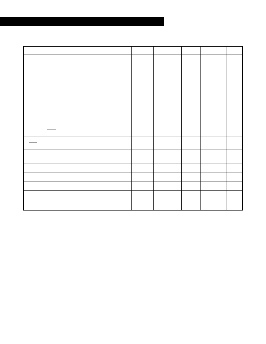
Pages 394 and 395, Table 23-4 5.0V DC Electrical Characteristics --
Delete LVI typical values and correct note 6.
From:
To:
3.3V DC Electrical
Characteristics
Pages 396 and 397, Table 23-5 3.3V DC Electrical Characteristics --
Delete LVI typical values and correct note 6.
From:
To:
Characteristic
Symbol
Min
Typ
Max
Unit
Low-voltage inhibit, trip falling voltage
V
TRIPF
4.00
4.32
4.70
V
Low-voltage inhibit, trip rising voltage
V
TRIPR
4.00
4.32
4.70
V
Notes:
6. LCD driver configured for high current mode.
Characteristic
Symbol
Min
Typ
Max
Unit
Low-voltage inhibit, trip falling voltage
V
TRIPF
4.00
--
4.70
V
Low-voltage inhibit, trip rising voltage
V
TRIPR
4.00
--
4.70
V
Notes:
6. LCD driver configured for low current mode.
Characteristic
Symbol
Min
Typ
Max
Unit
Low-voltage inhibit, trip falling voltage
V
TRIPF
2.40
2.57
2.88
V
Low-voltage inhibit, trip rising voltage
V
TRIPR
2.46
2.63
2.97
V
Notes:
6. LCD driver configured for high current mode.
Characteristic
Symbol
Min
Typ
Max
Unit
Low-voltage inhibit, trip falling voltage
V
TRIPF
2.40
--
2.88
V
Low-voltage inhibit, trip rising voltage
V
TRIPR
2.46
--
2.97
V
Notes:
6. LCD driver configured for low current mode.
F
r
e
e
s
c
a
l
e
S
e
m
i
c
o
n
d
u
c
t
o
r
,
I
Freescale Semiconductor, Inc.
For More Information On This Product,
Go to: www.freescale.com
n
c
.
.
.

HC908LJ12AD/D
14
Addendum to MC68HC908LJ12 Technical Data
MOTOROLA
Oscillator
Characteristics
Page 398, Table 23-8 5.0V Oscillator Specifications and Table 23-9 3.3V
Oscillator Specifications -- Replace Internal oscillator clock frequency
values.
From:
To:
See
Figure 1 . Typical Internal Oscillator Frequency
on page 6 of this
document.
-- END --
Characteristic
Symbol
Min
Typ
Max
Unit
Internal oscillator clock frequency
f
ICLK
46k
47k
48k
Hz
Characteristic
Symbol
Min
Typ
Max
Unit
Internal oscillator clock frequency
f
ICLK
42.8 k
43.4 k
44k
Hz
F
r
e
e
s
c
a
l
e
S
e
m
i
c
o
n
d
u
c
t
o
r
,
I
Freescale Semiconductor, Inc.
For More Information On This Product,
Go to: www.freescale.com
n
c
.
.
.

HC908LJ12AD/D
-- END --
MOTOROLA
Addendum to MC68HC908LJ12 Technical Data
15
F
r
e
e
s
c
a
l
e
S
e
m
i
c
o
n
d
u
c
t
o
r
,
I
Freescale Semiconductor, Inc.
For More Information On This Product,
Go to: www.freescale.com
n
c
.
.
.

Information in this document is provided solely to enable system and software
implementers to use Motorola products. There are no express or implied copyright
licenses granted hereunder to design or fabricate any integrated circuits or
integrated circuits based on the information in this document.
Motorola reserves the right to make changes without further notice to any products
herein. Motorola makes no warranty, representation or guarantee regarding the
suitability of its products for any particular purpose, nor does Motorola assume any
liability arising out of the application or use of any product or circuit, and specifically
disclaims any and all liability, including without limitation consequential or incidental
damages. "Typical" parameters which may be provided in Motorola data sheets
and/or specifications can and do vary in different applications and actual
performance may vary over time. All operating parameters, including "Typicals"
must be validated for each customer application by customer's technical experts.
Motorola does not convey any license under its patent rights nor the rights of
others. Motorola products are not designed, intended, or authorized for use as
components in systems intended for surgical implant into the body, or other
applications intended to support or sustain life, or for any other application in which
the failure of the Motorola product could create a situation where personal injury or
death may occur. Should Buyer purchase or use Motorola products for any such
unintended or unauthorized application, Buyer shall indemnify and hold Motorola
and its officers, employees, subsidiaries, affiliates, and distributors harmless
against all claims, costs, damages, and expenses, and reasonable attorney fees
arising out of, directly or indirectly, any claim of personal injury or death associated
with such unintended or unauthorized use, even if such claim alleges that Motorola
was negligent regarding the design or manufacture of the part.
Motorola and the Stylized M Logo are registered in the U.S. Patent and Trademark
Office. digital dna is a trademark of Motorola, Inc. All other product or service
names are the property of their respective owners. Motorola, Inc. is an Equal
Opportunity/Affirmative Action Employer.
© Motorola, Inc. 2003
HC908LJ12AD/D
Rev. 0
6/2003
HOW TO REACH US:
USA/EUROPE/LOCATIONS NOT LISTED:
Motorola Literature Distribution
P.O. Box 5405, Denver, Colorado 80217
1-800-521-6274 or 480-768-2130
JAPAN:
Motorola Japan Ltd.; SPS, Technical Information Center
3-20-1, Minami-Azabu Minato-ku, Tokyo 106-8573 Japan
81-3-3440-3569
ASIA/PACIFIC:
Motorola Semiconductors H.K. Ltd.
Silicon Harbour Centre, 2 Dai King Street
Tai Po Industrial Estate, Tai Po, N.T., Hong Kong
852-26668334
HOME PAGE:
http://motorola.com/semiconductors
F
r
e
e
s
c
a
l
e
S
e
m
i
c
o
n
d
u
c
t
o
r
,
I
Freescale Semiconductor, Inc.
For More Information On This Product,
Go to: www.freescale.com
n
c
.
.
.