 | –≠–ª–µ–∫—Ç—Ä–æ–Ω–Ω—ã–π –∫–æ–º–ø–æ–Ω–µ–Ω—Ç: 74LS196 | –°–∫–∞—á–∞—Ç—å:  PDF PDF  ZIP ZIP |
5-372
FAST AND LS TTL DATA
4-STAGE PRESETTABLE
RIPPLE COUNTERS
The SN54/74LS196 decade counter is partitioned into divide-by-two and di-
vide-by-five sections which can be combined to count either in BCD (8, 4, 2, 1)
sequence or in a bi-quinary mode producing a 50% duty cycle output. The
SN54/74LS197 contains divide-by-two and divide-by-eight sections which
can be combined to form a modulo-16 binary counter. Low Power Schottky
technology is used to achieve typical count rates of 70 MHz and power dis-
sipation of only 80 mW.
Both circuit types have a Master Reset (MR) input which overrides all other
inputs and asynchronously forces all outputs LOW. A Parallel Load input (PL)
overrides clocked operations and asynchronously loads the data on the Par-
allel Data inputs (Pn) into the flip-flops. This preset feature makes the circuits
usable as programmable counters. The circuits can also be used as 4-bit
latches, loading data from the Parallel Data inputs when PL is LOW and stor-
ing the data when PL is HIGH.
∑
Low Power Consumption -- Typically 80 mW
∑
High Counting Rates -- Typically 70 MHz
∑
Choice of Counting Modes -- BCD, Bi-Quinary, Binary
∑
Asynchronous Presettable
∑
Asynchronous Master Reset
∑
Easy Multistage Cascading
∑
Input Clamp Diodes Limit High Speed Termination Effects
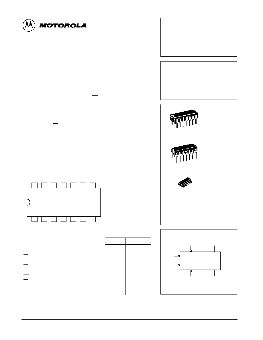
CONNECTION DIAGRAM DIP (TOP VIEW)
14
13
12
11
10
9
1
2
3
4
5
6
8
7
VCC MR
Q3
P3
P1
Q1 CP0
PL
Q2
P2
P0
Q0 CP1 GND
NOTE:
The Flatpak version
has the same pinouts
(Connection Diagram) as
the Dual In-Line Package.
PIN NAMES
LOADING (Note a)
HIGH
LOW
CP0
Clock (Active LOW Going Edge)
1.0 U.L.
1.5 U.L.
Input to Divide-by-Two Section
CP1 (LS196)
Clock (Active LOW Going Edge)
2.0 U.L.
1.75 U.L.
Input to Divide-by-Five Section
CP1 (LS197)
Clock (Active LOW Going Edge)
1.0 U.L.
0.8 U.L.
Input to Divide-by-Eight Section
MR
Master Reset (Active LOW) Input
1.0 U.L.
0.5 U.L.
PL
Parallel Load (Active LOW) Input
0.5 U.L.
0.25 U.L.
P0≠P3
Data Inputs
0.5 U.L.
0.25 U.L.
Q0≠Q3
Outputs (Notes b, c)
10 U.L.
5 (2.5) U.L.
NOTES:
a. 1 TTL Unit Load (U.L.) = 40
µ
A HIGH/1.6 mA LOW.
b. The Output LOW drive factor is 2.5 U.L. for Military (54) and 5 U.L. for Commercial (74)
b.
Temperature Ranges.
c. In addition to loading shown, Q0 can also drive CP1.
SN54/74LS196
SN54/74LS197
4-STAGE PRESETTABLE
RIPPLE COUNTERS
LOW POWER SCHOTTKY
J SUFFIX
CERAMIC
CASE 632-08
N SUFFIX
PLASTIC
CASE 646-06
14
1
14
1
ORDERING INFORMATION
SN54LSXXXJ
Ceramic
SN74LSXXXN
Plastic
SN74LSXXXD
SOIC
14
1
D SUFFIX
SOIC
CASE 751A-02
LOGIC SYMBOL
CP0
CP1
PL
MR
P0
Q0
P1 P2 P3
Q1 Q2Q3
1
4 10 3 11
12
2
9
5
13
6
8
VCC = PIN 14
GND = PIN 7
5-373
FAST AND LS TTL DATA
SN54/74LS196
∑
SN54/74LS197
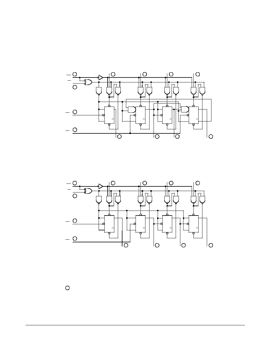
LOGIC DIAGRAM
LS196
LS197
MR
PL
CP0
CP1
P0
P1
P2
P3
Q0
Q1
Q2
Q3
J SD Q
KCD Q
1
2
6
3
8
4
5
9
11
12
10
13
J SD Q
KCD Q
J SD Q
KCD Q
J SD Q
KCD Q
VCC = PIN 14
GND = PIN 7
= PIN NUMBERS
MR
PL
CP0
CP1
P0
P1
P2
P3
Q0
Q1
Q2
Q3
J SD Q
KCD Q
1
2
6
3
8
4
5
9
11
12
10
13
J SD Q
KCD Q
J SD Q
KCD Q
J SD Q
KCD Q

5-374
FAST AND LS TTL DATA
SN54/74LS196
∑
SN54/74LS197
FUNCTIONAL DESCRIPTION
The LS196 and LS197 are asynchronously presettable de-
cade and binary ripple counters. The LS196 Decade Counter
is partitioned into divide-by-two and divide-by-five sections
while the LS197 is partitioned into divide-by-two and divide-
by-eight sections, with all sections having a separate Clock in-
put. In the counting modes, state changes are initiated by the
HIGH to LOW transition of the clock signals. State changes of
the Q outputs, however, do not occur simultaneously because
of the internal ripple delays. When using external logic to de-
code the Q outputs, designers should bear in mind that the un-
equal delays can lead to decoding spikes and thus a decoded
signal should not be used as a clock or strobe. The CP0 input
serves the Q0 flip-flop in both circuit types while the CP1 input
serves the divide-by-five or divide-by-eight section. The Q0
output is designed and specified to drive the rated fan-out plus
the CP1 input. With the input frequency connected to CP0 and
Q0 driving CP1, the LS197 forms a straightforward module-16
counter, with Q0 the least significant output and Q3 the most
significant output.
The LS196 Decade Counter can be connected up to oper-
ate in two different count sequences, as indicated in the tables
of Figure 2. With the input frequency connected to CP0 and
with Q0 driving CP1, the circuit counts in the BCD (8, 4, 2, 1)
sequence. With the input frequency connected to CP1 and Q3
driving CP0, Q0 becomes the low frequency output and has a
50% duty cycle waveform. Note that the maximum counting
rate is reduced in the latter (bi-quinary) configuration because
of the interstage gating delay within the divide-by-five section.
The LS196 and LS197 have an asynchronous active LOW
Master Reset input (MR) which overrides all other inputs and
forces all outputs LOW. The counters are also asynchronously
presettable. A LOW on the Parallel Load input (PL) overrides
the clock inputs and loads the data from Parallel Data (P0≠P3)
inputs into the flip-flops. While PL is LOW, the counters act as
transparent latches and any change in the Pn inputs will be re-
flected in the outputs.
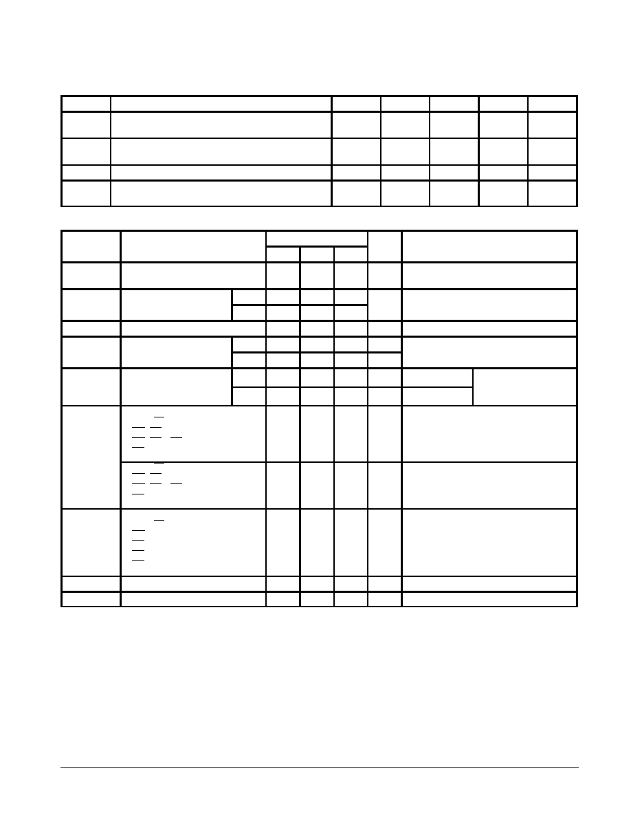
Figure 2. LS196 COUNT SEQUENCES
DECADE (NOTE 1)
BI-QUINARY (NOTE 2)
COUNT
Q3
Q2
Q1
Q0
COUNT
Q0
Q3
Q2
Q1
0
L
L
L
L
0
L
L
L
L
1
L
L
L
H
1
L
L
L
H
2
L
L
H
L
2
L
L
H
L
3
L
L
H
H
3
L
L
H
H
4
L
H
L
L
4
L
H
L
L
5
L
H
L
H
5
H
L
L
L
6
L
H
H
L
6
H
L
L
H
7
L
H
H
H
7
H
L
H
L
8
H
L
L
L
8
H
L
H
H
9
H
L
L
H
9
H
H
L
L
NOTES:
1. Signal applied to CP0, Q0 connected to CP1.
2. Signal applied to CP1, Q3 connected to CP0.
MODE SELECT TABLE
INPUTS
RESPONSE
MR
PL
CP
RESPONSE
L
X
X
Reset (Clear)
H
L
X
Parallel Load
H
H
Count
H = HIGH Voltage Level
L = LOW Voltage Level
X = Don't Care
= HIGH to Low Clock Transition
5-375
FAST AND LS TTL DATA
SN54/74LS196
∑
SN54/74LS197
GUARANTEED OPERATING RANGES
Symbol
Parameter
Min
Typ
Max
Unit
VCC
Supply Voltage
54
74
4.5
4.75
5.0
5.0
5.5
5.25
V
TA
Operating Ambient Temperature Range
54
74
≠ 55
0
25
25
125
70
∞
C
IOH
Output Current -- High
54, 74
≠ 0.4
mA
IOL
Output Current -- Low
54
74
4.0
8.0
mA
DC CHARACTERISTICS OVER OPERATING TEMPERATURE RANGE
(unless otherwise specified)
Symbol
Parameter
Limits
Unit
Test Conditions
Symbol
Parameter
Min
Typ
Max
Unit
Test Conditions
VIH
Input HIGH Voltage
2.0
V
Guaranteed Input HIGH Voltage for
All Inputs
VIL
Input LOW Voltage
54
0.7
V
Guaranteed Input LOW Voltage for
All Inputs
VIL
Input LOW Voltage
74
0.8
V
Guaranteed Input LOW Voltage for
All Inputs
VIK
Input Clamp Diode Voltage
≠ 0.65
≠ 1.5
V
VCC = MIN, IIN = ≠ 18 mA
VOH
Output HIGH Voltage
54
2.5
3.5
V
VCC = MIN, IOH = MAX, VIN = VIH
or VIL per Truth Table
VOH
Output HIGH Voltage
74
2.7
3.5
V
VCC = MIN, IOH = MAX, VIN = VIH
or VIL per Truth Table
VOL
Output LOW Voltage
54, 74
0.25
0.4
V
IOL = 4.0 mA
VCC = VCC MIN,
VIN = VIL or VIH
per Truth Table
VOL
Output LOW Voltage
74
0.35
0.5
V
IOL = 8.0 mA
VIN = VIL or VIH
per Truth Table
IIH
Input HIGH Current
Data, PL
MR, CP0 (LS196)
MR, CP0, CP1 (LS197)
CP1 (LS196)
20
40
40
80
µ
A
VCC = MAX, VIN = 2.7 V
IIH
Data, PL
MR, CP0 (LS196)
MR, CP0, CP1 (LS197)
CP1 (LS196)
0.1
0.2
0.2
0.4
mA
VCC = MAX, VIN = 7.0 V
IIL
Input LOW Current
Data, PL
MR
CP0
CP1 (LS196)
CP1 (LS197)
≠ 0.4
≠ 0.8
≠ 2.4
≠ 2.8
≠ 1.3
mA
VCC = MAX, VIN = 0.4 V
IOS
Short Circuit Current (Note 1)
≠ 20
≠ 100
mA
VCC = MAX
ICC
Power Supply Current
27
mA
VCC = MAX
Note 1: Not more than one output should be shorted at a time, nor for more than 1 second.

5-376
FAST AND LS TTL DATA
SN54/74LS196
∑
SN54/74LS197
AC CHARACTERISTICS
(TA = 25
∞
C)
Symbol
Parameter
Limits
Unit
Test Conditions
Symbol
Parameter
LS196
LS197
Unit
Test Conditions
Symbol
Parameter
Min
Typ
Max
Min
Typ
Max
Unit
Test Conditions
fMAX
Maximum Clock Frequency
30
40
30
40
MHz
VCC = 5.0 V
CL = 15 pF
tPLH
tPHL
CP0 Input to
Q0 Output
8.0
13
15
20
8.0
14
15
21
ns
VCC = 5.0 V
CL = 15 pF
tPLH
tPHL
CP1 Input to
Q1 Output
16
22
24
33
12
23
19
35
ns
VCC = 5.0 V
CL = 15 pF
tPLH
tPHL
CP1 Input to
Q2 Output
38
41
57
62
34
42
51
63
ns
VCC = 5.0 V
CL = 15 pF
tPLH
tPHL
CP1 Input to
Q3 Output
12
30
18
45
55
63
78
95
ns
VCC = 5.0 V
CL = 15 pF
tPLH
tPHL
Data to Output
20
29
30
44
18
29
27
44
ns
tPLH
tPHL
PL Input to
Any Output
27
30
41
45
26
30
39
45
ns
tPHL
MR Input to Any Output
34
51
34
51
ns
AC SETUP REQUIREMENTS
(TA = 25
∞
C)
Symbol
Parameter
Limits
Unit
Test Conditions
Symbol
Parameter
LS196
LS197
Unit
Test Conditions
Symbol
Parameter
Min
Typ
Max
Min
Typ
Max
Unit
Test Conditions
tW
CP0 Pulse Width
20
20
ns
VCC = 5.0 V
tW
CP1 Pulse Width
30
30
ns
VCC = 5.0 V
tW
PL Pulse Width
20
20
ns
VCC = 5.0 V
tW
MR Pulse Width
15
15
ns
VCC = 5.0 V
ts
Data Input Setup Time -- HIGH
10
10
ns
VCC = 5.0 V
ts
Data Input Setup Time -- LOW
15
15
ns
CC = 5.0 V
th
Data Hold Time -- HIGH
10
10
ns
th
Data Hold Time -- LOW
10
10
ns
trec
Recovery Time
30
30
ns
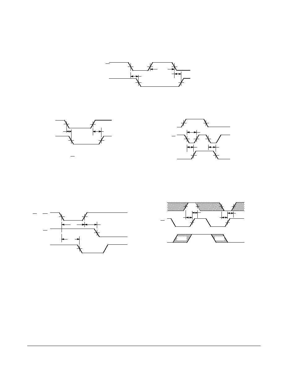
DEFINITIONS OF TERMS
SETUP TIME (ts) -- is defined as the minimum time required
for the correct logic level to be present at the logic input prior to
the clock transition from HIGH to LOW in order to be recog-
nized and transferred to the outputs.
HOLD TIME (th) -- is defined as the minimum time following
the clock transition from HIGH to LOW that the logic level must
be maintained at the input in order to ensure continued recog-
nition. A negative HOLD TIME indicates that the correct logic
level may be released prior to the clock transition from HIGH to
LOW and still be recognized.
RECOVERY TIME (trec) -- is defined as the minimum time
required between the end of the reset pulse and the clock
transition from HIGH to LOW in order to recognize and transfer
LOW Data to the Q outputs.
5-377
FAST AND LS TTL DATA
SN54/74LS196
∑
SN54/74LS197
AC WAVEFORMS
Pn
tW
tPHL
tPLH
1.3 V
1.3 V
PL
Qn
tW
tPHL
1.3 V
1.3 V
1.3 V
trec
PL OR MR
CP
Q
CP
1.3 V
1.3 V
1.3 V
1.3 V
tPHL
tPLH
tW(H)
Q
Figure 1
Figure 2
Figure 3
Figure 4
Figure 5
1.3 V
1.3 V
1.3 V
tPHL
tPLH
Pn
Qn
NOTE: PL = LOW
1.3 V
1.3 V
1.3 V
1.3 V
Pn*
PL
Qn*
ts(H)
ts(L)
th(H)
th(L)
* The shaded areas indicate when the input is permitted
*
to change for predictable output performance
Q = P
Q = P
5-378
FAST AND LS TTL DATA
MIN
MIN
MAX
MAX
MILLIMETERS
INCHES
DIM
A
B
C
D
F
G
J
K
M
P
R
8.55
3.80
1.35
0.35
0.40
0.19
0.10
0
∞
5.80
0.25
8.75
4.00
1.75
0.49
1.25
0.25
0.25
7
∞
6.20
0.50
0.337
0.150
0.054
0.014
0.016
0.008
0.004
0
∞
0.229
0.010
0.344
0.157
0.068
0.019
0.049
0.009
0.009
7
∞
0.244
0.019
1.27 BSC
0.050 BSC
NOTES:
1. DIMENSIONS A" AND B" ARE DATUMS AND
T" IS A DATUM SURFACE.
2. DIMENSIONING AND TOLERANCING PER ANSI
Y14.5M, 1982.
3. CONTROLLING DIMENSION: MILLIMETER.
4. DIMENSION A AND B DO NOT INCLUDE MOLD
PROTRUSION.
5. MAXIMUM MOLD PROTRUSION 0.15 (0.006)
PER SIDE.
6. 751A 01 IS OBSOLETE, NEW STANDARD
751A 02.
-A-
-B-
P
G
C
K
SEATING
PLANE
14 PL
D
M
F
J
7 PL
R X 45
∞
1
7
8
14
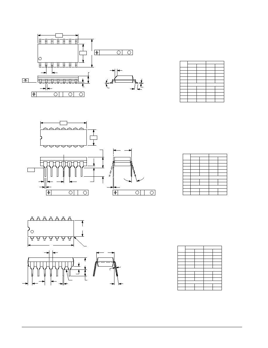
Case 751A-02 D Suffix
14-Pin Plastic
SO-14
B
0.25 (0.010)
M
M
T
0.25 (0.010)
B
A
M
S
S
Case 632-08 J Suffix
14-Pin Ceramic Dual In-Line
MIN
MIN
MAX
MAX
MILLIMETERS
INCHES
DIM
A
B
C
D
F
G
J
K
L
M
N
19.05
6.23
3.94
0.39
1.40
0.21
3.18
0
∞
0.51
19.94
7.11
5.08
0.50
1.65
0.38
4.31
15
∞
1.01
0.750
0.245
0.155
0.015
0.055
0.008
0.125
0
∞
0.020
0.785
0.280
0.200
0.020
0.065
0.015
0.170
15
∞
0.040
2.54 BSC
7.62 BSC
0.100 BSC
0.300 BSC
NOTES:
1. DIMENSIONING AND TOLERANCING PER ANSI
Y14.5M, 1982.
2. CONTROLLING DIMENSION: INCH.
3. DIMENSION L TO CENTER OF LEAD WHEN
FORMED PARALLEL.
4. DIM F MAY NARROW TO 0.76 (0.030) WHERE
THE LEAD ENTERS THE CERAMIC BODY.
5. 632 01 THRU 07 OBSOLETE, NEW STANDARD
632 08.
14
8
1
7
-A-
-B-
-T-
SEATING
PLANE
F
G
D
14 PL
N
K
C
L
J
14 PL
M
0.25 (0.010)
T A
M
S
0.25 (0.010)
T B
M
S
Case 646-06 N Suffix
14-Pin Plastic
MIN
MIN
MAX
MAX
MILLIMETERS
INCHES
DIM
18.16
6.10
3.69
0.38
1.02
1.32
0.20
2.92
19.56
6.60
4.69
0.53
1.78
2.41
0.38
3.43
0
∞
0.39
0.715
0.240
0.145
0.015
0.040
0.052
0.008
0.115
0.770
0.260
0.185
0.021
0.070
0.095
0.015
0.135
10
∞
1.01
2.54 BSC
7.62 BSC
0.100 BSC
0.300 BSC
0
∞
0.015
10
∞
0.039
A
B
C
D
F
G
H
J
K
L
M
N
NOTES:
1. LEADS WITHIN 0.13 mm (0.005) RADIUS OF TRUE
POSITION AT SEATING PLANE AT MAXIMUM
MATERIAL CONDITION.
2. DIMENSION L" TO CENTER OF LEADS WHEN
FORMED PARALLEL.
3. DIMENSION B" DOES NOT INCLUDE MOLD
FLASH.
4. ROUNDED CORNERS OPTIONAL.
5. 646 05 OBSOLETE, NEW STANDARD 646 06.
1
7
14
8
B
A
NOTE 4
F
H
G
D
SEATING
PLANE
N
K
C
L
J
M

5-379
FAST AND LS TTL DATA
Motorola reserves the right to make changes without further notice to any products herein. Motorola makes no warranty, representation or guarantee regarding
the suitability of its products for any particular purpose, nor does Motorola assume any liability arising out of the application or use of any product or circuit,
and specifically disclaims any and all liability, including without limitation consequential or incidental damages. "Typical" parameters can and do vary in different
applications. All operating parameters, including "Typicals" must be validated for each customer application by customer's technical experts. Motorola does
not convey any license under its patent rights nor the rights of others. Motorola products are not designed, intended, or authorized for use as components in
systems intended for surgical implant into the body, or other applications intended to support or sustain life, or for any other application in which the failure of
the Motorola product could create a situation where personal injury or death may occur. Should Buyer purchase or use Motorola products for any such
unintended or unauthorized application, Buyer shall indemnify and hold Motorola and its officers, employees, subsidiaries, affiliates, and distributors harmless
against all claims, costs, damages, and expenses, and reasonable attorney fees arising out of, directly or indirectly, any claim of personal injury or death
associated with such unintended or unauthorized use, even if such claim alleges that Motorola was negligent regarding the design or manufacture of the part.
Motorola and
are registered trademarks of Motorola, Inc. Motorola, Inc. is an Equal Opportunity/Affirmative Action Employer.
Literature Distribution Centers:
USA: Motorola Literature Distribution; P.O. Box 20912; Phoenix, Arizona 85036.
EUROPE: Motorola Ltd.; European Literature Centre; 88 Tanners Drive, Blakelands, Milton Keynes, MK14 5BP, England.
JAPAN: Nippon Motorola Ltd.; 4-32-1, Nishi-Gotanda, Shinagawa-ku, Tokyo 141, Japan.
ASIA PACIFIC: Motorola Semiconductors H.K. Ltd.; Silicon Harbour Center, No. 2 Dai King Street, Tai Po Industrial Estate, Tai Po, N.T., Hong Kong.