 | –≠–ª–µ–∫—Ç—Ä–æ–Ω–Ω—ã–π –∫–æ–º–ø–æ–Ω–µ–Ω—Ç: 74LS348 | –°–∫–∞—á–∞—Ç—å:  PDF PDF  ZIP ZIP |
5-499
FAST AND LS TTL DATA
8-INPUT PRIORITY ENCODERS
WITH 3-STATE OUTPUTS
The SN54 / 74LS348 and the SN54 / 74LS848 are eight input priority encod-
ers which provide the 8-line to 3-line function.
The outputs (A0 ≠ A2) and inputs (0 ≠ 7) are active low. The active low input
which has the highest priority (input 7 has the highest) is represented on the
outputs (output A0 is the lowest bit). An example would be if inputs 1, 2 and 4
were low, then a binary 4 would be represented on the outputs.
The GS (Group Signal) output is active low when any of the inputs are low. It
serves to indicate when any of the inputs are active.
A0, A1 and A2 are three-state outputs. This allows for up to 64 line expan-
sion without the need for special external circuitry.
A logical one on the Enable Input (EI) forces A0, A1 ared A2 to the disabled
state and outputs GS and EO to the high state. A high on all data inputs (0 ≠ 7)
together with a low on the EI input disables outputs A0, A1, and A2 and forces
output GS to the high state and output EO to the low state.
Use of the EI input in conjunction with the EO output provides for the capa-
bility of having priority encoding of n input signals.
The LS848 has special internal circuitry providing for a greatly reduced neg-
ative going glitch on the GS (Group Signal) output and on a reduced tendency
for the A0, A1 and A2 outputs to become momentarily enabled. Both of these
occurrences happen when the EI input goes from a logical one to a logical zero
and all data inputs (0 ≠ 7) are held at logical ones. The internal glitch reduction
circuitry does add an additional fan-in of one on all data inputs (compared to
that of the LS348).
14
13
12
11
10
9
1
2
3
4
5
6
7
16
15
8
VCC
4
EO
GS
3
2
0
1
OUTPUT
A0
5
6
7
EI
A2
A1 GND
OUTPUTS
INPUTS
OUTPUTS
INPUTS
EO
GS
3
2
0
1
5
6
7
EI
A2
A1
4
A0
FUNCTION TABLE
INPUTS
OUTPUTS
EI
0
1
2
3
4
5
6
7
A2
A1
A0
GS
EO
H
X X X
X X X
X X
Z
Z
Z
H
H
L
H H H H H H H H
Z
Z
Z
H
L
L
X X X
X X X
X
L
L
L
L
L
H
L
X X X
X X X
L
H
L
L
H
L
H
L
X X X
X X
L
H H
L
H
L
L
H
L
X X X
X
L
H H H
L
H
H
L
H
L
X X X
L
H H H H
H
L
L
L
H
L
X X
L
H H H H H
H
L
H
L
H
L
X
L
H H H H H H
H
H
L
L
H
L
L
H H H H H H H
H
H
H
L
H
SN54/74LS348
SN54/74LS848
8-INPUT PRIORITY ENCODERS
WITH 3-STATE OUTPUTS
LOW POWER SCHOTTKY
ORDERING INFORMATION
SN54LSXXXJ
Ceramic
SN74LSXXXN
Plastic
SN74LSXXXD
SOIC
J SUFFIX
CERAMIC
CASE 620-09
N SUFFIX
PLASTIC
CASE 648-08
16
1
16
1
16
1
D SUFFIX
SOIC
CASE 751B-03
H = HIGH Logic Level
L = LOW Logic Level
X = Irrelevant
Z = High Impedance State
5-500
FAST AND LS TTL DATA
SN54/74LS348
∑
SN54/74LS848
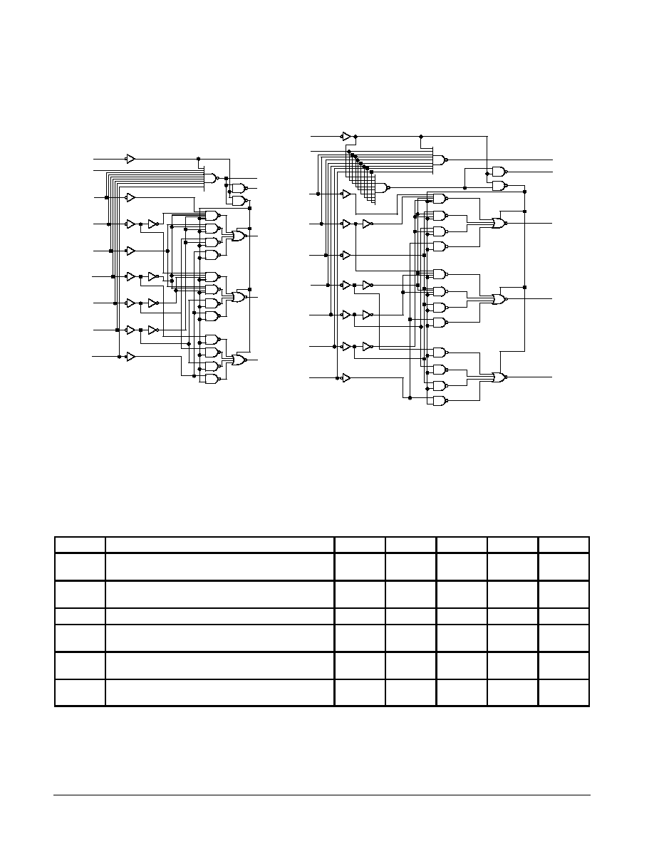
BLOCK DIAGRAMS
SN54 / 74LS348
SN54 / 74LS848
EI
0
1
2
3
4
5
6
7
(5)
(10)
(11)
(12)
(13)
(1)
(2)
(3)
(4)
EO
GS
A0
A1
A2
(15)
(14)
(9)
(7)
(6)
EI
0
1
2
3
4
5
6
7
(5)
(10)
(11)
(12)
(13)
(1)
(2)
(3)
(4)
EO
GS
A0
A1
A2
(15)
(14)
(9)
(7)
(6)
G1
G2
G3
G4
G5
G6
G7
G8
G9
G10
G11
G12
G31
G13
G14
G15
G16
G17
G18
G19
G20
G21
G22
G24
G25
G26
G27
G29
G30
G23
G28
GUARANTEED OPERATING RANGES
Symbol
Parameter
Min
Typ
Max
Unit
VCC
Supply Voltage
54
74
4.5
4.75
5.0
5.0
5.5
5.25
V
TA
Operating Ambient Temperature Range
54
74
≠ 55
0
25
25
125
70
∞
C
IOH
Output Current -- High
EO, GS
54, 74
≠ 0.4
mA
IOH
Output Current -- High
A0, A1, A2
A0, A1, A2
54
74
≠ 1.0
≠ 2.6
mA
IOL
Output Current -- Low
EO, GS
54
74
4.0
8.0
mA
IOL
Output Current -- Low
A0, A1, A2
A0, A1, A2
54
74
12
24
mA

5-501
FAST AND LS TTL DATA
SN54/74LS348
∑
SN54/74LS848
DC CHARACTERISTICS OVER OPERATING TEMPERATURE RANGE
(unless otherwise specified)
Symbol
Parameter
Limits
Unit
Test Conditions
Symbol
Parameter
Min
Typ
Max
Unit
Test Conditions
VIH
Input HIGH Voltage
2.0
V
Guaranteed Input HIGH Voltage for
All Inputs
VIL
Input LOW Voltage
54
0.7
V
Guaranteed Input LOW Voltage for
All Inputs
VIL
Input LOW Voltage
74
0.8
V
Guaranteed Input LOW Voltage for
All Inputs
VIK
Input Clamp Diode Voltage
≠ 0.65
≠ 1.5
V
VCC = MIN, IIN = ≠ 18 mA
VOH
Output HIGH Voltage
A0, A1, A2
54, 74
2.4
3.1
V
VCC = MIN, IOH = MAX, VIN = VIH
or VIL per Truth Table
VOH
EO, GS
54
2.5
3.5
V
VCC = MIN, IOH = MAX, VIN = VIH
or VIL per Truth Table
EO, GS
74
2.7
3.5
V
VOL
Output LOW Voltage
EO, GS
54, 74
0.25
0.4
V
IOL = 4.0 mA
VCC = VCC MIN,
VIN = VIL or VIH
per Truth Table
VOL
Output LOW Voltage
EO, GS
74
0.35
0.5
V
IOL = 8.0 mA
VIN = VIL or VIH
per Truth Table
VOL
Output LOW Voltage
A0, A1, A2
54, 74
0.25
0.4
V
IOL = 12 mA
VCC = VCC MIN,
VIN = VIL or VIH
per Truth Table
VOL
Output LOW Voltage
A0, A1, A2
74
0.35
0.5
V
IOL = 24 mA
VIN = VIL or VIH
per Truth Table
IOZH
Output Off Current HIGH
20
µ
A
VCC = MAX, VOUT = 2.7 V
IOZL
Output Off Current LOW
≠20
µ
A
VCC = MAX, VOUT = 0.4 V
IIH
Input HIGH Current
Input 0, EI -- LS348
20
µ
A
VCC = MAX, VIN = 2.7 V
IIH
Input 0 -- LS848
40
µ
A
VCC = MAX, VIN = 2.7 V
IIH
Other -- LS348
Other -- LS848
40
60
µ
A
µ
A
CC = MAX, VIN = 2.7 V
IIH
Input HIGH Current
Input 0, EI -- LS348
0.1
mA
VCC = MAX, VIN = 7.0 V
Input 0 -- LS848
0.2
mA
VCC = MAX, VIN = 7.0 V
Other -- LS348
Other -- LS848
0.2
0.3
mA
mA
CC = MAX, VIN = 7.0 V
IIL
Input LOW Current
Input 0, EI -- LS348
≠ 0.4
mA
VCC = MAX, VIN = 0.4 V
IIL
Input 0 -- LS848
≠ 0.8
mA
VCC = MAX, VIN = 0.4 V
IL
Other -- LS348
Other -- LS848
≠ 0.8
≠ 1.2
mA
mA
CC = MAX, VIN = 0.4 V
IOS
Short Circuit Current (Note 1)
EO, GS
≠ 20
≠ 120
mA
VCC = MAX
IOS
EO, GS
A0, A1, A2
≠ 30
≠ 130
mA
VCC = MAX
ICC
Power Supply Current
Total, Output HIGH
12
23
mA
VCC = MAX
All Inputs and Outputs Open
ICC
Total, Output LOW
13
25
mA
VCC = MAX, Inputs 7, EI = GND
All Others Open
Note 1: Not more than one output should be shorted at a time, nor for more than 1 second.

5-502
FAST AND LS TTL DATA
SN54/74LS348
∑
SN54/74LS848
AC CHARACTERISTICS
(VCC = 5.0 V, TA = 25
∞
C)
Symbol
From
(Input)
To
(Output)
Waveform
LS348
Limits
LS848
Limits
Unit
Test Conditions
Symbol
From
(Input)
To
(Output)
Waveform
Min
Typ
Max
Min
Typ
Max
Unit
Test Conditions
tPLH
1 thru 7
A0, A1 or A2
In-Phase
11
17
12
18
ns
CL = 45 pF
RL = 667
tPHL
1 thru 7
A0, A1 or A2
output
20
30
20
30
ns
CL = 45 pF
RL = 667
tPLH
1 thru 7
A0, A1 or A2
Out-of-Phase
23
35
23
35
ns
CL = 45 pF
RL = 667
tPHL
1 thru 7
A0, A1 or A2
output
23
35
23
35
ns
CL = 45 pF
RL = 667
tPZH
EI
A0, A1 or A2
25
39
25
39
ns
tPZL
EI
A0, A1 or A2
24
41
24
41
ns
tPLH
0 thru 7
E0
Out-of-Phase
11
18
11
18
ns
CL = 15 pF
RL = 2.0
tPHL
0 thru 7
E0
output
26
40
26
40
ns
CL = 15 pF
RL = 2.0
tPLH
0 thru 7
GS
In-Phase
38
55
38
55
ns
CL = 15 pF
RL = 2.0
tPHL
0 thru 7
GS
output
9.0
21
9.0
21
ns
CL = 15 pF
RL = 2.0
tPLH
EI
GS
In-Phase
11
17
11
17
ns
CL = 15 pF
RL = 2.0
tPHL
EI
GS
output
14
36
14
36
ns
tPLH
EI
EO
In-Phase
17
21
17
21
ns
tPHL
EI
EO
output
25
40
30
45
ns
tPHZ
EI
A0, A1 or A2
18
27
18
27
ns
CL = 5.0 pF
RL = 667
tPLZ
EI
A0, A1 or A2
23
35
23
35
ns
CL = 5.0 pF
RL = 667

5-503
FAST AND LS TTL DATA
MIN
MIN
MAX
MAX
MILLIMETERS
INCHES
DIM
A
B
C
D
F
G
J
K
M
P
R
9.80
3.80
1.35
0.35
0.40
0.19
0.10
0
∞
5.80
0.25
10.00
4.00
1.75
0.49
1.25
0.25
0.25
7
∞
6.20
0.50
0.386
0.150
0.054
0.014
0.016
0.008
0.004
0
∞
0.229
0.010
0.393
0.157
0.068
0.019
0.049
0.009
0.009
7
∞
0.244
0.019
1.27 BSC
0.050 BSC
NOTES:
1. DIMENSIONING AND TOLERANCING PER ANSI
Y14.5M, 1982.
2. CONTROLLING DIMENSION: MILLIMETER.
3. DIMENSION A AND B DO NOT INCLUDE MOLD
PROTRUSION.
4. MAXIMUM MOLD PROTRUSION 0.15 (0.006)
PER SIDE.
5. 751B 01 IS OBSOLETE, NEW STANDARD
751B 03.
1
8
9
16
-A-
-B-
P
16 PL
D
-T-
K
C
G
M
R X 45
∞
F
J
8 PL
SEATING
PLANE
Case 751B-03 D Suffix
16-Pin Plastic
SO-16
B
0.25 (0.010)
M
M
T
0.25 (0.010)
B
A
M
S
S
Case 648-08 N Suffix
16-Pin Plastic
MIN
MIN
MAX
MAX
MILLIMETERS
INCHES
DIM
A
B
C
D
F
G
H
J
K
L
M
S
18.80
6.35
3.69
0.39
1.02
0.21
2.80
7.50
0
∞
0.51
19.55
6.85
4.44
0.53
1.77
0.38
3.30
7.74
10
∞
1.01
0.740
0.250
0.145
0.015
0.040
0.008
0.110
0.295
0
∞
0.020
0.770
0.270
0.175
0.021
0.070
0.015
0.130
0.305
10
∞
0.040
NOTES:
1. DIMENSIONING AND TOLERANCING PER ANSI
Y14.5M, 1982.
2. CONTROLLING DIMENSION: INCH.
3. DIMENSION L" TO CENTER OF LEADS WHEN
FORMED PARALLEL.
4. DIMENSION B" DOES NOT INCLUDE MOLD
FLASH.
5. ROUNDED CORNERS OPTIONAL.
6. 648 01 THRU 07 OBSOLETE, NEW STANDARD
648 08.
2.54 BSC
1.27 BSC
0.100 BSC
0.050 BSC
-A-
B
1
8
9
16
F
H
G
D
16 PL
S
C
-T-
SEATING
PLANE
K
J
M
L
T A
0.25 (0.010)
M
M
Case 620-09 J Suffix
16-Pin Ceramic Dual In-Line
MIN
MIN
MAX
MAX
MILLIMETERS
INCHES
DIM
19.05
6.10
0.39
1.40
0.23
0
∞
0.39
19.55
7.36
4.19
0.53
1.77
0.27
5.08
15
∞
0.88
0.750
0.240
0.015
0.055
0.009
0
∞
0.015
0.770
0.290
0.165
0.021
0.070
0.011
0.200
15
∞
0.035
1.27 BSC
2.54 BSC
7.62 BSC
0.050 BSC
0.100 BSC
0.300 BSC
A
B
C
D
E
F
G
J
K
L
M
N
NOTES:
1. DIMENSIONING AND TOLERANCING PER ANSI
Y14.5M, 1982.
2. CONTROLLING DIMENSION: INCH.
3. DIMENSION L TO CENTER OF LEAD WHEN
FORMED PARALLEL.
4. DIM F MAY NARROW TO 0.76 (0.030) WHERE
THE LEAD ENTERS THE CERAMIC BODY.
5. 620 01 THRU 08 OBSOLETE, NEW STANDARD
620 09.
-B-
-A-
16 PL
-T-
C
D
E
F
G
J
K
M
N
SEATING
PLANE
16 PL
L
16
9
1
8
0.25 (0.010)
T A
M
S
0.25 (0.010)
T B
M
S

5-504
FAST AND LS TTL DATA
Motorola reserves the right to make changes without further notice to any products herein. Motorola makes no warranty, representation or guarantee regarding
the suitability of its products for any particular purpose, nor does Motorola assume any liability arising out of the application or use of any product or circuit,
and specifically disclaims any and all liability, including without limitation consequential or incidental damages. "Typical" parameters can and do vary in different
applications. All operating parameters, including "Typicals" must be validated for each customer application by customer's technical experts. Motorola does
not convey any license under its patent rights nor the rights of others. Motorola products are not designed, intended, or authorized for use as components in
systems intended for surgical implant into the body, or other applications intended to support or sustain life, or for any other application in which the failure of
the Motorola product could create a situation where personal injury or death may occur. Should Buyer purchase or use Motorola products for any such
unintended or unauthorized application, Buyer shall indemnify and hold Motorola and its officers, employees, subsidiaries, affiliates, and distributors harmless
against all claims, costs, damages, and expenses, and reasonable attorney fees arising out of, directly or indirectly, any claim of personal injury or death
associated with such unintended or unauthorized use, even if such claim alleges that Motorola was negligent regarding the design or manufacture of the part.
Motorola and
are registered trademarks of Motorola, Inc. Motorola, Inc. is an Equal Opportunity/Affirmative Action Employer.
Literature Distribution Centers:
USA: Motorola Literature Distribution; P.O. Box 20912; Phoenix, Arizona 85036.
EUROPE: Motorola Ltd.; European Literature Centre; 88 Tanners Drive, Blakelands, Milton Keynes, MK14 5BP, England.
JAPAN: Nippon Motorola Ltd.; 4-32-1, Nishi-Gotanda, Shinagawa-ku, Tokyo 141, Japan.
ASIA PACIFIC: Motorola Semiconductors H.K. Ltd.; Silicon Harbour Center, No. 2 Dai King Street, Tai Po Industrial Estate, Tai Po, N.T., Hong Kong.