 | ÐлекÑÑоннÑй компоненÑ: HC646 | СкаÑаÑÑ:  PDF PDF  ZIP ZIP |
Äîêóìåíòàöèÿ è îïèñàíèÿ www.docs.chipfind.ru
MOTOROLA
SEMICONDUCTOR TECHNICAL DATA
31
REV 6
©
Motorola, Inc. 1995
10/95
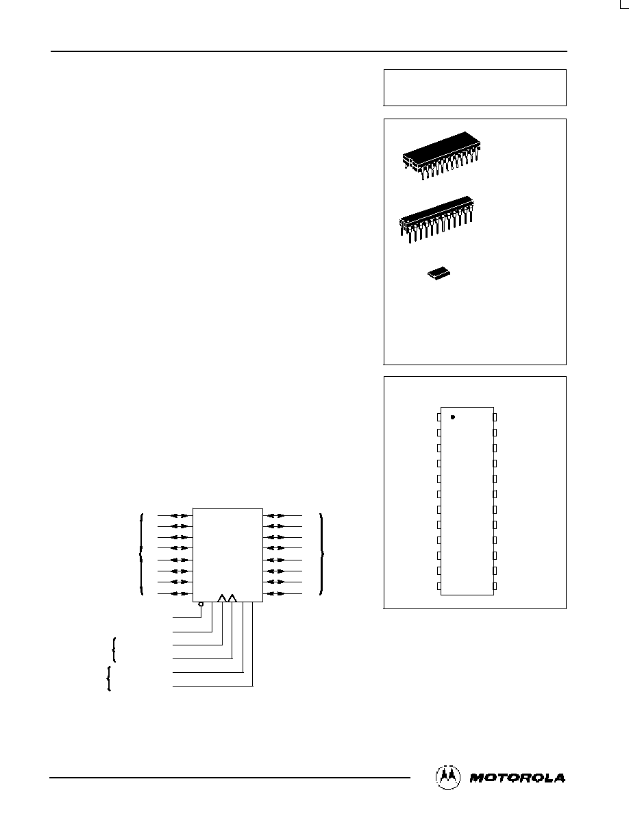
Octal 3-State Bus Transceivers
and D Flip-Flops
HighPerformance SiliconGate CMOS
The MC54/74HC646 is identical in pinout to the LS646. The device inputs
are compatible with standard CMOS outputs; with pullup resistors, they are
compatible with LSTTL outputs.
These devices are bus transceivers with D flipflops. Depending on the
status of the DataSource Selection pins, data may be routed to the outputs
either from the flipflops or transmitted realtime from the inputs (see
Function Table and Application Information).
The Output Enable and the Direction pins control the transceiver's
function. Bus A and Bus B cannot be routed as outputs to each other
simultaneously, but can be routed as inputs to the A and B flipflops. Also,
the A and B flipflops can be routed as outputs to Bus A and Bus B.
Additionally, when either or both of the ports are in the highimpedance
state, these I/O pins may be used as inputs to the D flipflops for data
storage.
The user should note that because the clocks are not gated with the
Direction and Output Enable pins, data at the A and B ports may be clocked
into the storage flipflops at any time.
·
Output Drive Capability: 15 LSTTL Loads
·
Outputs Directly Interface to CMOS, NMOS, and TTL
·
Operating Voltage Range: 2 to 6 V
·
Low Input Current: 1
µ
A
·
High Noise Immunity Characteristic of CMOS Devices
·
In Compliance with the Requirements Defined by JEDEC Standard
No. 7A
·
Chip Complexity: 780 FETs or 195 Equivalent Gates
LOGIC DIAGRAM
A
DATA
PORT
B
DATA
PORT
A0
A1
A2
A3
A4
A5
A6
A7
11
10
9
8
7
6
5
4
20
B0
19
18
17
16
15
14
13
B1
B2
B3
B4
B5
B6
B7
21
3
1
23
2
22
ATOB SOURCE
BTOA SOURCE
BTOA CLOCK
ATOB CLOCK
DIRECTION
OUTPUT ENABLE
FLIPFLOP
CLOCKS
DATA SOURCE
SELECTION
INPUTS
PIN 24 = VCC
PIN 12 = GND
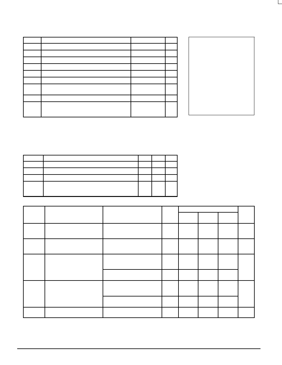
MC54/74HC646
PIN ASSIGNMENT
A2
A0
DIRECTION
ATOB
SOURCE
ATOB
CLOCK
A4
A3
A1
B0
OUTPUT ENABLE
BTOA
SOURCE
BTOA
CLOCK
VCC
B5
B4
B3
5
4
3
2
1
10
9
8
7
6
14
15
16
17
18
19
20
13
11
12
21
22
23
24
B7
B6
B2
B1
A7
GND
A6
A5
N SUFFIX
PLASTIC PACKAGE
CASE 72403
ORDERING INFORMATION
MC54HCXXXJ
MC74HCXXXN
MC74HCXXXDW
Ceramic
Plastic
SOIC
1
24
J SUFFIX
CERAMIC PACKAGE
CASE 75802
DW SUFFIX
SOIC PACKAGE
CASE 751E04
1
24
1
24
MC54/74HC646
MOTOROLA
HighSpeed CMOS Logic Data
DL129 -- Rev 6
32
ÎÎÎÎÎÎÎÎÎÎÎÎÎÎÎÎÎÎÎÎÎÎÎ
ÎÎÎÎÎÎÎÎÎÎÎÎÎÎÎÎÎÎÎÎÎÎÎ
ÎÎÎÎÎÎÎÎÎÎÎÎÎÎÎÎÎÎÎÎÎÎÎ
ÎÎÎÎÎÎÎÎÎÎÎÎÎÎÎÎÎÎÎÎÎÎÎ
MAXIMUM RATINGS*
ÎÎÎ
ÎÎÎ
ÎÎÎ
ÎÎÎ
Symbol
ÎÎÎÎÎÎÎÎÎÎÎÎÎÎ
ÎÎÎÎÎÎÎÎÎÎÎÎÎÎ
ÎÎÎÎÎÎÎÎÎÎÎÎÎÎ
ÎÎÎÎÎÎÎÎÎÎÎÎÎÎ
Parameter
ÎÎÎÎÎÎ
ÎÎÎÎÎÎ
ÎÎÎÎÎÎ
ÎÎÎÎÎÎ
Value
ÎÎÎ
ÎÎÎ
ÎÎÎ
ÎÎÎ
Unit
ÎÎÎ
ÎÎÎ
ÎÎÎ
ÎÎÎ
VCC
ÎÎÎÎÎÎÎÎÎÎÎÎÎÎ
ÎÎÎÎÎÎÎÎÎÎÎÎÎÎ
ÎÎÎÎÎÎÎÎÎÎÎÎÎÎ
ÎÎÎÎÎÎÎÎÎÎÎÎÎÎ
DC Supply Voltage (Referenced to GND)
ÎÎÎÎÎÎ
ÎÎÎÎÎÎ
ÎÎÎÎÎÎ
ÎÎÎÎÎÎ
0.5 to + 7.0
ÎÎÎ
ÎÎÎ
ÎÎÎ
ÎÎÎ
V
ÎÎÎ
ÎÎÎ
ÎÎÎ
ÎÎÎ
Vin
ÎÎÎÎÎÎÎÎÎÎÎÎÎÎ
ÎÎÎÎÎÎÎÎÎÎÎÎÎÎ
ÎÎÎÎÎÎÎÎÎÎÎÎÎÎ
ÎÎÎÎÎÎÎÎÎÎÎÎÎÎ
DC Input Voltage (Referenced to GND)
ÎÎÎÎÎÎ
ÎÎÎÎÎÎ
ÎÎÎÎÎÎ
ÎÎÎÎÎÎ
1.5 to VCC + 1.5
ÎÎÎ
ÎÎÎ
ÎÎÎ
ÎÎÎ
V
ÎÎÎ
ÎÎÎ
ÎÎÎ
ÎÎÎ
VI/O
ÎÎÎÎÎÎÎÎÎÎÎÎÎÎ
ÎÎÎÎÎÎÎÎÎÎÎÎÎÎ
ÎÎÎÎÎÎÎÎÎÎÎÎÎÎ
ÎÎÎÎÎÎÎÎÎÎÎÎÎÎ
DC I/O Voltage (Referenced to GND)
ÎÎÎÎÎÎ
ÎÎÎÎÎÎ
ÎÎÎÎÎÎ
ÎÎÎÎÎÎ
0.5 to VCC + 0.5
ÎÎÎ
ÎÎÎ
ÎÎÎ
ÎÎÎ
V
ÎÎÎ
ÎÎÎ
ÎÎÎ
ÎÎÎ
Iin
ÎÎÎÎÎÎÎÎÎÎÎÎÎÎ
ÎÎÎÎÎÎÎÎÎÎÎÎÎÎ
ÎÎÎÎÎÎÎÎÎÎÎÎÎÎ
ÎÎÎÎÎÎÎÎÎÎÎÎÎÎ
DC Input Current, per Pin
ÎÎÎÎÎÎ
ÎÎÎÎÎÎ
ÎÎÎÎÎÎ
ÎÎÎÎÎÎ
±
20
ÎÎÎ
ÎÎÎ
ÎÎÎ
ÎÎÎ
mA
ÎÎÎ
ÎÎÎ
ÎÎÎ
ÎÎÎ
II/O
ÎÎÎÎÎÎÎÎÎÎÎÎÎÎ
ÎÎÎÎÎÎÎÎÎÎÎÎÎÎ
ÎÎÎÎÎÎÎÎÎÎÎÎÎÎ
ÎÎÎÎÎÎÎÎÎÎÎÎÎÎ
DC I/O Current, per Pin
ÎÎÎÎÎÎ
ÎÎÎÎÎÎ
ÎÎÎÎÎÎ
ÎÎÎÎÎÎ
±
35
ÎÎÎ
ÎÎÎ
ÎÎÎ
ÎÎÎ
mA
ÎÎÎ
ÎÎÎ
ÎÎÎ
ÎÎÎ
ICC
ÎÎÎÎÎÎÎÎÎÎÎÎÎÎ
ÎÎÎÎÎÎÎÎÎÎÎÎÎÎ
ÎÎÎÎÎÎÎÎÎÎÎÎÎÎ
ÎÎÎÎÎÎÎÎÎÎÎÎÎÎ
DC Supply Current, VCC and GND Pins
ÎÎÎÎÎÎ
ÎÎÎÎÎÎ
ÎÎÎÎÎÎ
ÎÎÎÎÎÎ
±
75
ÎÎÎ
ÎÎÎ
ÎÎÎ
ÎÎÎ
mA
ÎÎÎ
ÎÎÎ
ÎÎÎ
ÎÎÎ
PD
ÎÎÎÎÎÎÎÎÎÎÎÎÎÎ
ÎÎÎÎÎÎÎÎÎÎÎÎÎÎ
ÎÎÎÎÎÎÎÎÎÎÎÎÎÎ
ÎÎÎÎÎÎÎÎÎÎÎÎÎÎ
Power Dissipation in Still Air, Plastic or Ceramic DIP
SOIC Package
ÎÎÎÎÎÎ
ÎÎÎÎÎÎ
ÎÎÎÎÎÎ
ÎÎÎÎÎÎ
750
500
ÎÎÎ
ÎÎÎ
ÎÎÎ
ÎÎÎ
mW
ÎÎÎ
ÎÎÎ
ÎÎÎ
ÎÎÎ
Tstg
ÎÎÎÎÎÎÎÎÎÎÎÎÎÎ
ÎÎÎÎÎÎÎÎÎÎÎÎÎÎ
ÎÎÎÎÎÎÎÎÎÎÎÎÎÎ
ÎÎÎÎÎÎÎÎÎÎÎÎÎÎ
Storage Temperature
ÎÎÎÎÎÎ
ÎÎÎÎÎÎ
ÎÎÎÎÎÎ
ÎÎÎÎÎÎ
65 to + 150
ÎÎÎ
ÎÎÎ
ÎÎÎ
ÎÎÎ
_
C
ÎÎÎ
ÎÎÎ
ÎÎÎ
ÎÎÎ
ÎÎÎ
TL
ÎÎÎÎÎÎÎÎÎÎÎÎÎÎ
ÎÎÎÎÎÎÎÎÎÎÎÎÎÎ
ÎÎÎÎÎÎÎÎÎÎÎÎÎÎ
ÎÎÎÎÎÎÎÎÎÎÎÎÎÎ
ÎÎÎÎÎÎÎÎÎÎÎÎÎÎ
Lead Temperature, 1 mm from Case for 10 Seconds
(Plastic DIP or SOIC Package)
(Ceramic DIP)
ÎÎÎÎÎÎ
ÎÎÎÎÎÎ
ÎÎÎÎÎÎ
ÎÎÎÎÎÎ
ÎÎÎÎÎÎ
260
300
ÎÎÎ
ÎÎÎ
ÎÎÎ
ÎÎÎ
ÎÎÎ
_
C
* Maximum Ratings are those values beyond which damage to the device may occur.
Functional operation should be restricted to the Recommended Operating Conditions.
Derating -- Plastic DIP: 10 mW/
_
C from 65
_
to 125
_
C
Ceramic DIP: 10 mW/
_
C from 100
_
to 125
_
C
SOIC Package: 7 mW/
_
C from 65
_
to 125
_
C
For high frequency or heavy load considerations, see Chapter 2 of the Motorola HighSpeed CMOS Data Book (DL129/D).
RECOMMENDED OPERATING CONDITIONS
ÎÎÎÎ
ÎÎÎÎ
ÎÎÎÎ
ÎÎÎÎ
Symbol
ÎÎÎÎÎÎÎÎÎÎÎÎÎÎ
ÎÎÎÎÎÎÎÎÎÎÎÎÎÎ
ÎÎÎÎÎÎÎÎÎÎÎÎÎÎ
ÎÎÎÎÎÎÎÎÎÎÎÎÎÎ
Parameter
ÎÎÎ
ÎÎÎ
ÎÎÎ
ÎÎÎ
Min
ÎÎÎ
ÎÎÎ
ÎÎÎ
ÎÎÎ
Max
ÎÎÎ
ÎÎÎ
ÎÎÎ
ÎÎÎ
Unit
ÎÎÎÎ
ÎÎÎÎ
ÎÎÎÎ
ÎÎÎÎ
VCC
ÎÎÎÎÎÎÎÎÎÎÎÎÎÎ
ÎÎÎÎÎÎÎÎÎÎÎÎÎÎ
ÎÎÎÎÎÎÎÎÎÎÎÎÎÎ
ÎÎÎÎÎÎÎÎÎÎÎÎÎÎ
DC Supply Voltage (Referenced to GND)
ÎÎÎ
ÎÎÎ
ÎÎÎ
ÎÎÎ
2.0
ÎÎÎ
ÎÎÎ
ÎÎÎ
ÎÎÎ
6.0
ÎÎÎ
ÎÎÎ
ÎÎÎ
ÎÎÎ
V
ÎÎÎÎ
ÎÎÎÎ
ÎÎÎÎ
ÎÎÎÎ
Vin, Vout
ÎÎÎÎÎÎÎÎÎÎÎÎÎÎ
ÎÎÎÎÎÎÎÎÎÎÎÎÎÎ
ÎÎÎÎÎÎÎÎÎÎÎÎÎÎ
ÎÎÎÎÎÎÎÎÎÎÎÎÎÎ
DC Input Voltage, Output Voltage (Referenced to GND)
ÎÎÎ
ÎÎÎ
ÎÎÎ
ÎÎÎ
0
ÎÎÎ
ÎÎÎ
ÎÎÎ
ÎÎÎ
VCC
ÎÎÎ
ÎÎÎ
ÎÎÎ
ÎÎÎ
V
ÎÎÎÎ
ÎÎÎÎ
ÎÎÎÎ
ÎÎÎÎ
TA
ÎÎÎÎÎÎÎÎÎÎÎÎÎÎ
ÎÎÎÎÎÎÎÎÎÎÎÎÎÎ
ÎÎÎÎÎÎÎÎÎÎÎÎÎÎ
ÎÎÎÎÎÎÎÎÎÎÎÎÎÎ
Operating Temperature, All Package Types
ÎÎÎ
ÎÎÎ
ÎÎÎ
ÎÎÎ
55
ÎÎÎ
ÎÎÎ
ÎÎÎ
ÎÎÎ
+ 125
ÎÎÎ
ÎÎÎ
ÎÎÎ
ÎÎÎ
_
C
ÎÎÎÎ
ÎÎÎÎ
ÎÎÎÎ
ÎÎÎÎ
ÎÎÎÎ
tr, tf
ÎÎÎÎÎÎÎÎÎÎÎÎÎÎ
ÎÎÎÎÎÎÎÎÎÎÎÎÎÎ
ÎÎÎÎÎÎÎÎÎÎÎÎÎÎ
ÎÎÎÎÎÎÎÎÎÎÎÎÎÎ
ÎÎÎÎÎÎÎÎÎÎÎÎÎÎ
Input Rise and Fall Time
VCC = 2.0 V
(Figure 1)
VCC = 4.5 V
VCC = 6.0 V
ÎÎÎ
ÎÎÎ
ÎÎÎ
ÎÎÎ
ÎÎÎ
0
0
0
ÎÎÎ
ÎÎÎ
ÎÎÎ
ÎÎÎ
ÎÎÎ
1000
500
400
ÎÎÎ
ÎÎÎ
ÎÎÎ
ÎÎÎ
ÎÎÎ
ns
DC ELECTRICAL CHARACTERISTICS
(Voltages Referenced to GND)
ÎÎÎÎ
ÎÎÎÎ
ÎÎÎÎ
ÎÎÎÎ
Symbol
ÎÎÎÎÎÎÎÎÎ
ÎÎÎÎÎÎÎÎÎ
ÎÎÎÎÎÎÎÎÎ
ÎÎÎÎÎÎÎÎÎ
Parameter
ÎÎÎÎÎÎÎÎÎ
ÎÎÎÎÎÎÎÎÎ
ÎÎÎÎÎÎÎÎÎ
ÎÎÎÎÎÎÎÎÎ
Test Conditions
ÎÎÎÎ
ÎÎÎÎ
ÎÎÎÎ
ÎÎÎÎ
VCC
V
ÎÎÎÎÎÎÎÎÎ
ÎÎÎÎÎÎÎÎÎ
ÎÎÎÎÎÎÎÎÎ
ÎÎÎÎÎÎÎÎÎ
Guaranteed Limit
ÎÎÎ
ÎÎÎ
ÎÎÎ
ÎÎÎ
Unit
ÎÎÎÎ
ÎÎÎÎ
ÎÎÎÎ
ÎÎÎÎ
Symbol
ÎÎÎÎÎÎÎÎÎ
ÎÎÎÎÎÎÎÎÎ
ÎÎÎÎÎÎÎÎÎ
ÎÎÎÎÎÎÎÎÎ
Parameter
ÎÎÎÎÎÎÎÎÎ
ÎÎÎÎÎÎÎÎÎ
ÎÎÎÎÎÎÎÎÎ
ÎÎÎÎÎÎÎÎÎ
Test Conditions
ÎÎÎÎ
ÎÎÎÎ
ÎÎÎÎ
ÎÎÎÎ
VCC
V
ÎÎÎ
ÎÎÎ
ÎÎÎ
ÎÎÎ
55 to
25
_
C
ÎÎÎÎ
ÎÎÎÎ
ÎÎÎÎ
ÎÎÎÎ
v
85
_
C
ÎÎÎÎ
ÎÎÎÎ
ÎÎÎÎ
ÎÎÎÎ
v
125
_
C
ÎÎÎ
ÎÎÎ
ÎÎÎ
ÎÎÎ
Unit
ÎÎÎÎ
ÎÎÎÎ
ÎÎÎÎ
ÎÎÎÎ
ÎÎÎÎ
ÎÎÎÎ
VIH
ÎÎÎÎÎÎÎÎÎ
ÎÎÎÎÎÎÎÎÎ
ÎÎÎÎÎÎÎÎÎ
ÎÎÎÎÎÎÎÎÎ
ÎÎÎÎÎÎÎÎÎ
ÎÎÎÎÎÎÎÎÎ
Minimum HighLevel Input
Voltage
ÎÎÎÎÎÎÎÎÎ
ÎÎÎÎÎÎÎÎÎ
ÎÎÎÎÎÎÎÎÎ
ÎÎÎÎÎÎÎÎÎ
ÎÎÎÎÎÎÎÎÎ
ÎÎÎÎÎÎÎÎÎ
Vout = 0.1 V or VCC 0.1 V
|Iout|
v
20
µ
A
ÎÎÎÎ
ÎÎÎÎ
ÎÎÎÎ
ÎÎÎÎ
ÎÎÎÎ
ÎÎÎÎ
2.0
4.5
6.0
ÎÎÎ
ÎÎÎ
ÎÎÎ
ÎÎÎ
ÎÎÎ
ÎÎÎ
1.5
3.15
4.2
ÎÎÎÎ
ÎÎÎÎ
ÎÎÎÎ
ÎÎÎÎ
ÎÎÎÎ
ÎÎÎÎ
1.5
3.15
4.2
ÎÎÎÎ
ÎÎÎÎ
ÎÎÎÎ
ÎÎÎÎ
ÎÎÎÎ
ÎÎÎÎ
1.5
3.15
4.2
ÎÎÎ
ÎÎÎ
ÎÎÎ
ÎÎÎ
ÎÎÎ
ÎÎÎ
V
ÎÎÎÎ
ÎÎÎÎ
ÎÎÎÎ
ÎÎÎÎ
ÎÎÎÎ
VIL
ÎÎÎÎÎÎÎÎÎ
ÎÎÎÎÎÎÎÎÎ
ÎÎÎÎÎÎÎÎÎ
ÎÎÎÎÎÎÎÎÎ
ÎÎÎÎÎÎÎÎÎ
Maximum LowLevel Input
Voltage
ÎÎÎÎÎÎÎÎÎ
ÎÎÎÎÎÎÎÎÎ
ÎÎÎÎÎÎÎÎÎ
ÎÎÎÎÎÎÎÎÎ
ÎÎÎÎÎÎÎÎÎ
Vout = 0.1 V or VCC 0.1 V
|Iout|
v
20
µ
A
ÎÎÎÎ
ÎÎÎÎ
ÎÎÎÎ
ÎÎÎÎ
ÎÎÎÎ
2.0
4.5
6.0
ÎÎÎ
ÎÎÎ
ÎÎÎ
ÎÎÎ
ÎÎÎ
0.3
0.9
1.2
ÎÎÎÎ
ÎÎÎÎ
ÎÎÎÎ
ÎÎÎÎ
ÎÎÎÎ
0.3
0.9
1.2
ÎÎÎÎ
ÎÎÎÎ
ÎÎÎÎ
ÎÎÎÎ
ÎÎÎÎ
0.3
0.9
1.2
ÎÎÎ
ÎÎÎ
ÎÎÎ
ÎÎÎ
ÎÎÎ
V
ÎÎÎÎ
ÎÎÎÎ
ÎÎÎÎ
ÎÎÎÎ
ÎÎÎÎ
VOH
ÎÎÎÎÎÎÎÎÎ
ÎÎÎÎÎÎÎÎÎ
ÎÎÎÎÎÎÎÎÎ
ÎÎÎÎÎÎÎÎÎ
ÎÎÎÎÎÎÎÎÎ
Minimum HighLevel Output
Voltage
ÎÎÎÎÎÎÎÎÎ
ÎÎÎÎÎÎÎÎÎ
ÎÎÎÎÎÎÎÎÎ
ÎÎÎÎÎÎÎÎÎ
ÎÎÎÎÎÎÎÎÎ
Vin = VIH or VIL
|Iout|
v
20
µ
A
ÎÎÎÎ
ÎÎÎÎ
ÎÎÎÎ
ÎÎÎÎ
ÎÎÎÎ
2.0
4.5
6.0
ÎÎÎ
ÎÎÎ
ÎÎÎ
ÎÎÎ
ÎÎÎ
1.9
4.4
5.9
ÎÎÎÎ
ÎÎÎÎ
ÎÎÎÎ
ÎÎÎÎ
ÎÎÎÎ
1.9
4.4
5.9
ÎÎÎÎ
ÎÎÎÎ
ÎÎÎÎ
ÎÎÎÎ
ÎÎÎÎ
1.9
4.4
5.9
ÎÎÎ
ÎÎÎ
ÎÎÎ
ÎÎÎ
ÎÎÎ
V
ÎÎÎÎ
ÎÎÎÎ
ÎÎÎÎ
ÎÎÎÎ
ÎÎÎÎ
ÎÎÎÎÎÎÎÎÎ
ÎÎÎÎÎÎÎÎÎ
ÎÎÎÎÎÎÎÎÎ
ÎÎÎÎÎÎÎÎÎ
ÎÎÎÎÎÎÎÎÎ
ÎÎÎÎÎÎÎÎÎ
ÎÎÎÎÎÎÎÎÎ
ÎÎÎÎÎÎÎÎÎ
ÎÎÎÎÎÎÎÎÎ
ÎÎÎÎÎÎÎÎÎ
Vin = VIH or VIL |Iout|
v
6.0 mA
|Iout|
v
7.8 mA
ÎÎÎÎ
ÎÎÎÎ
ÎÎÎÎ
ÎÎÎÎ
ÎÎÎÎ
4.5
6.0
ÎÎÎ
ÎÎÎ
ÎÎÎ
ÎÎÎ
ÎÎÎ
3.98
5.48
ÎÎÎÎ
ÎÎÎÎ
ÎÎÎÎ
ÎÎÎÎ
ÎÎÎÎ
3.84
5.34
ÎÎÎÎ
ÎÎÎÎ
ÎÎÎÎ
ÎÎÎÎ
ÎÎÎÎ
3.70
5.20
ÎÎÎ
ÎÎÎ
ÎÎÎ
ÎÎÎ
ÎÎÎ
ÎÎÎÎ
ÎÎÎÎ
ÎÎÎÎ
ÎÎÎÎ
ÎÎÎÎ
VOL
ÎÎÎÎÎÎÎÎÎ
ÎÎÎÎÎÎÎÎÎ
ÎÎÎÎÎÎÎÎÎ
ÎÎÎÎÎÎÎÎÎ
ÎÎÎÎÎÎÎÎÎ
Maximum LowLevel Output
Voltage
ÎÎÎÎÎÎÎÎÎ
ÎÎÎÎÎÎÎÎÎ
ÎÎÎÎÎÎÎÎÎ
ÎÎÎÎÎÎÎÎÎ
ÎÎÎÎÎÎÎÎÎ
Vin = VIH or VIL
|Iout|
v
20
µ
A
ÎÎÎÎ
ÎÎÎÎ
ÎÎÎÎ
ÎÎÎÎ
ÎÎÎÎ
2.0
4.5
6.0
ÎÎÎ
ÎÎÎ
ÎÎÎ
ÎÎÎ
ÎÎÎ
0.1
0.1
0.1
ÎÎÎÎ
ÎÎÎÎ
ÎÎÎÎ
ÎÎÎÎ
ÎÎÎÎ
0.1
0.1
0.1
ÎÎÎÎ
ÎÎÎÎ
ÎÎÎÎ
ÎÎÎÎ
ÎÎÎÎ
0.1
0.1
0.1
ÎÎÎ
ÎÎÎ
ÎÎÎ
ÎÎÎ
ÎÎÎ
V
ÎÎÎÎ
ÎÎÎÎ
ÎÎÎÎ
ÎÎÎÎ
ÎÎÎÎÎÎÎÎÎ
ÎÎÎÎÎÎÎÎÎ
ÎÎÎÎÎÎÎÎÎ
ÎÎÎÎÎÎÎÎÎ
ÎÎÎÎÎÎÎÎÎ
ÎÎÎÎÎÎÎÎÎ
ÎÎÎÎÎÎÎÎÎ
ÎÎÎÎÎÎÎÎÎ
Vin = VIH or VIL |Iout|
v
6.0 mA
|Iout|
v
7.8 mA
ÎÎÎÎ
ÎÎÎÎ
ÎÎÎÎ
ÎÎÎÎ
4.5
6.0
ÎÎÎ
ÎÎÎ
ÎÎÎ
ÎÎÎ
0.26
0.26
ÎÎÎÎ
ÎÎÎÎ
ÎÎÎÎ
ÎÎÎÎ
0.33
0.33
ÎÎÎÎ
ÎÎÎÎ
ÎÎÎÎ
ÎÎÎÎ
0.40
0.40
ÎÎÎ
ÎÎÎ
ÎÎÎ
ÎÎÎ
ÎÎÎÎ
ÎÎÎÎ
ÎÎÎÎ
ÎÎÎÎ
ÎÎÎÎ
Iin
ÎÎÎÎÎÎÎÎÎ
ÎÎÎÎÎÎÎÎÎ
ÎÎÎÎÎÎÎÎÎ
ÎÎÎÎÎÎÎÎÎ
ÎÎÎÎÎÎÎÎÎ
Maximum Input Leakage Current
ÎÎÎÎÎÎÎÎÎ
ÎÎÎÎÎÎÎÎÎ
ÎÎÎÎÎÎÎÎÎ
ÎÎÎÎÎÎÎÎÎ
ÎÎÎÎÎÎÎÎÎ
Vin = VCC or GND
(Pins 1, 2, 3, 21, 22, and 23)
ÎÎÎÎ
ÎÎÎÎ
ÎÎÎÎ
ÎÎÎÎ
ÎÎÎÎ
6.0
ÎÎÎ
ÎÎÎ
ÎÎÎ
ÎÎÎ
ÎÎÎ
±
0.1
ÎÎÎÎ
ÎÎÎÎ
ÎÎÎÎ
ÎÎÎÎ
ÎÎÎÎ
±
1.0
ÎÎÎÎ
ÎÎÎÎ
ÎÎÎÎ
ÎÎÎÎ
ÎÎÎÎ
±
1.0
ÎÎÎ
ÎÎÎ
ÎÎÎ
ÎÎÎ
ÎÎÎ
µ
A
This device contains protection
circuitry to guard against damage
due to high static voltages or electric
fields. However, precautions must
be taken to avoid applications of any
voltage higher than maximum rated
voltages to this highimpedance cir-
cuit. For proper operation, Vin and
Vout should be constrained to the
range GND
v
(Vin or Vout)
v
VCC.
Unused inputs must always be
tied to an appropriate logic voltage
level (e.g., either GND or VCC).
Unused outputs must be left open.
I/O pins must be connected to a
properly terminated line or bus.

MC54/74HC646
HighSpeed CMOS Logic Data
DL129 -- Rev 6
33
MOTOROLA
DC ELECTRICAL CHARACTERISTICS
(Voltages Referenced to GND)
ÎÎÎ
ÎÎÎ
ÎÎÎ
ÎÎÎ
ÎÎÎ
Unit
ÎÎÎÎ
ÎÎÎÎ
ÎÎÎÎ
ÎÎÎÎ
ÎÎÎÎ
v
125
_
C
ÎÎÎÎ
ÎÎÎÎ
ÎÎÎÎ
ÎÎÎÎ
ÎÎÎÎ
v
85
_
C
ÎÎÎ
ÎÎÎ
ÎÎÎ
ÎÎÎ
ÎÎÎ
55 to
25
_
C
ÎÎÎÎ
ÎÎÎÎ
ÎÎÎÎ
ÎÎÎÎ
ÎÎÎÎ
VCC
V
ÎÎÎÎÎÎÎÎÎ
ÎÎÎÎÎÎÎÎÎ
ÎÎÎÎÎÎÎÎÎ
ÎÎÎÎÎÎÎÎÎ
ÎÎÎÎÎÎÎÎÎ
Test Conditions
ÎÎÎÎÎÎÎÎÎ
ÎÎÎÎÎÎÎÎÎ
ÎÎÎÎÎÎÎÎÎ
ÎÎÎÎÎÎÎÎÎ
ÎÎÎÎÎÎÎÎÎ
Parameter
ÎÎÎÎ
ÎÎÎÎ
ÎÎÎÎ
ÎÎÎÎ
ÎÎÎÎ
Symbol
ÎÎÎÎ
ÎÎÎÎ
ÎÎÎÎ
ÎÎÎÎ
ÎÎÎÎ
IOZ
ÎÎÎÎÎÎÎÎÎ
ÎÎÎÎÎÎÎÎÎ
ÎÎÎÎÎÎÎÎÎ
ÎÎÎÎÎÎÎÎÎ
ÎÎÎÎÎÎÎÎÎ
Maximum ThreeState Leakage
Current
ÎÎÎÎÎÎÎÎÎ
ÎÎÎÎÎÎÎÎÎ
ÎÎÎÎÎÎÎÎÎ
ÎÎÎÎÎÎÎÎÎ
ÎÎÎÎÎÎÎÎÎ
Output in HighImpedance State
Vin = VIL or VIH
Vout = VCC or GND, I/O Pins
ÎÎÎÎ
ÎÎÎÎ
ÎÎÎÎ
ÎÎÎÎ
ÎÎÎÎ
6.0
ÎÎÎ
ÎÎÎ
ÎÎÎ
ÎÎÎ
ÎÎÎ
±
0.5
ÎÎÎÎ
ÎÎÎÎ
ÎÎÎÎ
ÎÎÎÎ
ÎÎÎÎ
±
5.0
ÎÎÎÎ
ÎÎÎÎ
ÎÎÎÎ
ÎÎÎÎ
ÎÎÎÎ
±
10
ÎÎÎ
ÎÎÎ
ÎÎÎ
ÎÎÎ
ÎÎÎ
µ
A
ÎÎÎÎ
ÎÎÎÎ
ÎÎÎÎ
ÎÎÎÎ
ICC
ÎÎÎÎÎÎÎÎÎ
ÎÎÎÎÎÎÎÎÎ
ÎÎÎÎÎÎÎÎÎ
ÎÎÎÎÎÎÎÎÎ
Maximum Quiescent Supply
Current (per Package)
ÎÎÎÎÎÎÎÎÎ
ÎÎÎÎÎÎÎÎÎ
ÎÎÎÎÎÎÎÎÎ
ÎÎÎÎÎÎÎÎÎ
Vin = VCC or GND
Iout = 0
µ
A
ÎÎÎÎ
ÎÎÎÎ
ÎÎÎÎ
ÎÎÎÎ
6.0
ÎÎÎ
ÎÎÎ
ÎÎÎ
ÎÎÎ
8
ÎÎÎÎ
ÎÎÎÎ
ÎÎÎÎ
ÎÎÎÎ
80
ÎÎÎÎ
ÎÎÎÎ
ÎÎÎÎ
ÎÎÎÎ
160
ÎÎÎ
ÎÎÎ
ÎÎÎ
ÎÎÎ
µ
A
NOTE: Information on typical parametric values can be found in Chapter 2 of the Motorola HighSpeed CMOS Data Book (DL129/D).
MC54/74HC646
MOTOROLA
HighSpeed CMOS Logic Data
DL129 -- Rev 6
34
AC ELECTRICAL CHARACTERISTICS
(CL = 50 pF, Input tr = tf = 6 ns)
ÎÎÎÎ
ÎÎÎÎ
ÎÎÎÎ
ÎÎÎÎ
Symbol
ÎÎÎÎÎÎÎÎÎÎÎÎÎÎÎÎÎ
ÎÎÎÎÎÎÎÎÎÎÎÎÎÎÎÎÎ
ÎÎÎÎÎÎÎÎÎÎÎÎÎÎÎÎÎ
ÎÎÎÎÎÎÎÎÎÎÎÎÎÎÎÎÎ
Parameter
ÎÎÎÎ
ÎÎÎÎ
ÎÎÎÎ
ÎÎÎÎ
VCC
V
ÎÎÎÎÎÎÎÎÎ
ÎÎÎÎÎÎÎÎÎ
ÎÎÎÎÎÎÎÎÎ
ÎÎÎÎÎÎÎÎÎ
Guaranteed Limit
ÎÎÎ
ÎÎÎ
ÎÎÎ
ÎÎÎ
Unit
ÎÎÎÎ
ÎÎÎÎ
ÎÎÎÎ
ÎÎÎÎ
ÎÎÎÎ
Symbol
ÎÎÎÎÎÎÎÎÎÎÎÎÎÎÎÎÎ
ÎÎÎÎÎÎÎÎÎÎÎÎÎÎÎÎÎ
ÎÎÎÎÎÎÎÎÎÎÎÎÎÎÎÎÎ
ÎÎÎÎÎÎÎÎÎÎÎÎÎÎÎÎÎ
ÎÎÎÎÎÎÎÎÎÎÎÎÎÎÎÎÎ
Parameter
ÎÎÎÎ
ÎÎÎÎ
ÎÎÎÎ
ÎÎÎÎ
ÎÎÎÎ
VCC
V
ÎÎÎ
ÎÎÎ
ÎÎÎ
ÎÎÎ
ÎÎÎ
55 to
25
_
C
ÎÎÎÎ
ÎÎÎÎ
ÎÎÎÎ
ÎÎÎÎ
ÎÎÎÎ
v
85
_
C
ÎÎÎÎ
ÎÎÎÎ
ÎÎÎÎ
ÎÎÎÎ
ÎÎÎÎ
v
125
_
C
ÎÎÎ
ÎÎÎ
ÎÎÎ
ÎÎÎ
ÎÎÎ
Unit
ÎÎÎÎ
ÎÎÎÎ
ÎÎÎÎ
ÎÎÎÎ
ÎÎÎÎ
fmax
ÎÎÎÎÎÎÎÎÎÎÎÎÎÎÎÎÎ
ÎÎÎÎÎÎÎÎÎÎÎÎÎÎÎÎÎ
ÎÎÎÎÎÎÎÎÎÎÎÎÎÎÎÎÎ
ÎÎÎÎÎÎÎÎÎÎÎÎÎÎÎÎÎ
ÎÎÎÎÎÎÎÎÎÎÎÎÎÎÎÎÎ
Maximum Clock Frequency (50% Duty Cycle)
(Figures 3, 4 and 9)
ÎÎÎÎ
ÎÎÎÎ
ÎÎÎÎ
ÎÎÎÎ
ÎÎÎÎ
2.0
4.5
6.0
ÎÎÎ
ÎÎÎ
ÎÎÎ
ÎÎÎ
ÎÎÎ
6.0
30
35
ÎÎÎÎ
ÎÎÎÎ
ÎÎÎÎ
ÎÎÎÎ
ÎÎÎÎ
4.8
24
28
ÎÎÎÎ
ÎÎÎÎ
ÎÎÎÎ
ÎÎÎÎ
ÎÎÎÎ
4.0
20
24
ÎÎÎ
ÎÎÎ
ÎÎÎ
ÎÎÎ
ÎÎÎ
MHz
ÎÎÎÎ
ÎÎÎÎ
ÎÎÎÎ
ÎÎÎÎ
ÎÎÎÎ
tPLH,
tPHL
ÎÎÎÎÎÎÎÎÎÎÎÎÎÎÎÎÎ
ÎÎÎÎÎÎÎÎÎÎÎÎÎÎÎÎÎ
ÎÎÎÎÎÎÎÎÎÎÎÎÎÎÎÎÎ
ÎÎÎÎÎÎÎÎÎÎÎÎÎÎÎÎÎ
ÎÎÎÎÎÎÎÎÎÎÎÎÎÎÎÎÎ
Maximum Propagation Delay, Input A to Output B
(or Input B to Output A)
(Figures 1, 2 and 9)
ÎÎÎÎ
ÎÎÎÎ
ÎÎÎÎ
ÎÎÎÎ
ÎÎÎÎ
2.0
4.5
6.0
ÎÎÎ
ÎÎÎ
ÎÎÎ
ÎÎÎ
ÎÎÎ
170
34
29
ÎÎÎÎ
ÎÎÎÎ
ÎÎÎÎ
ÎÎÎÎ
ÎÎÎÎ
215
43
37
ÎÎÎÎ
ÎÎÎÎ
ÎÎÎÎ
ÎÎÎÎ
ÎÎÎÎ
255
51
43
ÎÎÎ
ÎÎÎ
ÎÎÎ
ÎÎÎ
ÎÎÎ
ns
ÎÎÎÎ
ÎÎÎÎ
ÎÎÎÎ
ÎÎÎÎ
ÎÎÎÎ
ÎÎÎÎ
tPLH,
tPHL
ÎÎÎÎÎÎÎÎÎÎÎÎÎÎÎÎÎ
ÎÎÎÎÎÎÎÎÎÎÎÎÎÎÎÎÎ
ÎÎÎÎÎÎÎÎÎÎÎÎÎÎÎÎÎ
ÎÎÎÎÎÎÎÎÎÎÎÎÎÎÎÎÎ
ÎÎÎÎÎÎÎÎÎÎÎÎÎÎÎÎÎ
ÎÎÎÎÎÎÎÎÎÎÎÎÎÎÎÎÎ
Maximum Propagation Delay, AtoB Clock to Output B
(or BtoA Clock to Output A)
(Figures 3, 4 and 9)
ÎÎÎÎ
ÎÎÎÎ
ÎÎÎÎ
ÎÎÎÎ
ÎÎÎÎ
ÎÎÎÎ
2.0
4.5
6.0
ÎÎÎ
ÎÎÎ
ÎÎÎ
ÎÎÎ
ÎÎÎ
ÎÎÎ
220
44
37
ÎÎÎÎ
ÎÎÎÎ
ÎÎÎÎ
ÎÎÎÎ
ÎÎÎÎ
ÎÎÎÎ
275
55
47
ÎÎÎÎ
ÎÎÎÎ
ÎÎÎÎ
ÎÎÎÎ
ÎÎÎÎ
ÎÎÎÎ
330
66
56
ÎÎÎ
ÎÎÎ
ÎÎÎ
ÎÎÎ
ÎÎÎ
ÎÎÎ
ns
ÎÎÎÎ
ÎÎÎÎ
ÎÎÎÎ
ÎÎÎÎ
ÎÎÎÎ
tPLH,
tPHL
ÎÎÎÎÎÎÎÎÎÎÎÎÎÎÎÎÎ
ÎÎÎÎÎÎÎÎÎÎÎÎÎÎÎÎÎ
ÎÎÎÎÎÎÎÎÎÎÎÎÎÎÎÎÎ
ÎÎÎÎÎÎÎÎÎÎÎÎÎÎÎÎÎ
ÎÎÎÎÎÎÎÎÎÎÎÎÎÎÎÎÎ
Maximum Propagation Delay, AtoB Source to Output B
(or BtoA Source to Output A)
(Figures 5, 6 and 9)
ÎÎÎÎ
ÎÎÎÎ
ÎÎÎÎ
ÎÎÎÎ
ÎÎÎÎ
2.0
4.5
6.0
ÎÎÎ
ÎÎÎ
ÎÎÎ
ÎÎÎ
ÎÎÎ
170
34
29
ÎÎÎÎ
ÎÎÎÎ
ÎÎÎÎ
ÎÎÎÎ
ÎÎÎÎ
215
43
37
ÎÎÎÎ
ÎÎÎÎ
ÎÎÎÎ
ÎÎÎÎ
ÎÎÎÎ
255
51
43
ÎÎÎ
ÎÎÎ
ÎÎÎ
ÎÎÎ
ÎÎÎ
ns
ÎÎÎÎ
ÎÎÎÎ
ÎÎÎÎ
ÎÎÎÎ
ÎÎÎÎ
tPLZ,
tPHZ
ÎÎÎÎÎÎÎÎÎÎÎÎÎÎÎÎÎ
ÎÎÎÎÎÎÎÎÎÎÎÎÎÎÎÎÎ
ÎÎÎÎÎÎÎÎÎÎÎÎÎÎÎÎÎ
ÎÎÎÎÎÎÎÎÎÎÎÎÎÎÎÎÎ
ÎÎÎÎÎÎÎÎÎÎÎÎÎÎÎÎÎ
Maximum Propagation Delay, Output Enable to Output A or B
(Figures 7, 8 and 10)
ÎÎÎÎ
ÎÎÎÎ
ÎÎÎÎ
ÎÎÎÎ
ÎÎÎÎ
2.0
4.5
6.0
ÎÎÎ
ÎÎÎ
ÎÎÎ
ÎÎÎ
ÎÎÎ
175
35
30
ÎÎÎÎ
ÎÎÎÎ
ÎÎÎÎ
ÎÎÎÎ
ÎÎÎÎ
220
44
37
ÎÎÎÎ
ÎÎÎÎ
ÎÎÎÎ
ÎÎÎÎ
ÎÎÎÎ
265
53
45
ÎÎÎ
ÎÎÎ
ÎÎÎ
ÎÎÎ
ÎÎÎ
ns
ÎÎÎÎ
ÎÎÎÎ
ÎÎÎÎ
ÎÎÎÎ
ÎÎÎÎ
ÎÎÎÎ
tPZL,
tPZH
ÎÎÎÎÎÎÎÎÎÎÎÎÎÎÎÎÎ
ÎÎÎÎÎÎÎÎÎÎÎÎÎÎÎÎÎ
ÎÎÎÎÎÎÎÎÎÎÎÎÎÎÎÎÎ
ÎÎÎÎÎÎÎÎÎÎÎÎÎÎÎÎÎ
ÎÎÎÎÎÎÎÎÎÎÎÎÎÎÎÎÎ
ÎÎÎÎÎÎÎÎÎÎÎÎÎÎÎÎÎ
Maximum Propagation Delay, Direction or Output Enable to
Output A or B
(Figures 7, 8 and 10)
ÎÎÎÎ
ÎÎÎÎ
ÎÎÎÎ
ÎÎÎÎ
ÎÎÎÎ
ÎÎÎÎ
2.0
4.5
6.0
ÎÎÎ
ÎÎÎ
ÎÎÎ
ÎÎÎ
ÎÎÎ
ÎÎÎ
175
35
30
ÎÎÎÎ
ÎÎÎÎ
ÎÎÎÎ
ÎÎÎÎ
ÎÎÎÎ
ÎÎÎÎ
220
44
37
ÎÎÎÎ
ÎÎÎÎ
ÎÎÎÎ
ÎÎÎÎ
ÎÎÎÎ
ÎÎÎÎ
265
53
45
ÎÎÎ
ÎÎÎ
ÎÎÎ
ÎÎÎ
ÎÎÎ
ÎÎÎ
ns
ÎÎÎÎ
ÎÎÎÎ
ÎÎÎÎ
ÎÎÎÎ
ÎÎÎÎ
tTLH,
tTHL
ÎÎÎÎÎÎÎÎÎÎÎÎÎÎÎÎÎ
ÎÎÎÎÎÎÎÎÎÎÎÎÎÎÎÎÎ
ÎÎÎÎÎÎÎÎÎÎÎÎÎÎÎÎÎ
ÎÎÎÎÎÎÎÎÎÎÎÎÎÎÎÎÎ
ÎÎÎÎÎÎÎÎÎÎÎÎÎÎÎÎÎ
Maximum Output Transition Time, Any Output
(Figures 1 and 9)
ÎÎÎÎ
ÎÎÎÎ
ÎÎÎÎ
ÎÎÎÎ
ÎÎÎÎ
2.0
4.5
6.0
ÎÎÎ
ÎÎÎ
ÎÎÎ
ÎÎÎ
ÎÎÎ
60
12
10
ÎÎÎÎ
ÎÎÎÎ
ÎÎÎÎ
ÎÎÎÎ
ÎÎÎÎ
75
15
13
ÎÎÎÎ
ÎÎÎÎ
ÎÎÎÎ
ÎÎÎÎ
ÎÎÎÎ
90
18
15
ÎÎÎ
ÎÎÎ
ÎÎÎ
ÎÎÎ
ÎÎÎ
ns
ÎÎÎÎ
ÎÎÎÎ
ÎÎÎÎ
ÎÎÎÎ
Cin
ÎÎÎÎÎÎÎÎÎÎÎÎÎÎÎÎÎ
ÎÎÎÎÎÎÎÎÎÎÎÎÎÎÎÎÎ
ÎÎÎÎÎÎÎÎÎÎÎÎÎÎÎÎÎ
ÎÎÎÎÎÎÎÎÎÎÎÎÎÎÎÎÎ
Maximum Input Capacitance
ÎÎÎÎ
ÎÎÎÎ
ÎÎÎÎ
ÎÎÎÎ
--
ÎÎÎ
ÎÎÎ
ÎÎÎ
ÎÎÎ
10
ÎÎÎÎ
ÎÎÎÎ
ÎÎÎÎ
ÎÎÎÎ
10
ÎÎÎÎ
ÎÎÎÎ
ÎÎÎÎ
ÎÎÎÎ
10
ÎÎÎ
ÎÎÎ
ÎÎÎ
ÎÎÎ
pF
ÎÎÎÎ
ÎÎÎÎ
ÎÎÎÎ
ÎÎÎÎ
ÎÎÎÎ
Cout
ÎÎÎÎÎÎÎÎÎÎÎÎÎÎÎÎÎ
ÎÎÎÎÎÎÎÎÎÎÎÎÎÎÎÎÎ
ÎÎÎÎÎÎÎÎÎÎÎÎÎÎÎÎÎ
ÎÎÎÎÎÎÎÎÎÎÎÎÎÎÎÎÎ
ÎÎÎÎÎÎÎÎÎÎÎÎÎÎÎÎÎ
Maximum ThreeState Output Capacitance
(Output in HighImpedance State)
ÎÎÎÎ
ÎÎÎÎ
ÎÎÎÎ
ÎÎÎÎ
ÎÎÎÎ
--
ÎÎÎ
ÎÎÎ
ÎÎÎ
ÎÎÎ
ÎÎÎ
15
ÎÎÎÎ
ÎÎÎÎ
ÎÎÎÎ
ÎÎÎÎ
ÎÎÎÎ
15
ÎÎÎÎ
ÎÎÎÎ
ÎÎÎÎ
ÎÎÎÎ
ÎÎÎÎ
15
ÎÎÎ
ÎÎÎ
ÎÎÎ
ÎÎÎ
ÎÎÎ
pF
NOTES:
1. For propagation delays with loads other than 50 pF, see Chapter 2 of the Motorola HighSpeed CMOS Data Book (DL129/D).
2. Information on typical parametric values can be found in Chapter 2 of the Motorola HighSpeed CMOS Data Book (DL129/D).
CPD
Power Dissipation Capacitance (Per Channel)*
Typical @ 25
°
C, VCC = 5.0 V
pF
CPD
Power Dissipation Capacitance (Per Channel)*
60
pF
* Used to determine the noload dynamic power consumption: PD = CPD VCC2f + ICC VCC. For load considerations, see Chapter 2 of the
Motorola HighSpeed CMOS Data Book (DL129/D).
TIMING REQUIREMENTS
(Input tr = tf = 6 ns)
ÎÎÎÎ
ÎÎÎÎ
ÎÎÎÎ
ÎÎÎÎ
Symbol
ÎÎÎÎÎÎÎÎÎÎÎÎÎÎÎÎÎ
ÎÎÎÎÎÎÎÎÎÎÎÎÎÎÎÎÎ
ÎÎÎÎÎÎÎÎÎÎÎÎÎÎÎÎÎ
ÎÎÎÎÎÎÎÎÎÎÎÎÎÎÎÎÎ
Parameter
ÎÎÎÎ
ÎÎÎÎ
ÎÎÎÎ
ÎÎÎÎ
VCC
V
ÎÎÎÎÎÎÎÎÎ
ÎÎÎÎÎÎÎÎÎ
ÎÎÎÎÎÎÎÎÎ
ÎÎÎÎÎÎÎÎÎ
Guaranteed Limit
ÎÎÎ
ÎÎÎ
ÎÎÎ
ÎÎÎ
Unit
ÎÎÎÎ
ÎÎÎÎ
ÎÎÎÎ
ÎÎÎÎ
ÎÎÎÎ
Symbol
ÎÎÎÎÎÎÎÎÎÎÎÎÎÎÎÎÎ
ÎÎÎÎÎÎÎÎÎÎÎÎÎÎÎÎÎ
ÎÎÎÎÎÎÎÎÎÎÎÎÎÎÎÎÎ
ÎÎÎÎÎÎÎÎÎÎÎÎÎÎÎÎÎ
ÎÎÎÎÎÎÎÎÎÎÎÎÎÎÎÎÎ
Parameter
ÎÎÎÎ
ÎÎÎÎ
ÎÎÎÎ
ÎÎÎÎ
ÎÎÎÎ
VCC
V
ÎÎÎ
ÎÎÎ
ÎÎÎ
ÎÎÎ
ÎÎÎ
55 to
25
_
C
ÎÎÎÎ
ÎÎÎÎ
ÎÎÎÎ
ÎÎÎÎ
ÎÎÎÎ
v
85
_
C
ÎÎÎÎ
ÎÎÎÎ
ÎÎÎÎ
ÎÎÎÎ
ÎÎÎÎ
v
125
_
C
ÎÎÎ
ÎÎÎ
ÎÎÎ
ÎÎÎ
ÎÎÎ
Unit
ÎÎÎÎ
ÎÎÎÎ
ÎÎÎÎ
ÎÎÎÎ
ÎÎÎÎ
tsu
ÎÎÎÎÎÎÎÎÎÎÎÎÎÎÎÎÎ
ÎÎÎÎÎÎÎÎÎÎÎÎÎÎÎÎÎ
ÎÎÎÎÎÎÎÎÎÎÎÎÎÎÎÎÎ
ÎÎÎÎÎÎÎÎÎÎÎÎÎÎÎÎÎ
ÎÎÎÎÎÎÎÎÎÎÎÎÎÎÎÎÎ
Minimum Setup Time, Input A to AtoB Clock
(or Input B to BtoA Clock)
(Figures 3 and 4)
ÎÎÎÎ
ÎÎÎÎ
ÎÎÎÎ
ÎÎÎÎ
ÎÎÎÎ
2.0
4.5
6.0
ÎÎÎ
ÎÎÎ
ÎÎÎ
ÎÎÎ
ÎÎÎ
100
20
17
ÎÎÎÎ
ÎÎÎÎ
ÎÎÎÎ
ÎÎÎÎ
ÎÎÎÎ
125
25
21
ÎÎÎÎ
ÎÎÎÎ
ÎÎÎÎ
ÎÎÎÎ
ÎÎÎÎ
150
30
26
ÎÎÎ
ÎÎÎ
ÎÎÎ
ÎÎÎ
ÎÎÎ
ns
ÎÎÎÎ
ÎÎÎÎ
ÎÎÎÎ
ÎÎÎÎ
ÎÎÎÎ
ÎÎÎÎ
th
ÎÎÎÎÎÎÎÎÎÎÎÎÎÎÎÎÎ
ÎÎÎÎÎÎÎÎÎÎÎÎÎÎÎÎÎ
ÎÎÎÎÎÎÎÎÎÎÎÎÎÎÎÎÎ
ÎÎÎÎÎÎÎÎÎÎÎÎÎÎÎÎÎ
ÎÎÎÎÎÎÎÎÎÎÎÎÎÎÎÎÎ
ÎÎÎÎÎÎÎÎÎÎÎÎÎÎÎÎÎ
Minimum Hold Time, AtoB Clock to Input A
(or BtoA Clock to Input B)
(Figures 3 and 4)
ÎÎÎÎ
ÎÎÎÎ
ÎÎÎÎ
ÎÎÎÎ
ÎÎÎÎ
ÎÎÎÎ
2.0
4.5
6.0
ÎÎÎ
ÎÎÎ
ÎÎÎ
ÎÎÎ
ÎÎÎ
ÎÎÎ
5
5
5
ÎÎÎÎ
ÎÎÎÎ
ÎÎÎÎ
ÎÎÎÎ
ÎÎÎÎ
ÎÎÎÎ
5
5
5
ÎÎÎÎ
ÎÎÎÎ
ÎÎÎÎ
ÎÎÎÎ
ÎÎÎÎ
ÎÎÎÎ
5
5
5
ÎÎÎ
ÎÎÎ
ÎÎÎ
ÎÎÎ
ÎÎÎ
ÎÎÎ
ns
ÎÎÎÎ
ÎÎÎÎ
ÎÎÎÎ
ÎÎÎÎ
ÎÎÎÎ
tw
ÎÎÎÎÎÎÎÎÎÎÎÎÎÎÎÎÎ
ÎÎÎÎÎÎÎÎÎÎÎÎÎÎÎÎÎ
ÎÎÎÎÎÎÎÎÎÎÎÎÎÎÎÎÎ
ÎÎÎÎÎÎÎÎÎÎÎÎÎÎÎÎÎ
ÎÎÎÎÎÎÎÎÎÎÎÎÎÎÎÎÎ
Minimum Pulse Width, AtoB Clock (or BtoA Clock)
(Figures 3 and 4)
ÎÎÎÎ
ÎÎÎÎ
ÎÎÎÎ
ÎÎÎÎ
ÎÎÎÎ
2.0
4.5
6.0
ÎÎÎ
ÎÎÎ
ÎÎÎ
ÎÎÎ
ÎÎÎ
80
16
14
ÎÎÎÎ
ÎÎÎÎ
ÎÎÎÎ
ÎÎÎÎ
ÎÎÎÎ
100
20
17
ÎÎÎÎ
ÎÎÎÎ
ÎÎÎÎ
ÎÎÎÎ
ÎÎÎÎ
120
24
20
ÎÎÎ
ÎÎÎ
ÎÎÎ
ÎÎÎ
ÎÎÎ
ns
ÎÎÎÎ
ÎÎÎÎ
ÎÎÎÎ
ÎÎÎÎ
ÎÎÎÎ
tr, tf
ÎÎÎÎÎÎÎÎÎÎÎÎÎÎÎÎÎ
ÎÎÎÎÎÎÎÎÎÎÎÎÎÎÎÎÎ
ÎÎÎÎÎÎÎÎÎÎÎÎÎÎÎÎÎ
ÎÎÎÎÎÎÎÎÎÎÎÎÎÎÎÎÎ
ÎÎÎÎÎÎÎÎÎÎÎÎÎÎÎÎÎ
Maximum Input Rise and Fall Times
(Figure 1)
ÎÎÎÎ
ÎÎÎÎ
ÎÎÎÎ
ÎÎÎÎ
ÎÎÎÎ
2.0
4.5
6.0
ÎÎÎ
ÎÎÎ
ÎÎÎ
ÎÎÎ
ÎÎÎ
1000
500
400
ÎÎÎÎ
ÎÎÎÎ
ÎÎÎÎ
ÎÎÎÎ
ÎÎÎÎ
1000
500
400
ÎÎÎÎ
ÎÎÎÎ
ÎÎÎÎ
ÎÎÎÎ
ÎÎÎÎ
1000
500
400
ÎÎÎ
ÎÎÎ
ÎÎÎ
ÎÎÎ
ÎÎÎ
ns
NOTE: Information on typical parametric values can be found in Chapter 2 of the Motorola HighSpeed CMOS Data Book (DL129/D).
MC54/74HC646
HighSpeed CMOS Logic Data
DL129 -- Rev 6
35
MOTOROLA
FUNCTION TABLE -- HC646
Control Inputs
Data Port Status
Storage Flip
Flop States
Description of Operation
Output
Enable
Direc
tion
AtoB
Clock
BtoA
Clock
AtoB
Source
BtoA
Source
A
B
QA
QB
Description of Operation
H
X
H, L,
H, L,
X
X
Input:
X
Input:
X
no change
no change
The output functions of the A and B
ports are disabled
X
X
L
H
X
X
X
X
L
H
L
H
X
X
X
X
L
H
The ports may be used as inputs to
the storage flipflops. Data at the in-
puts are clocked into the flipflops
with the rising edge of the Clocks.
L
H
Input:
Output:
The output mode of the B data port is
enabled and behaves according to
the following logic equation:
B = [A
·
(AtoB Source)]
+ [Q
A
·
(AtoB Source)]
H, L,
X*
L
X
L
H
L
H
no change
no change
no change
no change
1.) When AtoB Source is low, the
data at the A data port are dis-
played at the B data port. The
states of the storage flipflops are
not affected.
H
X
X
QA
no change
no change
2.) When AtoB Source is high, the
states of the A storage flipflops are
displayed at the B data port.
X*
L
X
L
H
L
H
L
H
no change
no change
3.) When AtoB Source is low, the
data at the A data port are clocked
into the A storage flipflops by a ris-
ingedge signal on the AtoB
Clock.
H
X
L
H
QA
QA
L
H
no change
no change
4.) When AtoB Source is high, the
data at the A data port are clocked
into the A storage flipflops by a ris-
ingedge signal on the AtoB
Clock. The states, QA, of the stor-
age flipflops propagate directly to
the B data port.
L
L
Output:
Input:
The output mode of the A data port is
enabled and behaves according to
the following logic equation:
A = [B
·
(BtoA Source)]
+ [Q
B
·
(BtoA Source)]
X*
H, L,
X
L
L
H
L
H
no change
no change
no change
no change
1.) When BtoA Source is low, the
data at the B data port are dis-
played at the A data port. The
states of the storage flipflops are
not affected.
X
H
QB
X
no change
no change
2.) When BtoA Source is high, the
states of the B storage flipflops are
displayed at the A data port.
X*
X
L
L
H
L
H
no change
no change
L
H
3.) When BtoA Source is low, the
data at the B data port are clocked
into the B storage flipflops by a ris-
ingedge signal on the BtoA
Clock.
X
H
QB
QB
L
H
no change
no change
L
H
4.) When BtoA Source is high, the
data at the B data port are clocked
into the B storage flipflops by a ris-
ingedge signal on the BtoA
Clock. The states, QB, of the stor-
age flipflops propagate directly to
the A data port.
* The clocks are not internally gated with either the Output Enables or the Source inputs. Therefore, data at the A and B ports may be clocked into
the storage flipflops at any time.
MC54/74HC646
MOTOROLA
HighSpeed CMOS Logic Data
DL129 -- Rev 6
36
BUS
A
A
FLIP
FLOPS
B
FLIP
FLOPS
CONTROL
LOGIC
CONTROL
LOGIC
(3)
(21)
(1)
(23)
(2)
(22)
DIRECTION OUTPUT
ENABLE
ATOB
CLOCK
BTOA
CLOCK
ATOB
SOURCE
BTOA
SOURCE
X
H
X
X
CONTROL
PINS
(3)
(21)
(1)
(23)
(2)
(22)
DIRECTION
OUTPUT
ENABLE
ATOB
CLOCK
BTOA
CLOCK
ATOB
SOURCE
BTOA
SOURCE
H
L
L
X
CONTROL
PINS
Data Storage From A and/or B Bus
RealTime Transfer From Bus A to Bus B
CONTROL
LOGIC
X
X
TYPICAL APPLICATIONS
(3)
(21)
(1)
(23)
(2)
(22)
DIRECTION
OUTPUT
ENABLE
ATOB
CLOCK
BTOA
CLOCK
ATOB
SOURCE
BTOA
SOURCE
L
L
X
L
CONTROL
PINS
RealTime Transfer From Bus B to Bus A
X
X
BUS
B
BUS
A
BUS
B
A
FLIP
FLOPS
B
FLIP
FLOPS
BUS
A
A
FLIP
FLOPS
B
FLIP
FLOPS
BUS
B
MC54/74HC646
HighSpeed CMOS Logic Data
DL129 -- Rev 6
37
MOTOROLA
TIMING DIAGRAMS AND SWITCHING DIAGRAMS -- HC646
90%
Figure 1. A Data Port = Input, B Data Port = Output
tr
tf
VCC
GND
Figure 2. A Data Port = Output, B Data Port = Input
NOTE:
= Don't Care State
OUTPUT ENABLE
DIRECTION
ATOB SOURCE
BTOA SOURCE
A DATA PORT
B DATA PORT
OUTPUT ENABLE
DIRECTION
BTOA SOURCE
ATOB SOURCE
B DATA PORT
A DATA PORT
VCC
GND
VCC
GND
VCC
GND
VCC
GND
VCC
GND
VCC
GND
VCC
GND
VCC
GND
VCC
GND
50%
10%
10%
50%
90%
tTLH
tTHL
tPLH
tPHL
90%
50%
10%
50%
tr
tf
tPLH
tPHL
MC54/74HC646
MOTOROLA
HighSpeed CMOS Logic Data
DL129 -- Rev 6
38
Figure 3. A Data Port = Input, B Data Port = Output
Figure 4. B Data Port = Input, A Data Port = Output
OUTPUT ENABLE
DIRECTION
BTOA SOURCE
ATOB SOURCE
BTOA CLOCK
B DATA PORT
OUTPUT ENABLE
DIRECTION
BTOA SOURCE
ATOB SOURCE
B DATA PORT
A DATA PORT
A DATA PORT
ATOB CLOCK
BTOA CLOCK
ATOB CLOCK
VCC
GND
VCC
GND
VCC
GND
VCC
GND
VCC
GND
VCC
GND
VCC
GND
VCC
GND
VCC
GND
VCC
GND
VCC
GND
VCC
GND
VCC
GND
VCC
GND
50%
50%
50%
50%
50%
50%
th
th
tw
tw
1/fmax
1/fmax
tPHL
tPLH
tPHL
tPLH
tsu
tsu
MC54/74HC646
HighSpeed CMOS Logic Data
DL129 -- Rev 6
39
MOTOROLA
B DATA PORT
A DATA PORT
OUTPUT ENABLE
DIRECTION
INTERNAL QA
(FLIPFLOP A)
INTERNAL QB
(FLIPFLOP B)
BTOA
SOURCE
ATOB
SOURCE
VCC
GND
NOTES:
1. B Data Port (output) changes from the level of the storage flipflop, QA, to the level of A Data Port (input).
2. B Data Port (output) changes from the level of the A Data Port (input) to the level of the storage flipflop, QA.
3. The A storage flipflop, AtoB Source, and A Data Port (input) have simultaneously changed states.
Figure 5. A Data Port = Input, B Data Port = Output
1
2
3
VCC
GND
VCC
GND
VCC
GND
VCC
GND
VCC
GND
VCC
GND
50%
tPLH
tPHL
50%
tPLH
tPHL
MC54/74HC646
MOTOROLA
HighSpeed CMOS Logic Data
DL129 -- Rev 6
310
NOTES:
1. A Data Port (output) changes from the level of the storage flipflop, QB, to the level of B Data Port (input).
2. A Data Port (output) changes from the level of the B Data Port (input) to the level of the storage flipflop, QB.
3. The B storage flipflop, BtoA Source, and B Data Port (input) have simultaneously changed states for the purpose of this
3.
example. A
Data Port (output) is now displaying the voltage level of B Data Port (input).
Figure 6. A Data Port = Output, B Data Port = Input
1
2
3
B DATA PORT
A DATA PORT
OUTPUT ENABLE
DIRECTION
INTERNAL QA
(FLIPFLOP A)
INTERNAL QB
(FLIPFLOP B)
BTOA
SOURCE
ATOB
SOURCE
VCC
GND
VCC
GND
VCC
GND
VCC
GND
VCC
GND
VCC
GND
VCC
GND
50%
tPLH
tPHL
tPLH
tPHL
50%
PIN DESCRIPTIONS
INPUTS/OUTPUTS
A0 A7 (Pins 4 11) and B0 B7 (Pins 20 13)
A and B data ports. These pins may function either as in-
puts to or outputs from the transceivers.
CONTROL INPUTS
Output Enable (Pin 21)
Activelow output enable. When this pin is low, the outputs
are enabled and function normally. When this pin is high, the
A and B data ports are in highimpedance states. See the
Function Table.
Direction (Pin 3)
Data direction control. When the Output Enable pin is low,
this control pin determines the direction of data flow. When
Direction is high, the A data ports are inputs and the B data
ports are outputs. When Direction is low, the A data ports are
outputs and the B data ports are inputs.
AtoB Clock, BtoA Clock (Pins 1, 23)
Clocks for the internal D flipflops. With a lowtohigh
transition on the appropriate Clock pin, data on the A (or B)
inputs are clocked into the internal A (or B) flipflops. These
clocks are not internally gated with the Output Enable or the
Direction pins, therefore data at the A and B pins may be
clocked into the storage flipflops at any time.
AtoB Source, BtoA Source (Pins 2, 22)
Datasource selection pins. Depending upon the states of
these pins (see the Function Table), data at the outputs may
come either from the inputs or from the D flipflops.
MC54/74HC646
HighSpeed CMOS Logic Data
DL129 -- Rev 6
311
MOTOROLA
VCC
GND
HIGH IMPEDANCE
OUTPUT ENABLE
DIRECTION
DATA PORT A
DATA PORT A
DATA PORT B
DATA PORT B
DATA PORT A = INPUT
DATA PORT B = OUTPUT
DATA PORT A = OUTPUT
DATA PORT B = INPUT
* Includes all probe and jig capacitance
CL*
TEST POINT
DEVICE
UNDER
TEST
OUTPUT
* Includes all probe and jig capacitance
CL*
TEST POINT
DEVICE
UNDER
TEST
OUTPUT
CONNECT TO VCC WHEN
TESTING tPLZ AND tPZL.
CONNECT TO GND WHEN
TESTING tPHZ AND tPZH.
1 k
OUTPUT ENABLE
OUTPUT A OR B
OUTPUT A OR B
50%
50%
50%
90%
10%
tPZL
tPLZ
tPZH
tPHZ
VCC
GND
HIGH
IMPEDANCE
VOL
VOH
HIGH
IMPEDANCE
VCC
GND
VOH
HIGH IMPEDANCE
VOL
VOH
HIGH IMPEDANCE
HIGH IMPEDANCE
VOL
Figure 7.
50%
90%
10%
50%
50%
10%
90%
50%
50%
tPHZ
tPLZ
tPZH
tPZL
tPZH
tPZL
tPHZ
tPLZ
Figure 8.
Figure 9. Test Circuit
Figure 10. Test Circuit
MC54/74HC646
MOTOROLA
HighSpeed CMOS Logic Data
DL129 -- Rev 6
312
LOGIC DETAIL
4
20
A0
B0
A1
A2
A3
A4
A5
A6
A7
5
6
7
8
9
10
11
19
B1
18
B2
17
B3
16
B4
15
B5
14
B6
13
B7
D
C
C
Q
Q
HC648
HC646
HC646
HC648
VCC
VCC
HC648
HC646
HC646
HC648
D
Q
Q
C
C
A
B
CAB
CAB
SAB
T
AB
T
AB
TBA
TBA
SBA
CBA
CBA
OUTPUT ENABLE
DIRECTION
21
3
TBA
TBA
TAB
TAB
SBA
SAB
CBA
CBA
CAB
CAB
22
2
23
1
BTOA SOURCE
ATOB SOURCE
BTOA CLOCK
ATOB CLOCK
MC54/74HC646
HighSpeed CMOS Logic Data
DL129 -- Rev 6
313
MOTOROLA
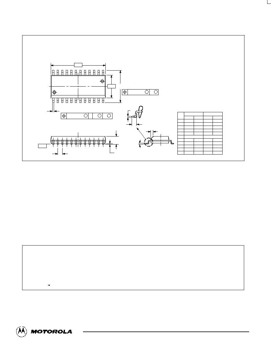
OUTLINE DIMENSIONS
J SUFFIX
CERAMIC PACKAGE
CASE 75802
ISSUE A
NOTES:
1. CHAMFERED CONTOUR OPTIONAL.
2. DIMENSION L TO CENTER OF LEADS WHEN
FORMED PARALLEL.
3. DIMENSIONING AND TOLERANCING PER ANSI
Y14.5M, 1982.
4. CONTROLLING DIMENSION: INCH.
A
B
24
13
12
1
T
SEATING
PLANE
24 PL
K
E
F
N
C
D
G
M
A
M
0.25 (0.010)
T
24 PL
J
M
B
M
0.25 (0.010)
T
L
M
NOTE 1
DIM
MIN
MAX
MIN
MAX
MILLIMETERS
INCHES
A
1.230
1.265
31.25
32.13
B
0.250
0.270
6.35
6.85
C
0.145
0.175
3.69
4.44
D
0.015
0.020
0.38
0.51
E
0.050 BSC
1.27 BSC
F
0.040
0.060
1.02
1.52
G
0.100 BSC
2.54 BSC
J
0.007
0.012
0.18
0.30
K
0.110
0.140
2.80
3.55
L
0.300 BSC
7.62 BSC
M
0
15
0
15
N
0.020
0.040
0.51
1.01
_
_
_
_
N SUFFIX
PLASTIC PACKAGE
CASE 72403
ISSUE D
C
N
K
F
G
B
1
24
12
13
L
P
J
SEATING
PLANE
DIM
A
MIN
MAX
MIN
MAX
MILLIMETERS
1.240
1.285
31.50
32.64
INCHES
B
0.285
0.305
7.24
7.75
C
0.160
0.200
4.07
5.08
D
0.015
0.021
0.38
0.53
F
0.045
0.062
1.14
1.57
G
0.100 BSC
2.54 BSC
J
0.008
0.013
0.20
0.33
K
0.100
0.165
2.54
4.19
L
0.300
0.310
7.62
7.87
N
0.020
0.050
0.51
1.27
P
0.360
0.400
9.14
10.16
NOTES:
3.
DIMENSIONING AND TOLERANCING PER ANSI
Y14.5M, 1982.
4.
CONTROLLING DIMENSION: INCH.
5.
DIMENSION L TO CENTER OF LEADS WHEN
FORMED PARALLEL.
0.25 (0.010)
M
T A
M
D
24 PL
T
A
MC54/74HC646
MOTOROLA
HighSpeed CMOS Logic Data
DL129 -- Rev 6
314
OUTLINE DIMENSIONS
DW SUFFIX
PLASTIC SOIC PACKAGE
CASE 751E04
ISSUE E
NOTES:
1. DIMENSIONING AND TOLERANCING PER ANSI
Y14.5M, 1982.
2. CONTROLLING DIMENSION: MILLIMETER.
3. DIMENSIONS A AND B DO NOT INCLUDE
MOLD PROTRUSION.
4. MAXIMUM MOLD PROTRUSION 0.15 (0.006)
PER SIDE.
5. DIMENSION D DOES NOT INCLUDE DAMBAR
PROTRUSION. ALLOWABLE DAMBAR
PROTRUSION SHALL BE 0.13 (0.005) TOTAL IN
EXCESS OF D DIMENSION AT MAXIMUM
MATERIAL CONDITION.
A
B
P
12X
D
24X
12
13
24
1
M
0.010 (0.25)
B
M
S
A
M
0.010 (0.25)
B
S
T
T
G
22X
SEATING
PLANE
K
C
R
X 45
_
M
F
J
DIM
MIN
MAX
MIN
MAX
INCHES
MILLIMETERS
A
15.25
15.54
0.601
0.612
B
7.40
7.60
0.292
0.299
C
2.35
2.65
0.093
0.104
D
0.35
0.49
0.014
0.019
F
0.41
0.90
0.016
0.035
G
1.27 BSC
0.050 BSC
J
0.23
0.32
0.009
0.013
K
0.13
0.29
0.005
0.011
M
0
8
0
8
P
10.05
10.55
0.395
0.415
R
0.25
0.75
0.010
0.029
_
_
_
_
How to reach us:
USA/EUROPE: Motorola Literature Distribution;
JAPAN: Nippon Motorola Ltd.; TatsumiSPDJLDC, Toshikatsu Otsuki,
P.O. Box 20912; Phoenix, Arizona 85036. 18004412447
6F SeibuButsuryuCenter, 3142 Tatsumi KotoKu, Tokyo 135, Japan. 0335218315
MFAX: RMFAX0@email.sps.mot.com TOUCHTONE (602) 2446609
HONG KONG: Motorola Semiconductors H.K. Ltd.; 8B Tai Ping Industrial Park,
INTERNET: http://DesignNET.com
51 Ting Kok Road, Tai Po, N.T., Hong Kong. 85226629298
Motorola reserves the right to make changes without further notice to any products herein. Motorola makes no warranty, representation or guarantee regarding
the suitability of its products for any particular purpose, nor does Motorola assume any liability arising out of the application or use of any product or circuit,
and specifically disclaims any and all liability, including without limitation consequential or incidental damages. "Typical" parameters can and do vary in different
applications. All operating parameters, including "Typicals" must be validated for each customer application by customer's technical experts. Motorola does
not convey any license under its patent rights nor the rights of others. Motorola products are not designed, intended, or authorized for use as components in
systems intended for surgical implant into the body, or other applications intended to support or sustain life, or for any other application in which the failure of
the Motorola product could create a situation where personal injury or death may occur. Should Buyer purchase or use Motorola products for any such
unintended or unauthorized application, Buyer shall indemnify and hold Motorola and its officers, employees, subsidiaries, affiliates, and distributors harmless
against all claims, costs, damages, and expenses, and reasonable attorney fees arising out of, directly or indirectly, any claim of personal injury or death
associated with such unintended or unauthorized use, even if such claim alleges that Motorola was negligent regarding the design or manufacture of the part.
Motorola and
are registered trademarks of Motorola, Inc. Motorola, Inc. is an Equal Opportunity/Affirmative Action Employer.
MC54/74HC646/D
*MC54/74HC646/D*
CODELINE