© Motorola, Inc., 2003
HC908JB8AD/D
Rev. 0, 4/2002
Addendum to
MC68HC908JB8
Technical Data
Addendum
This addendum provides additional information to the
MC68HC908JB8 Technical Data, Rev. 2
(Motorola document number MC68HC908JB8/D),
MC68HC08JB8A
The MC68HC08JB8A is the ROM part equivalent to the MC68HC908JB8. The
entire MC68HC908JB8 data book apply to this ROM device, with exceptions
outlined in this addendum.
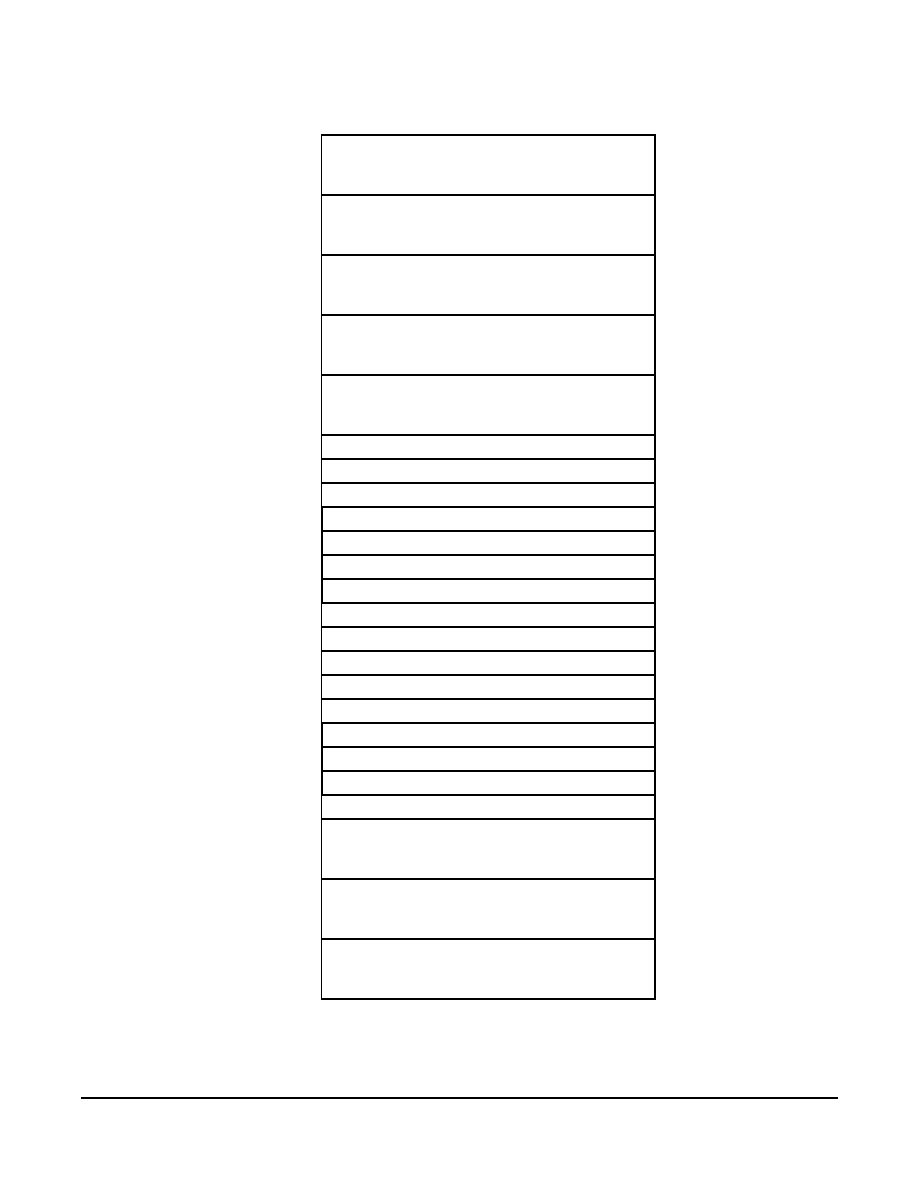
MCU Block Diagram
Figure 1
shows the block diagram of the MC68HC08JB8A.
Memory Map
The MC68HC08JB8A has 8,192 bytes of user ROM from $DC00 to $FBFF, and
16 bytes of user ROM vectors from $FFF0 to $FFFF. On the MC68HC908JB8,
these memory locations are FLASH memory.
Figure 2
shows the memory map of the MC68HC08JB8A.
Table 1. Summary of MC68HC08JB8A and MC68HC908JB8 Differences
MC68HC08JB8A
MC68HC908JB8
Memory ($DC00≠$FBFF)
8,192 bytes ROM
8,192 bytes FLASH
User vectors ($FFF0≠$FFFF)
16 bytes ROM
16 bytes FLASH
Registers at $FE08 and $FF09
Not used;
locations are reserved.
FLASH related registers.
$FE08 -- FLCR
$FF09 -- FLBPR
Monitor ROM
($FC00≠$FDFF and $FE10≠$FFDF)
$FC00≠$FDFF: Not used.
$FE10≠$FFDF: Used for
testing purposes only.
Used for testing and FLASH
programming/erasing.
OSC1 and OSC2 pins
V
DD
level (5V logic)
V
REG
level (3.3V logic)

HC908JB8AD/D
2
Addendum to MC68HC908JB8 Technical Data
MOTOROLA
Fi
gure 1. MC68HC08JB8A
Bl
ock D
i
agr
a
m
SY
ST
E
M
I
N
T
E
G
R
A
T
IO
N
MO
DU
L
E
T
I
ME
R I
N
TE
RF
AC
E
MO
DU
LE
L
O
W
VO
LT
AG
E I
N
HI
BI
T
MO
DU
LE
CO
MP
UT
ER
OP
ER
A
T
I
N
G
PR
OP
ER
L
Y
MO
DU
LE
AR
IT
H
M
E
T
I
C
/L
O
G
I
C
U
N
IT
(A
LU
)
CP
U
RE
GI
S
T
E
R
S
M6
8H
C08
CP
U
C
O
N
T
R
O
L
AN
D S
T
AT
US
RE
GI
STE
R
S
--
64
BY
TES
US
ER
RO
M --
8
,
19
2 B
Y
T
E
S
US
ER
RA
M --
2
5
6
B
Y
T
E
S
MO
NIT
O
R
RO
M --
4
64
BYT
ES
U
SER
R
O
M
VE
CT
ORS
--
16
BY
TE
S
IRQ
MO
DU
L
E
PO
WE
R
PTA
DDRA
DDRE
PTE
I
N
TE
RN
AL
BU
S
(1
)
OS
C1
(1
)
OS
C2
(1
), (
2
)
RS
T
(
1
), (3)
IR
Q
V
DD
V
SS
PT
A
7
/
K
BA
7
(3
)
PT
E4/
D
≠
(
3
) (4
) (
5
)
PT
E3/
D
+
(3
) (
4
)
(5
)
PT
E2/
T
CH
1
(3
)
PT
E1/
T
CH
0
(3
)
PT
E0
/
T
C
L
K
(3
)
PTB
DDRB
PT
B
7
≠PT
B
0
(3
)
PTD
DDRD
PT
D
5
≠PT
D
2
(
4
)
(5
)
US
B
MO
DU
L
E
U
S
B
EN
DPO
I
N
T
0
,
1,
2
IN
TE
RN
AL VO
LTA
G
E
RE
GU
LA
TOR
V
RE
G
(3.3
V)
(1)
P
ins have 5
V
logic.
(2)
P
ins have i
n
t
egrat
ed
pu
l
l
up device.
(3)
P
ins have sof
t
ware conf
igurable
pull-up device.
(4)
P
ins
are op
en-drain w
hen c
onf
igured
as
out
put
.
(5)
P
ins have 10
m
A
sink capabilit
y.
(6)
P
ins have 25
m
A
sink capabilit
y.
LS US
B
TR
ANSC
EIV
ER
BR
EA
K
MO
DU
LE
OS
CI
LLA
TO
R
PTC
DDRC
PT
C
7
≠PT
C
0
(3
)
KE
YBO
A
R
D
INT
E
RR
UP
T
MO
DU
LE
PO
WE
R-O
N
R
E
S
E
T
MO
DU
LE
PT
D
7
≠PT
D
6
(4
)
PT
D
1
≠PT
D
0
(
4
)
(6
)
PT
A
0
/
K
BA
0
(3
)
:
S
haded bl
oc
ks indicat
e
dif
f
erenc
es t
o
MC68HC
908JB8
HC908JB8AD/D
MC68HC08JB8A
MOTOROLA
Addendum to MC68HC908JB8 Technical Data
3
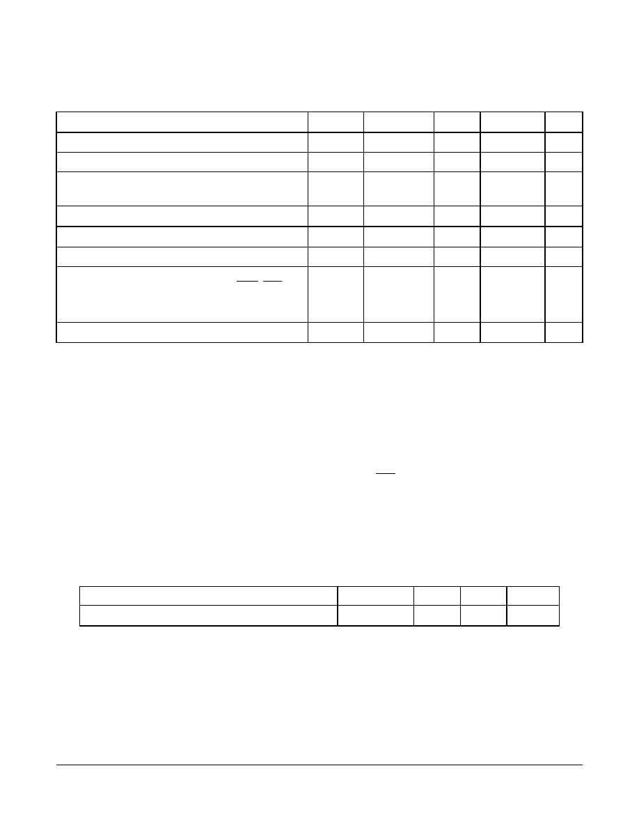
$0000
$003F
I/O Registers
64 Bytes
$0040
$013F
RAM
256 Bytes
$0140
$DBFF
Unimplemented
56,000 Bytes
$DC00
$FBFF
ROM
8,192 Bytes
$FC00
$FDFF
Unimplemented
512 Bytes
$FE00
Break Status Register (BSR)
$FE01
Reset Status Register (RSR)
$FE02
Reserved
$FE03
Break Flag Control Register (BFCR)
$FE04
Interrupt Status Register 1 (INT1)
$FE05
Reserved
$FE06
Reserved
$FE07
Reserved
$FE08
Reserved
$FE09
Reserved
$FE0A
Reserved
$FE0B
Reserved
$FE0C
Break Address High Register (BRKH)
$FE0D
Break Address Low Register (BRKL)
$FE0E
Break Status and Control Register (BRKSCR)
$FE0F
Reserved
$FE10
$FFDF
Monitor ROM
464 Bytes
$FFE0
$FFEF
Reserved
16 Bytes
$FFF0
$FFFF
ROM Vectors
16 Bytes
Figure 2. MC68HC08JB8A Memory Map

HC908JB8AD/D
4
Addendum to MC68HC908JB8 Technical Data
MOTOROLA
Reserved Registers
The two registers at $FE08 and $FE09 are reserved locations on the
MC68HC08JB8A.
On the MC68HC908JB8, these two locations are the FLASH control register
and the FLASH block protect register respectively.
Monitor ROM
The monitor program (monitor ROM: $FE10≠$FFDF) on the MC68HC08JB8A
is for device testing only. $FC00≠$FDFF are unused.
Electrical
Specifications
Electrical specifications for the MC68HC908JB8 apply to the MC68HC08JB8A,
except for the parameters indicated below.
DC Electrical
Characteristics
Table 2. DC Electrical Characteristics
Characteristic
(1)
Symbol
Min
Typ
(2)
Max
Unit
Regulator output voltage
V
REG
3.0
3.3
3.6
V
Output high voltage (I
Load
= ≠2.0 mA)
PTA0≠PTA7, PTB0≠PTB7, PTC0≠PTC7,
PTE0≠PTE2
V
OH
V
REG
≠0.8
--
--
V
Output low voltage
(I
Load
= 1.6 mA) All I/O pins
(I
Load
= 25 mA) PTD0≠PTD1 in ILDD mode
(I
Load
= 10 mA) PTE3≠PTE4 with USB disabled
V
OL
--
--
--
--
--
--
0.4
0.5
0.4
V
Input high voltage
All ports, OSC1
IRQ, RST
V
IH
0.7
◊
V
REG
0.7
◊
V
DD
--
--
V
REG
V
DD
V
Input low voltage
All ports, OSC1
IRQ, RST
V
IL
V
SS
V
SS
--
--
0.3
◊
V
REG
0.3
◊
V
DD
V
Output low current (V
OL
= 2.0 V)
PTD2≠PTD5 in LDD mode
I
OL
12 (17) 1
7 (22) 22 (27) mA
V
DD
supply current, V
DD
= 5.25V, f
OP
= 3MHz
Run, with low speed USB
(3)
Run, with USB suspended
(3)
Wait, with low speed USB
(4)
Wait, with USB suspended
(4)
Stop
(5)
0
∞C to 70∞C
I
DD
--
--
--
--
--
6.0 (5.0)
5.5 (4.5)
4.0 (3.0)
3.0 (2.5)
30
7.5
6.5
5.0
4.0
100
mA
mA
mA
mA
µA
HC908JB8AD/D
MC68HC08JB8A
MOTOROLA
Addendum to MC68HC908JB8 Technical Data
5
Memory
Characteristics
I/O ports Hi-Z leakage current
I
IL
--
--
± 10
µA
Input current
I
IN
--
--
± 1
µA
Capacitance
Ports (as input or output)
C
Out
C
In
--
--
--
--
12
8
pF
POR re-arm voltage
(6)
V
POR
0
--
100
mV
POR rise-time ramp rate
(7)
R
POR
0.035
--
--
V/ms
Monitor mode entry voltage
V
DD
+
V
HI
1.4
◊
V
DD
2
◊
V
DD
V
Pullup resistors
Port A, port B, port C, PTE0≠PTE2, RST, IRQ
PTE3≠PTE4 (with USB module disabled)
D≠ (with USB module enabled)
R
PU
25
4
1.2
40
5
1.5
55
6
2.0
k
LVI reset
V
LVR
2.8 (2.4)
3.3 (2.7)
3.8 (3.0)
(8)
V
1. V
DD
= 4.0 to 5.5 Vdc, V
SS
= 0 Vdc, T
A
= T
L
to T
H
, unless otherwise noted.
2. Typical values reflect average measurements at midpoint of voltage range, 25
∞C only.
3. Run (operating) I
DD
measured using external square wave clock source (f
XCLK
= 6 MHz). All inputs 0.2 V from rail. No dc
loads. Less than 100 pF on all outputs. C
L
= 20 pF on OSC2. All ports configured as inputs. OSC2 capacitance linearly
affects run I
DD
. Measured with all modules enabled.
4. Wait I
DD
measured using external square wave clock source (f
XCLK
= 6 MHz); all inputs 0.2 V from rail; no dc loads; less
than 100 pF on all outputs. C
L
= 20 pF on OSC2; 15 k
± 5% termination resistors on D+ and D≠ pins; all ports configured
as inputs; OSC2 capacitance linearly affects wait I
DD
5. STOP I
DD
measured with USB in suspend mode; OSC1 grounded; transceiver pullup resistor of 1.5 k
± 5% between V
REG
and D≠ pins and 15 k
± 5% termination resistor on D+ pin; no port pins sourcing current.
6. Maximum is highest voltage that POR is guaranteed.
7. If minimum V
REG
is not reached before the internal POR reset is released, RST must be driven low externally until minimum
V
REG
is reached.
8. The numbers in parenthesis are MC68HC08JB8 (non-A part) values.
Table 2. DC Electrical Characteristics
Characteristic
(1)
Symbol
Min
Typ
(2)
Max
Unit
Table 3. Memory Characteristics
Characteristic
Symbol
Min
Max
Unit
RAM data retention voltage
V
RDR
1.3
--
V
Notes:
Since MC68HC08JB8A is a ROM device, FLASH memory electrical characteristics do not apply.

HC908JB8AD/D
6
Addendum to MC68HC908JB8 Technical Data
MOTOROLA
MC68HC08JB8A
Order Numbers
These part numbers are generic numbers only. To place an order, ROM code
must be submitted to the ROM Processing Center (RPC).
MC68HC08JB8A and MC68HC08JB8 Differences
The MC68HC08JB8A and MC68HC08JB8 are identical devices, except for the
following:
Table 4. MC68HC08JB8A Order Numbers
MC order number
Package
Operating
temperature range
MC68HC08JB8AJP
20-pin PDIP
0
∞C to +70 ∞C
MC68HC08JB8AJDW
20-pin SOIC
0
∞C to +70 ∞C
MC68HC08JB8AADW
28-pin SOIC
0
∞C to +70 ∞C
MC68HC08JB8AFB
44-pin QFP
0
∞C to +70 ∞C
Table 5. MC68HC08JB8A and MC68HC08JB8 Differences
MC68HC08JB8A
MC68HC08JB8
OSC1 and OSC2 pins
V
DD
level (5V logic)
V
REG
level (3.3V logic)
Output low current on PTD2≠PTD5
in LDD mode
See
Table 2 . DC Electrical Characteristics
.
The numbers in parenthesis are MC68HC08JB8 values.
Operating I
DD
currents
LVI trip points

HC908JB8AD/D
NOTES
MOTOROLA
Addendum to MC68HC908JB8 Technical Data
7
NOTES

Information in this document is provided solely to enable system and software
implementers to use Motorola products. There are no express or implied copyright
licenses granted hereunder to design or fabricate any integrated circuits or
integrated circuits based on the information in this document.
Motorola reserves the right to make changes without further notice to any products
herein. Motorola makes no warranty, representation or guarantee regarding the
suitability of its products for any particular purpose, nor does Motorola assume any
liability arising out of the application or use of any product or circuit, and specifically
disclaims any and all liability, including without limitation consequential or incidental
damages. "Typical" parameters which may be provided in Motorola data sheets
and/or specifications can and do vary in different applications and actual
performance may vary over time. All operating parameters, including "Typicals"
must be validated for each customer application by customer's technical experts.
Motorola does not convey any license under its patent rights nor the rights of
others. Motorola products are not designed, intended, or authorized for use as
components in systems intended for surgical implant into the body, or other
applications intended to support or sustain life, or for any other application in which
the failure of the Motorola product could create a situation where personal injury or
death may occur. Should Buyer purchase or use Motorola products for any such
unintended or unauthorized application, Buyer shall indemnify and hold Motorola
and its officers, employees, subsidiaries, affiliates, and distributors harmless
against all claims, costs, damages, and expenses, and reasonable attorney fees
arising out of, directly or indirectly, any claim of personal injury or death associated
with such unintended or unauthorized use, even if such claim alleges that Motorola
was negligent regarding the design or manufacture of the part.
Motorola and the Stylized M Logo are registered in the U.S. Patent and Trademark
Office. digital dna is a trademark of Motorola, Inc. All other product or service
names are the property of their respective owners. Motorola, Inc. is an Equal
Opportunity/Affirmative Action Employer.
© Motorola, Inc. 2003
HC908JB8AD/D
Rev. 0
4/2003
HOW TO REACH US:
USA/EUROPE/LOCATIONS NOT LISTED:
Motorola Literature Distribution
P.O. Box 5405, Denver, Colorado 80217
1-800-521-6274 or 480-768-2130
JAPAN:
Motorola Japan Ltd.; SPS, Technical Information Center
3-20-1, Minami-Azabu Minato-ku, Tokyo 106-8573 Japan
81-3-3440-3569
ASIA/PACIFIC:
Motorola Semiconductors H.K. Ltd.
Silicon Harbour Centre, 2 Dai King Street
Tai Po Industrial Estate, Tai Po, N.T., Hong Kong
852-26668334
HOME PAGE:
http://motorola.com/semiconductors