
MC68HC908RK2/D
REV 4
MC68HC908RK2
Advance Information
HCMOS
Microcontroller Unit
M
6
8
H
C
0
8
M
6
0
8M
6
8
H
C
0
8
M
8
HC
0
8
M6
8
H
C

blank

MC68HC908RK2 -- Rev. 4.0
Advance Information
MOTOROLA
3
MC68HC908RK2
Advance Information
Motorola reserves the right to make changes without further notice to any products
herein. Motorola makes no warranty, representation or guarantee regarding the
suitability of its products for any particular purpose, nor does Motorola assume any
liability arising out of the application or use of any product or circuit, and specifically
disclaims any and all liability, including without limitation consequential or incidental
damages. "Typical" parameters which may be provided in Motorola data sheets and/or
specifications can and do vary in different applications and actual performance may
vary over time. All operating parameters, including "Typicals" must be validated for
each customer application by customer's technical experts. Motorola does not convey
any license under its patent rights nor the rights of others. Motorola products are not
designed, intended, or authorized for use as components in systems intended for
surgical implant into the body, or other applications intended to support or sustain life,
or for any other application in which the failure of the Motorola product could create a
situation where personal injury or death may occur. Should Buyer purchase or use
Motorola products for any such unintended or unauthorized application, Buyer shall
indemnify and hold Motorola and its officers, employees, subsidiaries, affiliates, and
distributors harmless against all claims, costs, damages, and expenses, and
reasonable attorney fees arising out of, directly or indirectly, any claim of personal
injury or death associated with such unintended or unauthorized use, even if such claim
alleges that Motorola was negligent regarding the design or manufacture of the part.
Motorola, Inc. is an Equal Opportunity/Affirmative Action Employer.
Motorola and
are registered trademarks of Motorola, Inc.
DigitalDNA is a trademark of Motorola, Inc.
© Motorola, Inc., 2001

Advance Information
MC68HC908RK2 -- Rev. 4.0
4
MOTOROLA
Advance Information
To provide the most up-to-date information, the revision of our
documents on the World Wide Web will be the most current. Your printed
copy may be an earlier revision. To verify you have the latest information
available, refer to:
http://www.motorola.com/semiconductors/
The following revision history table summarizes changes contained in
this document. For your convenience, the page number designators
have been linked to the appropriate location.
Revision History
Date
Revision
Level
Description
Page
Number(s)
June,
2001
3
First bulleted paragraph under the subsection
15.6 Interrupts
reworded for clarity
205
Note to TOVx bit description deleted. Revision to the description
of the CHxMAX bit and the note that follows that description
214
16.11 LVI Characteristics
-- V
LVS
and V
LVR
specifications
updated
224
16.12 Memory Characteristics
-- Maximum value for FLASH
page program pulses updated
225
December,
2001
4
Section 15. Timer Interface Module (TIM)
-- Timer
discrepancies corrected throughout this section.
195

MC68HC908RK2 -- Rev. 4.0
Advance Information
MOTOROLA
List of Sections
5
Advance Information -- MC68HC908RK2
List of Sections
Section 1. General Description . . . . . . . . . . . . . . . . . . . . 23
Section 2. Memory Map . . . . . . . . . . . . . . . . . . . . . . . . . . 31
Section 3. Random-Access Memory (RAM) . . . . . . . . . . 41
Section 4. FLASH 2TS Memory . . . . . . . . . . . . . . . . . . . . 43
Section 5. Central Processor Unit (CPU) . . . . . . . . . . . . 63
Section 6. System Integration Module (SIM) . . . . . . . . . 79
Section 7. Break Module (BRK) . . . . . . . . . . . . . . . . . . . 101
Section 8. Internal Clock Generator Module (ICG) . . . . 107
Section 9. Configuration Register (CONFIG) . . . . . . . . 145
Section 10. Monitor Read-Only Memory (MON) . . . . . . 149
Section 11. Computer Operating Properly
Module (COP) . . . . . . . . . . . . . . . . . . . . . . . 161
Section 12. Low-Voltage Inhibit (LVI) . . . . . . . . . . . . . . 167
Section 13. Input/Output (I/O) Ports . . . . . . . . . . . . . . . 173
Section 14. Keyboard/External Interrupt
Module (KBI) . . . . . . . . . . . . . . . . . . . . . . . . 181
Section 15. Timer Interface Module (TIM) . . . . . . . . . . . 195
Section 16. Preliminary Electrical Specifications . . . . 217
Section 17. Mechanical Specifications . . . . . . . . . . . . . 227
Section 18. Ordering Information . . . . . . . . . . . . . . . . . 229

Advance Information
MC68HC908RK2 -- Rev. 4.0
6
List of Sections
MOTOROLA
List of Sections

MC68HC908RK2 -- Rev. 4.0
Advance Information
MOTOROLA
Table of Contents
7
Advance Information -- MC68HC908RK2
Table of Contents
Section 1. General Description
1.1
Contents . . . . . . . . . . . . . . . . . . . . . . . . . . . . . . . . . . . . . . . . . . 23
1.2
Introduction . . . . . . . . . . . . . . . . . . . . . . . . . . . . . . . . . . . . . . . . 23
1.3
Features . . . . . . . . . . . . . . . . . . . . . . . . . . . . . . . . . . . . . . . . . . 24
1.4
MCU Block Diagram . . . . . . . . . . . . . . . . . . . . . . . . . . . . . . . . . 25
1.5
Pin Assignments . . . . . . . . . . . . . . . . . . . . . . . . . . . . . . . . . . . . 27
1.5.1
Power Supply Pins (V
DD
and V
SS
) . . . . . . . . . . . . . . . . . . . .27
1.5.2
Oscillator Pins (OSC1 and OSC2) . . . . . . . . . . . . . . . . . . . .28
1.5.3
External Reset (RST) . . . . . . . . . . . . . . . . . . . . . . . . . . . . . . 28
1.5.4
External Interrupt Pin (IRQ1) . . . . . . . . . . . . . . . . . . . . . . . .28
1.5.5
Port A Input/Output Pins
(PTA7, PTA6/KBD6≠PTA1/KBD1, and PTA0) . . . . . . . . 29
1.5.6
Port B Input/Output Pins (PTB5, PTB4/TCH1,
PTB3/TCLK, PTB2/TCH0, PTB1, and PTB0/MCLK). . . . 29
Section 2. Memory Map
2.1
Contents . . . . . . . . . . . . . . . . . . . . . . . . . . . . . . . . . . . . . . . . . . 31
2.2
Introduction . . . . . . . . . . . . . . . . . . . . . . . . . . . . . . . . . . . . . . . . 31
2.3
Input/Output Section . . . . . . . . . . . . . . . . . . . . . . . . . . . . . . . . . 33
2.4
Monitor ROM . . . . . . . . . . . . . . . . . . . . . . . . . . . . . . . . . . . . . .40
Section 3. Random-Access Memory (RAM)
3.1
Contents . . . . . . . . . . . . . . . . . . . . . . . . . . . . . . . . . . . . . . . . . . 41
3.2
Introduction . . . . . . . . . . . . . . . . . . . . . . . . . . . . . . . . . . . . . . . . 41
3.3
Functional Description . . . . . . . . . . . . . . . . . . . . . . . . . . . . . . . 41

Advance Information
MC68HC908RK2 -- Rev. 4.0
8
Table of Contents
MOTOROLA
Table of Contents
Section 4. FLASH 2TS Memory
4.1
Contents . . . . . . . . . . . . . . . . . . . . . . . . . . . . . . . . . . . . . . . . . . 43
4.2
Introduction . . . . . . . . . . . . . . . . . . . . . . . . . . . . . . . . . . . . . . . . 43
4.3
Functional Description . . . . . . . . . . . . . . . . . . . . . . . . . . . . . . . 44
4.4
FLASH 2TS Control Register . . . . . . . . . . . . . . . . . . . . . . . . . . 45
4.5
FLASH 2TS Charge Pump Frequency Control. . . . . . . . . . . . . 47
4.6
FLASH 2TS Erase Operation . . . . . . . . . . . . . . . . . . . . . . . . . . 47
4.7
FLASH 2TS Program/Margin Read Operation . . . . . . . . . . . . . 48
4.8
FLASH 2TS Block Protection . . . . . . . . . . . . . . . . . . . . . . . . . . 51
4.9
FLASH 2TS Block Protect Register . . . . . . . . . . . . . . . . . . . . . 52
4.10
Embedded Program/Erase Routines . . . . . . . . . . . . . . . . . . . . 53
4.11
Embedded Function Descriptions. . . . . . . . . . . . . . . . . . . . . . . 54
4.11.1
RDVRRNG Routine . . . . . . . . . . . . . . . . . . . . . . . . . . . . . . . 54
4.11.2
PRGRNGE Routine . . . . . . . . . . . . . . . . . . . . . . . . . . . . . . . 55
4.11.3
ERARNGE Routine . . . . . . . . . . . . . . . . . . . . . . . . . . . . . . . 56
4.11.4
REDPROG Routine . . . . . . . . . . . . . . . . . . . . . . . . . . . . . . . 57
4.11.5
Example Routine Calls . . . . . . . . . . . . . . . . . . . . . . . . . . . . .58
4.12
Low-Power Modes . . . . . . . . . . . . . . . . . . . . . . . . . . . . . . . . . . 60
4.12.1
Wait Mode . . . . . . . . . . . . . . . . . . . . . . . . . . . . . . . . . . . . . .60
4.12.2
Stop Mode . . . . . . . . . . . . . . . . . . . . . . . . . . . . . . . . . . . . . .61
Section 5. Central Processor Unit (CPU)
5.1
Contents . . . . . . . . . . . . . . . . . . . . . . . . . . . . . . . . . . . . . . . . . . 63
5.2
Introduction . . . . . . . . . . . . . . . . . . . . . . . . . . . . . . . . . . . . . . . . 64
5.3
Features . . . . . . . . . . . . . . . . . . . . . . . . . . . . . . . . . . . . . . . . . . 64
5.4
CPU Registers . . . . . . . . . . . . . . . . . . . . . . . . . . . . . . . . . . . . . 64
5.4.1
Accumulator . . . . . . . . . . . . . . . . . . . . . . . . . . . . . . . . . . . . . 65
5.4.2
Index Register . . . . . . . . . . . . . . . . . . . . . . . . . . . . . . . . . . . 65
5.4.3
Stack Pointer . . . . . . . . . . . . . . . . . . . . . . . . . . . . . . . . . . . . 66
5.4.4
Program Counter . . . . . . . . . . . . . . . . . . . . . . . . . . . . . . . . .67
5.4.5
Condition Code Register . . . . . . . . . . . . . . . . . . . . . . . . . . . 67

Table of Contents
MC68HC908RK2 -- Rev. 4.0
Advance Information
MOTOROLA
Table of Contents
9
5.5
Arithmetic/Logic Unit (ALU) . . . . . . . . . . . . . . . . . . . . . . . . . . . 69
5.6
Low-Power Modes . . . . . . . . . . . . . . . . . . . . . . . . . . . . . . . . . . 69
5.6.1
Wait Mode . . . . . . . . . . . . . . . . . . . . . . . . . . . . . . . . . . . . . .70
5.6.2
Stop Mode . . . . . . . . . . . . . . . . . . . . . . . . . . . . . . . . . . . . . .70
5.7
CPU During Break Interrupts . . . . . . . . . . . . . . . . . . . . . . . . . . 70
5.8
Instruction Set Summary . . . . . . . . . . . . . . . . . . . . . . . . . . . . . 70
5.9
Opcode Map . . . . . . . . . . . . . . . . . . . . . . . . . . . . . . . . . . . . . . . 77
Section 6. System Integration Module (SIM)
6.1
Contents . . . . . . . . . . . . . . . . . . . . . . . . . . . . . . . . . . . . . . . . . . 79
6.2
Introduction . . . . . . . . . . . . . . . . . . . . . . . . . . . . . . . . . . . . . . . . 80
6.3
SIM Bus Clock Control and Generation . . . . . . . . . . . . . . . . . . 83
6.3.1
Bus Timing . . . . . . . . . . . . . . . . . . . . . . . . . . . . . . . . . . . . . .83
6.3.2
Clock Startup from POR or LVI Reset . . . . . . . . . . . . . . . . . 83
6.3.3
Clocks in Stop Mode and Wait Mode . . . . . . . . . . . . . . . . . . 84
6.4
Reset and System Initialization. . . . . . . . . . . . . . . . . . . . . . . . . 84
6.4.1
External Pin Reset . . . . . . . . . . . . . . . . . . . . . . . . . . . . . . . . 85
6.4.2
Active Resets from Internal Sources . . . . . . . . . . . . . . . . . . 86
6.4.2.1
Power-On Reset . . . . . . . . . . . . . . . . . . . . . . . . . . . . . . . 87
6.4.2.2
Computer Operating Properly (COP) Reset. . . . . . . . . . . 88
6.4.2.3
Illegal Opcode Reset . . . . . . . . . . . . . . . . . . . . . . . . . . . . 88
6.4.2.4
Illegal Address Reset . . . . . . . . . . . . . . . . . . . . . . . . . . . . 88
6.4.2.5
Low-Voltage Inhibit (LVI) Reset . . . . . . . . . . . . . . . . . . . .88
6.5
SIM Counter . . . . . . . . . . . . . . . . . . . . . . . . . . . . . . . . . . . . . . . 89
6.5.1
SIM Counter During Power-On Reset . . . . . . . . . . . . . . . . . 89
6.5.2
SIM Counter During Stop Mode Recovery . . . . . . . . . . . . . . 89
6.5.3
SIM Counter and Reset States. . . . . . . . . . . . . . . . . . . . . . . 89
6.6
Program Exception Control. . . . . . . . . . . . . . . . . . . . . . . . . . . . 90
6.6.1
Interrupts . . . . . . . . . . . . . . . . . . . . . . . . . . . . . . . . . . . . . . . 90
6.6.1.1
Hardware Interrupts . . . . . . . . . . . . . . . . . . . . . . . . . . . . .92
6.6.1.2
SWI Instruction. . . . . . . . . . . . . . . . . . . . . . . . . . . . . . . . . 93
6.6.2
Reset . . . . . . . . . . . . . . . . . . . . . . . . . . . . . . . . . . . . . . . . . . 93
6.6.3
Break Interrupts . . . . . . . . . . . . . . . . . . . . . . . . . . . . . . . . . . 93
6.6.4
Status Flag Protection in Break Mode . . . . . . . . . . . . . . . . . 94

Advance Information
MC68HC908RK2 -- Rev. 4.0
10
Table of Contents
MOTOROLA
Table of Contents
6.7
Low-Power Modes . . . . . . . . . . . . . . . . . . . . . . . . . . . . . . . . . . 94
6.7.1
Wait Mode . . . . . . . . . . . . . . . . . . . . . . . . . . . . . . . . . . . . . .94
6.7.2
Stop Mode . . . . . . . . . . . . . . . . . . . . . . . . . . . . . . . . . . . . . .96
6.8
SIM Registers . . . . . . . . . . . . . . . . . . . . . . . . . . . . . . . . . . . . . .97
6.8.1
SIM Break Status Register . . . . . . . . . . . . . . . . . . . . . . . . . . 97
6.8.2
SIM Reset Status Register . . . . . . . . . . . . . . . . . . . . . . . . . 98
6.8.3
SIM Break Flag Control Register . . . . . . . . . . . . . . . . . . . . . 99
Section 7. Break Module (BRK)
7.1
Contents . . . . . . . . . . . . . . . . . . . . . . . . . . . . . . . . . . . . . . . . . 101
7.2
Introduction . . . . . . . . . . . . . . . . . . . . . . . . . . . . . . . . . . . . . . . 101
7.3
Features . . . . . . . . . . . . . . . . . . . . . . . . . . . . . . . . . . . . . . . . . 101
7.4
Functional Description . . . . . . . . . . . . . . . . . . . . . . . . . . . . . . 102
7.4.1
Flag Protection During Break Interrupts . . . . . . . . . . . . . . . 103
7.4.2
CPU During Break Interrupts . . . . . . . . . . . . . . . . . . . . . . .103
7.4.3
TIM During Break Interrupts . . . . . . . . . . . . . . . . . . . . . . . . 104
7.4.4
COP During Break Interrupts . . . . . . . . . . . . . . . . . . . . . . .104
7.5
Low-Power Modes . . . . . . . . . . . . . . . . . . . . . . . . . . . . . . . . . 104
7.5.1
Wait Mode . . . . . . . . . . . . . . . . . . . . . . . . . . . . . . . . . . . . .104
7.5.2
Stop Mode . . . . . . . . . . . . . . . . . . . . . . . . . . . . . . . . . . . . .104
7.6
Break Module Registers . . . . . . . . . . . . . . . . . . . . . . . . . . . . . 104
7.6.1
Break Status and Control Register . . . . . . . . . . . . . . . . . . .105
7.6.2
Break Address Registers . . . . . . . . . . . . . . . . . . . . . . . . . . 106
Section 8. Internal Clock Generator Module (ICG)
8.1
Contents . . . . . . . . . . . . . . . . . . . . . . . . . . . . . . . . . . . . . . . . . 107
8.2
Introduction . . . . . . . . . . . . . . . . . . . . . . . . . . . . . . . . . . . . . . . 108
8.3
Features . . . . . . . . . . . . . . . . . . . . . . . . . . . . . . . . . . . . . . . . . 108
8.4
Functional Description . . . . . . . . . . . . . . . . . . . . . . . . . . . . . . 109
8.4.1
Clock Enable Circuit . . . . . . . . . . . . . . . . . . . . . . . . . . . . . . 109
8.4.2
Internal Clock Generator . . . . . . . . . . . . . . . . . . . . . . . . . . 111
8.4.2.1
Digitally Controlled Oscillator . . . . . . . . . . . . . . . . . . . . . 112
8.4.2.2
Modulo N Divider . . . . . . . . . . . . . . . . . . . . . . . . . . . . . . 112
8.4.2.3
Frequency Comparator . . . . . . . . . . . . . . . . . . . . . . . . . 112

Table of Contents
MC68HC908RK2 -- Rev. 4.0
Advance Information
MOTOROLA
Table of Contents
11
8.4.2.4
Digital Loop Filter . . . . . . . . . . . . . . . . . . . . . . . . . . . . . . 113
8.4.3
External Clock Generator . . . . . . . . . . . . . . . . . . . . . . . . . . 114
8.4.3.1
External Oscillator Amplifier . . . . . . . . . . . . . . . . . . . . . . 114
8.4.3.2
External Clock Input Path . . . . . . . . . . . . . . . . . . . . . . .115
8.4.4
Clock Monitor Circuit . . . . . . . . . . . . . . . . . . . . . . . . . . . . . 115
8.4.4.1
Clock Monitor Reference Generator . . . . . . . . . . . . . . . 116
8.4.4.2
Internal Clock Activity Detector . . . . . . . . . . . . . . . . . . . 119
8.4.4.3
External Clock Activity Detector . . . . . . . . . . . . . . . . . . .119
8.4.5
Clock Selection Circuit . . . . . . . . . . . . . . . . . . . . . . . . . . . .120
8.4.5.1
Clock Selection Switch. . . . . . . . . . . . . . . . . . . . . . . . . . 120
8.4.5.2
Clock Switching Circuit. . . . . . . . . . . . . . . . . . . . . . . . . . 121
8.5
Usage Notes . . . . . . . . . . . . . . . . . . . . . . . . . . . . . . . . . . . . . . 122
8.5.1
Switching Clock Sources . . . . . . . . . . . . . . . . . . . . . . . . . . 123
8.5.2
Enabling the Clock Monitor . . . . . . . . . . . . . . . . . . . . . . . . 124
8.5.3
Clock Monitor Interrupts . . . . . . . . . . . . . . . . . . . . . . . . . . . 125
8.5.4
Quantization Error in DCO Output . . . . . . . . . . . . . . . . . . . 125
8.5.4.1
Digitally Controlled Oscillator . . . . . . . . . . . . . . . . . . . . . 126
8.5.4.2
Binary Weighted Divider . . . . . . . . . . . . . . . . . . . . . . . . 126
8.5.4.3
Variable-Delay Ring Oscillator . . . . . . . . . . . . . . . . . . . . 127
8.5.4.4
Ring Oscillator Fine-Adjust Circuit . . . . . . . . . . . . . . . . . 127
8.5.5
Switching Internal Clock Frequencies . . . . . . . . . . . . . . . . 128
8.5.6
Nominal Frequency Settling Time . . . . . . . . . . . . . . . . . . . 129
8.5.6.1
Settling to Within 15 Percent . . . . . . . . . . . . . . . . . . . . . 129
8.5.6.2
Settling to Within 5 Percent . . . . . . . . . . . . . . . . . . . . . . 130
8.5.6.3
Total Settling Time . . . . . . . . . . . . . . . . . . . . . . . . . . . . . 130
8.5.7
Improving Settling Time . . . . . . . . . . . . . . . . . . . . . . . . . . . 131
8.5.8
Trimming Frequency on the Internal Clock Generator . . . . 133
8.6
Low-Power Modes . . . . . . . . . . . . . . . . . . . . . . . . . . . . . . . . . 135
8.6.1
Wait Mode . . . . . . . . . . . . . . . . . . . . . . . . . . . . . . . . . . . . .135
8.6.2
Stop Mode . . . . . . . . . . . . . . . . . . . . . . . . . . . . . . . . . . . . .135
8.7
Configuration Register Option . . . . . . . . . . . . . . . . . . . . . . . . 135
8.7.1
EXTSLOW . . . . . . . . . . . . . . . . . . . . . . . . . . . . . . . . . . . . .136
8.8
I/O Registers. . . . . . . . . . . . . . . . . . . . . . . . . . . . . . . . . . . . . . 136
8.8.1
ICG Control Register . . . . . . . . . . . . . . . . . . . . . . . . . . . . . 139
8.8.2
ICG Multiplier Register . . . . . . . . . . . . . . . . . . . . . . . . . . . .141
8.8.3
ICG Trim Register . . . . . . . . . . . . . . . . . . . . . . . . . . . . . . . 142

Advance Information
MC68HC908RK2 -- Rev. 4.0
12
Table of Contents
MOTOROLA
Table of Contents
8.8.4
ICG DCO Divider Register . . . . . . . . . . . . . . . . . . . . . . . . . 143
8.8.5
ICG DCO Stage Register . . . . . . . . . . . . . . . . . . . . . . . . . . 144
Section 9. Configuration Register (CONFIG)
9.1
Contents . . . . . . . . . . . . . . . . . . . . . . . . . . . . . . . . . . . . . . . . . 145
9.2
Introduction . . . . . . . . . . . . . . . . . . . . . . . . . . . . . . . . . . . . . . . 145
9.3
Functional Description . . . . . . . . . . . . . . . . . . . . . . . . . . . . . . 145
Section 10. Monitor Read-Only Memory (MON)
10.1
Contents . . . . . . . . . . . . . . . . . . . . . . . . . . . . . . . . . . . . . . . . . 149
10.2
Introduction . . . . . . . . . . . . . . . . . . . . . . . . . . . . . . . . . . . . . . . 149
10.3
Features . . . . . . . . . . . . . . . . . . . . . . . . . . . . . . . . . . . . . . . . . 150
10.4
Functional Description . . . . . . . . . . . . . . . . . . . . . . . . . . . . . . 150
10.4.1
Monitor Mode Entry . . . . . . . . . . . . . . . . . . . . . . . . . . . . . . 152
10.4.2
Data Format . . . . . . . . . . . . . . . . . . . . . . . . . . . . . . . . . . . . 153
10.4.3
Echoing . . . . . . . . . . . . . . . . . . . . . . . . . . . . . . . . . . . . . . . 154
10.4.4
Break Signal . . . . . . . . . . . . . . . . . . . . . . . . . . . . . . . . . . . . 154
10.4.5
Commands . . . . . . . . . . . . . . . . . . . . . . . . . . . . . . . . . . . . .155
10.4.6
Baud Rate . . . . . . . . . . . . . . . . . . . . . . . . . . . . . . . . . . . . .158
10.4.7
Security . . . . . . . . . . . . . . . . . . . . . . . . . . . . . . . . . . . . . . . 158
Section 11. Computer Operating Properly
Module (COP)
11.1
Contents . . . . . . . . . . . . . . . . . . . . . . . . . . . . . . . . . . . . . . . . . 161
11.2
Introduction . . . . . . . . . . . . . . . . . . . . . . . . . . . . . . . . . . . . . . . 162
11.3
Functional Description . . . . . . . . . . . . . . . . . . . . . . . . . . . . . . 162
11.4
I/O Signals . . . . . . . . . . . . . . . . . . . . . . . . . . . . . . . . . . . . . . . 163
11.4.1
CGMXCLK . . . . . . . . . . . . . . . . . . . . . . . . . . . . . . . . . . . . .163
11.4.2
STOP Instruction . . . . . . . . . . . . . . . . . . . . . . . . . . . . . . . .163
11.4.3
COPCTL Write . . . . . . . . . . . . . . . . . . . . . . . . . . . . . . . . . . 164
11.4.4
Power-On Reset . . . . . . . . . . . . . . . . . . . . . . . . . . . . . . . . .164
11.4.5
Internal Reset . . . . . . . . . . . . . . . . . . . . . . . . . . . . . . . . . . . 164
11.4.6
Reset Vector Fetch. . . . . . . . . . . . . . . . . . . . . . . . . . . . . . . 164

Table of Contents
MC68HC908RK2 -- Rev. 4.0
Advance Information
MOTOROLA
Table of Contents
13
11.4.7
COPD . . . . . . . . . . . . . . . . . . . . . . . . . . . . . . . . . . . . . . . . . 164
11.4.8
COPRS. . . . . . . . . . . . . . . . . . . . . . . . . . . . . . . . . . . . . . . . 164
11.5
COP Control Register . . . . . . . . . . . . . . . . . . . . . . . . . . . . . . . 165
11.6
Interrupts. . . . . . . . . . . . . . . . . . . . . . . . . . . . . . . . . . . . . . . . . 165
11.7
Monitor Mode . . . . . . . . . . . . . . . . . . . . . . . . . . . . . . . . . . . . .165
11.8
Low-Power Modes . . . . . . . . . . . . . . . . . . . . . . . . . . . . . . . . . 165
11.8.1
Wait Mode . . . . . . . . . . . . . . . . . . . . . . . . . . . . . . . . . . . . .165
11.8.2
Stop Mode . . . . . . . . . . . . . . . . . . . . . . . . . . . . . . . . . . . . .166
11.9
COP Module During Break Interrupts . . . . . . . . . . . . . . . . . . .166
Section 12. Low-Voltage Inhibit (LVI)
12.1
Contents . . . . . . . . . . . . . . . . . . . . . . . . . . . . . . . . . . . . . . . . . 167
12.2
Introduction . . . . . . . . . . . . . . . . . . . . . . . . . . . . . . . . . . . . . . . 167
12.3
Features . . . . . . . . . . . . . . . . . . . . . . . . . . . . . . . . . . . . . . . . . 168
12.4
Functional Description . . . . . . . . . . . . . . . . . . . . . . . . . . . . . . 168
12.4.1
False Trip Protection . . . . . . . . . . . . . . . . . . . . . . . . . . . . . 169
12.4.2
Short Stop Recovery Option. . . . . . . . . . . . . . . . . . . . . . . . 169
12.5
LVI Status Register. . . . . . . . . . . . . . . . . . . . . . . . . . . . . . . . .170
12.6
LVI Interrupts . . . . . . . . . . . . . . . . . . . . . . . . . . . . . . . . . . . . .170
12.7
Low-Power Modes . . . . . . . . . . . . . . . . . . . . . . . . . . . . . . . . . 170
12.7.1
Wait Mode . . . . . . . . . . . . . . . . . . . . . . . . . . . . . . . . . . . . .171
12.7.2
Stop Mode . . . . . . . . . . . . . . . . . . . . . . . . . . . . . . . . . . . . .171
Section 13. Input/Output (I/O) Ports
13.1
Contents . . . . . . . . . . . . . . . . . . . . . . . . . . . . . . . . . . . . . . . . . 173
13.2
Introduction . . . . . . . . . . . . . . . . . . . . . . . . . . . . . . . . . . . . . . . 173
13.3
Port A . . . . . . . . . . . . . . . . . . . . . . . . . . . . . . . . . . . . . . . . . . . 175
13.3.1
Port A Data Register . . . . . . . . . . . . . . . . . . . . . . . . . . . . . 175
13.3.2
Data Direction Register A . . . . . . . . . . . . . . . . . . . . . . . . . . 176
13.4
Port B . . . . . . . . . . . . . . . . . . . . . . . . . . . . . . . . . . . . . . . . . . . 178
13.4.1
Port B Data Register . . . . . . . . . . . . . . . . . . . . . . . . . . . . . 178
13.4.2
Data Direction Register B . . . . . . . . . . . . . . . . . . . . . . . . . 179

Advance Information
MC68HC908RK2 -- Rev. 4.0
14
Table of Contents
MOTOROLA
Table of Contents
Section 14. Keyboard/External Interrupt
Module (KBI)
14.1
Contents . . . . . . . . . . . . . . . . . . . . . . . . . . . . . . . . . . . . . . . . . 181
14.2
Introduction . . . . . . . . . . . . . . . . . . . . . . . . . . . . . . . . . . . . . . . 181
14.3
Features . . . . . . . . . . . . . . . . . . . . . . . . . . . . . . . . . . . . . . . . . 182
14.4
Functional Description . . . . . . . . . . . . . . . . . . . . . . . . . . . . . . 182
14.4.1
External Interrupt . . . . . . . . . . . . . . . . . . . . . . . . . . . . . . . .182
14.4.2
IRQ1 Pin. . . . . . . . . . . . . . . . . . . . . . . . . . . . . . . . . . . . . . . 186
14.4.3
KBI Module During Break Interrupts. . . . . . . . . . . . . . . . . . 187
14.4.4
Keyboard Interrupt Pins . . . . . . . . . . . . . . . . . . . . . . . . . . . 187
14.4.5
Keyboard Initialization . . . . . . . . . . . . . . . . . . . . . . . . . . . . 189
14.5
Low-Power Modes . . . . . . . . . . . . . . . . . . . . . . . . . . . . . . . . . 190
14.5.1
Wait Mode . . . . . . . . . . . . . . . . . . . . . . . . . . . . . . . . . . . . .190
14.5.2
Stop Mode . . . . . . . . . . . . . . . . . . . . . . . . . . . . . . . . . . . . .190
14.6
I/O Registers. . . . . . . . . . . . . . . . . . . . . . . . . . . . . . . . . . . . . . 191
14.6.1
IRQ and Keyboard Status and Control Register . . . . . . . . 191
14.6.2
Keyboard Interrupt Enable Register . . . . . . . . . . . . . . . . . . 193
Section 15. Timer Interface Module (TIM)
15.1
Contents . . . . . . . . . . . . . . . . . . . . . . . . . . . . . . . . . . . . . . . . . 195
15.2
Introduction . . . . . . . . . . . . . . . . . . . . . . . . . . . . . . . . . . . . . . . 196
15.3
Features . . . . . . . . . . . . . . . . . . . . . . . . . . . . . . . . . . . . . . . . . 196
15.4
Pin Name Conventions . . . . . . . . . . . . . . . . . . . . . . . . . . . . . . 196
15.5
Functional Description . . . . . . . . . . . . . . . . . . . . . . . . . . . . . . 197
15.5.1
TIM Counter Prescaler . . . . . . . . . . . . . . . . . . . . . . . . . . . .199
15.5.2
Input Capture . . . . . . . . . . . . . . . . . . . . . . . . . . . . . . . . . . . 199
15.5.3
Output Compare . . . . . . . . . . . . . . . . . . . . . . . . . . . . . . . . .199
15.5.4
Unbuffered Output Compare . . . . . . . . . . . . . . . . . . . . . . .200
15.5.5
Buffered Output Compare . . . . . . . . . . . . . . . . . . . . . . . . . 201
15.5.6
Pulse-Width Modulation (PWM) . . . . . . . . . . . . . . . . . . . . . 201
15.5.7
Unbuffered PWM Signal Generation . . . . . . . . . . . . . . . . . 202
15.5.8
Buffered PWM Signal Generation . . . . . . . . . . . . . . . . . . . 203
15.5.9
PWM Initialization. . . . . . . . . . . . . . . . . . . . . . . . . . . . . . . . 204

Table of Contents
MC68HC908RK2 -- Rev. 4.0
Advance Information
MOTOROLA
Table of Contents
15
15.6
Interrupts. . . . . . . . . . . . . . . . . . . . . . . . . . . . . . . . . . . . . . . . . 205
15.6.1
Low-Power Modes . . . . . . . . . . . . . . . . . . . . . . . . . . . . . . . 205
15.6.2
Wait Mode . . . . . . . . . . . . . . . . . . . . . . . . . . . . . . . . . . . . .206
15.6.3
Stop Mode . . . . . . . . . . . . . . . . . . . . . . . . . . . . . . . . . . . . .206
15.7
TIM During Break Interrupts . . . . . . . . . . . . . . . . . . . . . . . . . . 206
15.8
I/O Signals . . . . . . . . . . . . . . . . . . . . . . . . . . . . . . . . . . . . . . . 207
15.8.1
TIM Clock Pin (TCLK) . . . . . . . . . . . . . . . . . . . . . . . . . . . . 207
15.8.2
TIM Channel I/O Pins (TCH0 and TCH1) . . . . . . . . . . . . . .207
15.9
I/O Registers. . . . . . . . . . . . . . . . . . . . . . . . . . . . . . . . . . . . . . 208
15.9.1
TIM Status and Control Register . . . . . . . . . . . . . . . . . . . . 208
15.9.2
TIM Counter Registers . . . . . . . . . . . . . . . . . . . . . . . . . . . .210
15.9.3
TIM Counter Modulo Registers . . . . . . . . . . . . . . . . . . . . . 211
15.9.4
TIM Channel Status and Control Registers . . . . . . . . . . . . 211
15.9.5
TIM Channel Registers. . . . . . . . . . . . . . . . . . . . . . . . . . . .215
Section 16. Preliminary Electrical Specifications
16.1
Contents . . . . . . . . . . . . . . . . . . . . . . . . . . . . . . . . . . . . . . . . . 217
16.2
Introduction . . . . . . . . . . . . . . . . . . . . . . . . . . . . . . . . . . . . . . . 217
16.3
Absolute Maximum Ratings . . . . . . . . . . . . . . . . . . . . . . . . . . 218
16.4
Functional Operating Range. . . . . . . . . . . . . . . . . . . . . . . . . . 219
16.5
Thermal Characteristics . . . . . . . . . . . . . . . . . . . . . . . . . . . . . 219
16.6
1.8-Volt to 3.3-Volt DC Electrical Characteristics . . . . . . . . . . 220
16.7
3.0-Volt DC Electrical Characteristics. . . . . . . . . . . . . . . . . . .221
16.8
2.0-Volt DC Electrical Characteristics . . . . . . . . . . . . . . . . . .222
16.9
Control Timing . . . . . . . . . . . . . . . . . . . . . . . . . . . . . . . . . . . . 223
16.10 Internal Oscillator Characteristics . . . . . . . . . . . . . . . . . . . . . . 223
16.11 LVI Characteristics . . . . . . . . . . . . . . . . . . . . . . . . . . . . . . . . . 224
16.12 Memory Characteristics . . . . . . . . . . . . . . . . . . . . . . . . . . . . . 225

Advance Information
MC68HC908RK2 -- Rev. 4.0
16
Table of Contents
MOTOROLA
Table of Contents
Section 17. Mechanical Specifications
17.1
Contents . . . . . . . . . . . . . . . . . . . . . . . . . . . . . . . . . . . . . . . . . 227
17.2
Introduction . . . . . . . . . . . . . . . . . . . . . . . . . . . . . . . . . . . . . . . 227
17.3
20-Pin Plastic SSOP Package
(Case No. 940C-03). . . . . . . . . . . . . . . . . . . . . . . . . . . . . . 228
17.4
20-Pin SOIC Plastic Package
(Case No. 751D-05). . . . . . . . . . . . . . . . . . . . . . . . . . . . . . 228
Section 18. Ordering Information
18.1
Contents . . . . . . . . . . . . . . . . . . . . . . . . . . . . . . . . . . . . . . . . . 229
18.2
Introduction . . . . . . . . . . . . . . . . . . . . . . . . . . . . . . . . . . . . . . . 229
18.3
MC Order Numbers . . . . . . . . . . . . . . . . . . . . . . . . . . . . . . . .229

MC68HC908RK2 -- Rev. 4.0
Advance Information
MOTOROLA
List of Figures
17
Advance Information -- MC68HC908RK2
List of Figures
Figure
Title
Page
1-1
MC68HC908RK2 MCU Block Diagram . . . . . . . . . . . . . . . . . . 26
1-2
SSOP/SOIC Pin Assignments . . . . . . . . . . . . . . . . . . . . . . . . . 27
1-3
Power Supply Bypassing . . . . . . . . . . . . . . . . . . . . . . . . . . . . . 28
2-1
Memory Map. . . . . . . . . . . . . . . . . . . . . . . . . . . . . . . . . . . . . . . 32
2-2
Control, Status, and Data Registers . . . . . . . . . . . . . . . . . . . . . 34
4-1
FLASH 2TS Control Register (FLCR). . . . . . . . . . . . . . . . . . . .45
4-2
Smart Programming Algorithm Flowchart. . . . . . . . . . . . . . . . . 50
4-3
FLASH 2TS Block Protect Register (FLBPR) . . . . . . . . . . . . . . 52
5-1
CPU Registers . . . . . . . . . . . . . . . . . . . . . . . . . . . . . . . . . . . . . 65
5-2
Accumulator (A) . . . . . . . . . . . . . . . . . . . . . . . . . . . . . . . . . . . . 65
5-3
Index Register (H:X) . . . . . . . . . . . . . . . . . . . . . . . . . . . . . . . . . 66
5-4
Stack Pointer (SP) . . . . . . . . . . . . . . . . . . . . . . . . . . . . . . . . . . 66
5-5
Program Counter (PC) . . . . . . . . . . . . . . . . . . . . . . . . . . . . . . . 67
5-6
Condition Code Register (CCR) . . . . . . . . . . . . . . . . . . . . . . . .67
6-1
SIM Block Diagram . . . . . . . . . . . . . . . . . . . . . . . . . . . . . . . . . .81
6-2
SIM I/O Register Summary. . . . . . . . . . . . . . . . . . . . . . . . . . . . 82
6-3
ICG Clock Signals. . . . . . . . . . . . . . . . . . . . . . . . . . . . . . . . . . . 83
6-4
External Reset Recovery Timing . . . . . . . . . . . . . . . . . . . . . . . 85
6-5
Internal Reset Timing . . . . . . . . . . . . . . . . . . . . . . . . . . . . . . . . 86
6-6
Sources of Internal Reset . . . . . . . . . . . . . . . . . . . . . . . . . . . . .86
6-7
POR Recovery . . . . . . . . . . . . . . . . . . . . . . . . . . . . . . . . . . . . . 87
6-8
Interrupt Entry . . . . . . . . . . . . . . . . . . . . . . . . . . . . . . . . . . . . . .90
6-9
Interrupt Processing . . . . . . . . . . . . . . . . . . . . . . . . . . . . . . . . .91
6-10
Interrupt Recovery . . . . . . . . . . . . . . . . . . . . . . . . . . . . . . . . . . 92
6-11
Interrupt Recognition Example . . . . . . . . . . . . . . . . . . . . . . . . . 93

Advance Information
MC68HC908RK2 -- Rev. 4.0
18
List of Figures
MOTOROLA
List of Figures
Figure
Title
Page
6-12
Wait Mode Entry Timing . . . . . . . . . . . . . . . . . . . . . . . . . . . . . . 95
6-13
Wait Recovery from Interrupt or Break . . . . . . . . . . . . . . . . . . . 95
6-14
Wait Recovery from Internal Reset. . . . . . . . . . . . . . . . . . . . . . 95
6-15
Stop Mode Entry Timing . . . . . . . . . . . . . . . . . . . . . . . . . . . . . . 96
6-16
Stop Mode Recovery from Interrupt or Break . . . . . . . . . . . . . . 96
6-17
SIM Break Status Register (SBSR) . . . . . . . . . . . . . . . . . . . . . 97
6-18
SIM Reset Status Register (SRSR) . . . . . . . . . . . . . . . . . . . . . 98
6-19
SIM Break Flag Control Register (SBFCR) . . . . . . . . . . . . . . . 99
7-1
Break Module Block Diagram . . . . . . . . . . . . . . . . . . . . . . . . . 102
7-2
I/O Register Summary . . . . . . . . . . . . . . . . . . . . . . . . . . . . . . 103
7-3
Break Status and Control Register (BSCR) . . . . . . . . . . . . . . 105
7-4
Break Address Registers (BRKH and BRKL) . . . . . . . . . . . . . 106
8-1
ICG Module Block Diagram . . . . . . . . . . . . . . . . . . . . . . . . . . 110
8-2
Internal Clock Generator Block Diagram . . . . . . . . . . . . . . . . 111
8-3
External Clock Generator Block Diagram . . . . . . . . . . . . . . . . 114
8-4
Clock Monitor Block Diagram . . . . . . . . . . . . . . . . . . . . . . . . . 117
8-5
Clock Selection Circuit Block Diagram . . . . . . . . . . . . . . . . . . 120
8-6
Synchronizing Clock Switcher Circuit Diagram. . . . . . . . . . . . 121
8-7
Code Example for Switching Clock Sources . . . . . . . . . . . . . 123
8-8
Code Example for Enabling the Clock Monitor . . . . . . . . . . . . 124
8-9
Code Example for Writing DDIV and DSTG . . . . . . . . . . . . . .133
8-10
ICG I/O Register Summary. . . . . . . . . . . . . . . . . . . . . . . . . . . 137
8-11
ICG Control Register (ICGCR) . . . . . . . . . . . . . . . . . . . . . . . . 139
8-12
ICG Multiplier Register (ICGMR) . . . . . . . . . . . . . . . . . . . . . . 141
8-13
ICG Trim Register (ICGTR) . . . . . . . . . . . . . . . . . . . . . . . . . . 142
8-14
ICG DCO Divider Register (ICGDVR) . . . . . . . . . . . . . . . . . .143
8-15
ICG DCO Stage Register (ICGDSR) . . . . . . . . . . . . . . . . . . . 144
9-1
Configuration Register (CONFIG). . . . . . . . . . . . . . . . . . . . . . 146
10-1
Monitor Mode Circuit. . . . . . . . . . . . . . . . . . . . . . . . . . . . . . . . 151
10-2
Monitor Data Format. . . . . . . . . . . . . . . . . . . . . . . . . . . . . . . . 153
10-3
Sample Monitor Waveforms . . . . . . . . . . . . . . . . . . . . . . . . . . 153
10-4
Read Transaction . . . . . . . . . . . . . . . . . . . . . . . . . . . . . . . . . . 154

List of Figures
MC68HC908RK2 -- Rev. 4.0
Advance Information
MOTOROLA
List of Figures
19
Figure
Title
Page
10-5
Break Transaction. . . . . . . . . . . . . . . . . . . . . . . . . . . . . . . . . . 154
10-6
Monitor Mode Entry Timing. . . . . . . . . . . . . . . . . . . . . . . . . . . 159
11-1
COP Block Diagram . . . . . . . . . . . . . . . . . . . . . . . . . . . . . . . .162
11-2
COP Control Register (COPCTL) . . . . . . . . . . . . . . . . . . . . . . 165
12-1
LVI Module Block Diagram . . . . . . . . . . . . . . . . . . . . . . . . . . . 168
12-2
LVI Status Register (LVISR) . . . . . . . . . . . . . . . . . . . . . . . . . . 170
13-1
I/O Port Register Summary. . . . . . . . . . . . . . . . . . . . . . . . . . . 174
13-2
Port A Data Register (PTA) . . . . . . . . . . . . . . . . . . . . . . . . . . 175
13-3
Data Direction Register A (DDRA) . . . . . . . . . . . . . . . . . . . . . 176
13-4
Port A I/O Circuit. . . . . . . . . . . . . . . . . . . . . . . . . . . . . . . . . . . 177
13-5
Port B Data Register (PTB) . . . . . . . . . . . . . . . . . . . . . . . . . . 178
13-6
Data Direction Register B (DDRB) . . . . . . . . . . . . . . . . . . . . . 179
13-7
Port B I/O Circuit. . . . . . . . . . . . . . . . . . . . . . . . . . . . . . . . . . . 180
14-1
IRQ Block Diagram . . . . . . . . . . . . . . . . . . . . . . . . . . . . . . . . .183
14-2
IRQ and Keyboard I/O Register Summary . . . . . . . . . . . . . . . 183
14-3
IRQ Interrupt Flowchart . . . . . . . . . . . . . . . . . . . . . . . . . . . . . 185
14-4
Keyboard Interrupt Block Diagram . . . . . . . . . . . . . . . . . . . . . 188
14-5
IRQ and Keyboard Status and Control
Register (INTKBSCR) . . . . . . . . . . . . . . . . . . . . . . . . . . . . 191
14-6
Keyboard Interrupt Enable Register (INTKBIER) . . . . . . . . . . 193
15-1
TIM Block Diagram . . . . . . . . . . . . . . . . . . . . . . . . . . . . . . . . .197
15-2
TIM I/O Register Summary . . . . . . . . . . . . . . . . . . . . . . . . . . . 198
15-3
PWM Period and Pulse Width . . . . . . . . . . . . . . . . . . . . . . . . 202
15-4
TIM Status and Control Register (TSC) . . . . . . . . . . . . . . . . . 208
15-5
TIM Counter Registers (TCNTH and TCNTL) . . . . . . . . . . . . 210
15-6
TIM Counter Modulo Registers (TMODH and TMODL) . . . . . 211
15-7
TIM Channel Status and Control Registers
(TSC0 and TSC1) . . . . . . . . . . . . . . . . . . . . . . . . . . . . . . . 212
15-8
CHxMAX Latency . . . . . . . . . . . . . . . . . . . . . . . . . . . . . . . . . . 215
15-9
TIM Channel 0 Registers (TCH0H and TCH0L) . . . . . . . . . . . 216
15-10 TIM Channel 1 Registers (TCH1H and TCH1L) . . . . . . . . . . . 216

Advance Information
MC68HC908RK2 -- Rev. 4.0
20
List of Figures
MOTOROLA
List of Figures

MC68HC908RK2 -- Rev. 4.0
Advance Information
MOTOROLA
List of Tables
21
Advance Information -- MC68HC908RK2
List of Tables
Table
Title
Page
2-1
Vector Locations . . . . . . . . . . . . . . . . . . . . . . . . . . . . . . . . . . . . 39
4-1
Charge Pump Clock Frequency . . . . . . . . . . . . . . . . . . . . . . . .47
4-2
Erase Block Sizes. . . . . . . . . . . . . . . . . . . . . . . . . . . . . . . . . . . 48
4-3
Embedded FLASH Routines. . . . . . . . . . . . . . . . . . . . . . . . . . . 53
4-4
Embedded FLASH Routine Global Variables . . . . . . . . . . . . . . 54
4-5
CTLBYTE-Erase Block Size . . . . . . . . . . . . . . . . . . . . . . . . . . . 56
5-1
Instruction Set Summary . . . . . . . . . . . . . . . . . . . . . . . . . . . . . 71
5-2
Opcode Map . . . . . . . . . . . . . . . . . . . . . . . . . . . . . . . . . . . . . . . 78
6-1
Signal Name Conventions . . . . . . . . . . . . . . . . . . . . . . . . . . . . 82
8-1
Correction Sizes from DLF to DCO . . . . . . . . . . . . . . . . . . . . 113
8-2
Clock Monitor Reference Divider Ratios. . . . . . . . . . . . . . . . . 118
8-3
Quantization Error in ICLK . . . . . . . . . . . . . . . . . . . . . . . . . . . 126
8-4
Typical Settling Time Examples . . . . . . . . . . . . . . . . . . . . . . .131
8-5
ICG Module Register Bit Interaction Summary. . . . . . . . . . . . 138
10-1
Monitor Mode Entry . . . . . . . . . . . . . . . . . . . . . . . . . . . . . . . .152
10-2
Mode Differences . . . . . . . . . . . . . . . . . . . . . . . . . . . . . . . . . . 153
10-3
READ (Read Memory) Command . . . . . . . . . . . . . . . . . . . . . 155
10-4
WRITE (Write Memory) Command. . . . . . . . . . . . . . . . . . . . . 156
10-5
IREAD (Indexed Read) Command . . . . . . . . . . . . . . . . . . . . . 156
10-6
IWRITE (Indexed Write) Command . . . . . . . . . . . . . . . . . . . . 157
10-7
READSP (Read Stack Pointer) Command . . . . . . . . . . . . . . . 157
10-8
RUN (Run User Program) Command . . . . . . . . . . . . . . . . . . .158
12-1
LOWV Bit Indication . . . . . . . . . . . . . . . . . . . . . . . . . . . . . . . .169

Advance Information
MC68HC908RK2 -- Rev. 4.0
22
List of Tables
MOTOROLA
List of Tables
Table
Title
Page
13-1
Port A Pin Functions . . . . . . . . . . . . . . . . . . . . . . . . . . . . . . . . 177
13-2
Port B Pin Functions . . . . . . . . . . . . . . . . . . . . . . . . . . . . . . . . 180
15-1
Pin Name Conventions . . . . . . . . . . . . . . . . . . . . . . . . . . . . . . 196
15-2
Prescaler Selection. . . . . . . . . . . . . . . . . . . . . . . . . . . . . . . . .210
15-3
Mode, Edge, and Level Selection . . . . . . . . . . . . . . . . . . . . . . 214
18-1
MC Order Numbers . . . . . . . . . . . . . . . . . . . . . . . . . . . . . . . .229

MC68HC908RK2 -- Rev. 4.0
Advance Information
MOTOROLA
General Description
23
Advance Information -- MC68HC908RK2
Section 1. General Description
1.1 Contents
1.1
Contents . . . . . . . . . . . . . . . . . . . . . . . . . . . . . . . . . . . . . . . . . . 23
1.2
Introduction . . . . . . . . . . . . . . . . . . . . . . . . . . . . . . . . . . . . . . . . 23
1.3
Features . . . . . . . . . . . . . . . . . . . . . . . . . . . . . . . . . . . . . . . . . . 24
1.4
MCU Block Diagram . . . . . . . . . . . . . . . . . . . . . . . . . . . . . . . . . 25
1.5
Pin Assignments . . . . . . . . . . . . . . . . . . . . . . . . . . . . . . . . . . . . 27
1.5.1
Power Supply Pins (V
DD
and V
SS
) . . . . . . . . . . . . . . . . . . . .27
1.5.2
Oscillator Pins (OSC1 and OSC2) . . . . . . . . . . . . . . . . . . . .28
1.5.3
External Reset (RST) . . . . . . . . . . . . . . . . . . . . . . . . . . . . . . 28
1.5.4
External Interrupt Pin (IRQ1) . . . . . . . . . . . . . . . . . . . . . . . .28
1.5.5
Port A Input/Output Pins (PTA7,
PTA6/KBD6≠PTA1/KBD1, and PTA0) . . . . . . . . . . . . . . 29
1.5.6
Port B Input/Output Pins (PTB5, PTB4/TCH1,
PTB3/TCLK, PTB2/TCH0, PTB1,
and PTB0/MCLK) . . . . . . . . . . . . . . . . . . . . . . . . . . . . . . 29
1.2 Introduction
The MC68HC908RK2 MCU is a member of the low-cost,
high-performance M68HC08 Family of 8-bit microcontroller units
(MCUs). Optimized for low-power operation and available in a small
20-pin SSOP/SOIC package, this MCU is well suited for remote keyless
entry (RKE) transmitter designs.
The M68HC08 Family is based on the customer-specified integrated
circuit (CSIC) design strategy. All MCUs in the family use the enhanced
M68HC08 central processor unit (CPU08) and are available with a
variety of modules, memory sizes and types, and package types.

Advance Information
MC68HC908RK2 -- Rev. 4.0
24
General Description
MOTOROLA
General Description
1.3 Features
Features of the MC68HC908RK2 MCU include:
∑
High-performance M68HC08 architecture
∑
Fully upward-compatible object code with M6805, M146805, and
M68HC05 Families
∑
Maximum internal bus frequency of 4 MHz at 3.3 volts
∑
Maximum internal bus frequency of 2 MHz at 1.8 volts
∑
Internal oscillator requiring no external components:
≠
Software selectable bus frequencies
≠
±
25 percent accuracy with trim capability to
±
2 percent
≠
Option to allow use of external clock source or external
crystal/ceramic resonator
∑
2 Kbytes of on-chip FLASH memory
∑
FLASH program memory security
1
∑
128 bytes of on-chip RAM
∑
16-bit, 2-channel timer interface module (TIM)
∑
14 general-purpose input/output (I/O) ports:
≠
Six shared with keyboard wakeup function
≠
Three shared with the timer module
≠
Port A pins have 3-mA sink capabilities
∑
Low-voltage inhibit module:
≠
1.85-V detection forces MCU into reset
≠
2.0-V detection sets indicator flag
∑
6-bit keyboard interrupt with wakeup feature
∑
External asynchronous interrupt pin with internal pullup (IRQ1)
1. No security feature is absolutely secure. However, Motorola's strategy is to make reading
or copying the FLASH difficult for unauthorized users.

General Description
MCU Block Diagram
MC68HC908RK2 -- Rev. 4.0
Advance Information
MOTOROLA
General Description
25
∑
System protection features:
≠
Computer operating properly (COP) reset
≠
Low-voltage detection with reset
≠
Illegal opcode detection with reset
≠
Illegal address detection with reset
∑
20-pin plastic SSOP/SOIC package
∑
Low-power design with stop and wait modes
∑
Master reset pin and power-on reset (POR)
∑
≠40
∞
to 85
∞
Celsius operation
Features of the CPU08 include:
∑
Enhanced HC05 programming model
∑
Extensive loop control functions
∑
16 addressing modes (eight more than the HC05)
∑
16-bit index register and stack pointer
∑
Memory-to-memory data transfers
∑
Fast 8
◊
8 multiply instruction
∑
Fast 16/8 divide instruction
∑
Binary-coded decimal (BCD) instructions
∑
Optimization for controller applications
∑
Third party C language support
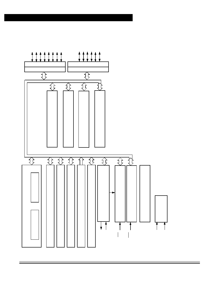
1.4 MCU Block Diagram
Figure 1-1
shows the structure of the MC68HC908RK2 MCU.
A
d
v
anc
e I
n
f
o
rm
at
i
o
n
M
C68
HC908RK
2
--
Rev
.
4.0
26
Ge
neral
Des
c
r
i
p
t
i
on
M
O
T
O
ROLA
Gene
r
a
l D
e
s
c
r
i
p
t
ion
Figure 1-1. MC68HC908RK2 MCU Block Diagram
SYSTEM INTEGRATION
MODULE
COMPUTER OPERATING PROPERLY
MODULE
SECURITY
MODULE
ARITHMETIC/LOGIC
UNIT (ALU)
CPU
REGISTERS
M68HC08 CPU
CONTROL AND STATUS REGISTERS -- 32 BYTES
USER FLASH -- 2031 BYTES
USER RAM -- 128 BYTES
MONITOR ROM -- 768 BYTES
USER FLASH VECTOR SPACE -- 14 BYTES
KEYBOARD/INTERRUPT
MODULE
POWER
INTERNAL BUS
V
DD
V
SS
PT
B
D
DRB
*
PIN CONTAINS INTEGRATED PULLUP RESISTOR
** HIGH CURRENT SINK PIN
PIN CONTAINS SOFTWARE SELECTABLE PULLUP RESISTOR
POWER-ON RESET
MODULE
LOW-VOLTAGE INHIBIT
MODULE
PTB2/TCH0
PTB3/TCLK
OSC1
OSC2
IRQ1
*
2-CHANNEL TIMER
MODULE
PT
A
DD
RA
PTA0**
PTA1/KBD1
**
PTA2/KBD2
**
PTA3/KBD3
**
PTA4/KBD4
**
PTA5/KBD5
**
PTA7**
PTA6/KBD6
**
PTB1
PTB0/MCLK
RST
*
PTB4/TCH1
PTB5
SOFTWARE SELECTABLE
INTERNAL OSCILLATOR
MODULE

General Description
Pin Assignments
MC68HC908RK2 -- Rev. 4.0
Advance Information
MOTOROLA
General Description
27
1.5 Pin Assignments
Figure 1-2
shows the pin assignments.
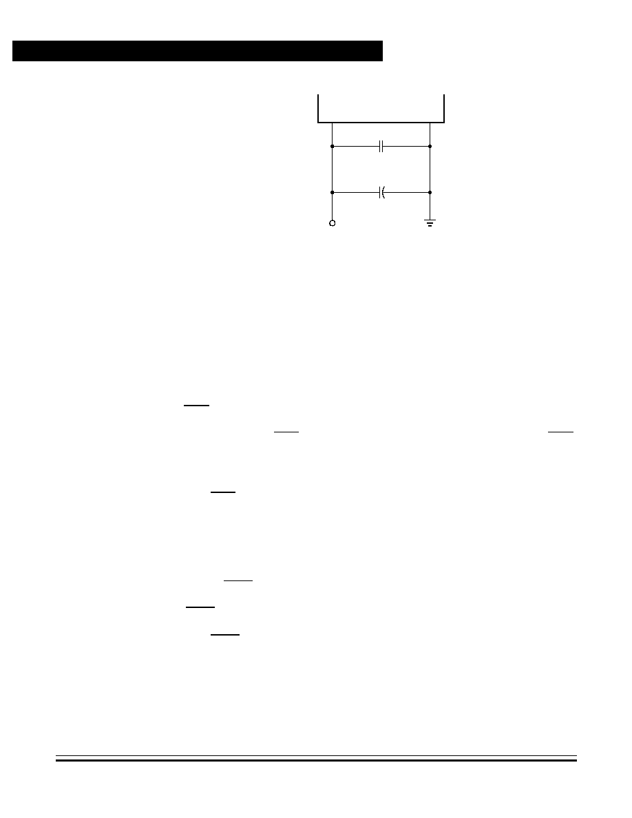
Figure 1-2. SSOP/SOIC Pin Assignments
1.5.1 Power Supply Pins (V
DD
and V
SS
)
V
DD
and V
SS
are the power supply and ground pins. The MCU operates
from a single power supply.
Fast signal transitions on MCU pins place high, short-duration current
demands on the power supply. To prevent noise problems, take special
care to provide power supply bypassing at the MCU as shown in
Figure 1-3
. Place the bypass capacitors as close to the MCU power pins
as possible. Use high-frequency-response ceramic capacitors for
C
Bypass
. C
Bulk
are optional bulk current bypass capacitors for use in
applications that require the port pins to source high current levels.
PTA0
PTB0/MCLK
PTB1
PTB2/TCH0
PTB4/TCH1
PTB5
PTB3/TCLK
OSC1
OSC2
V
SS
1
2
3
4
5
6
7
8
9
10
20
19
18
17
16
15
14
13
12
11
PTA1/KBD1
PTA2/KBD2
PTA3/KBD3
PTA4/KBD4
PTA5/KBD5
PTA6/KBD6
PTA7
RST
IRQ1
V
DD
Advance Information
MC68HC908RK2 -- Rev. 4.0
28
General Description
MOTOROLA
General Description
Figure 1-3. Power Supply Bypassing
1.5.2 Oscillator Pins (OSC1 and OSC2)
The OSC1
and
OSC2 pins are the connections to an external clock
source or crystal/ceramic resonator.
1.5.3 External Reset (RST)
A logic 0 on the RST pin forces the MCU to a known startup state. RST
is bidirectional, allowing a reset of the entire system. It is driven low when
any internal reset source is asserted.
The RST pin contains an internal pullup resistor.
For additional information, see
Section 6. System Integration Module
(SIM)
.
1.5.4 External Interrupt Pin (IRQ1)
IRQ1 is an asynchronous external interrupt pin.
The IRQ1 pin contains an internal pullup resistor.
MCU
V
DD
C
Bulk
V
SS
V
DD
+
Note: Component values shown represent typical applications.
C
Bypass
0.1
µ
F

General Description
Pin Assignments
MC68HC908RK2 -- Rev. 4.0
Advance Information
MOTOROLA
General Description
29
1.5.5 Port A Input/Output Pins (PTA7, PTA6/KBD6≠PTA1/KBD1, and PTA0)
Port A is an 8-bit special function port that shares its pins with the
keyboard interrupt.
Six port A pins (PTA6≠PTA1) can be programmed to serve as an
external interrupt. Once enabled, that pin will contain an internal pullup
resistor.
All port A pins are high-current sink pins.
1.5.6 Port B Input/Output Pins (PTB5, PTB4/TCH1, PTB3/TCLK, PTB2/TCH0,
PTB1, and PTB0/MCLK)
Port B is a 6-bit, general-purpose, bidirectional I/O port, with some of its
pins shared with the timer (TIM) module.

Advance Information
MC68HC908RK2 -- Rev. 4.0
30
General Description
MOTOROLA
General Description

MC68HC908RK2 -- Rev. 4.0
Advance Information
MOTOROLA
Memory Map
31
Advance Information -- MC68HC908RK2
Section 2. Memory Map
2.1 Contents
2.2
Introduction . . . . . . . . . . . . . . . . . . . . . . . . . . . . . . . . . . . . . . . . 31
2.3
Input/Output Section . . . . . . . . . . . . . . . . . . . . . . . . . . . . . . . . . 33
2.4
Monitor ROM . . . . . . . . . . . . . . . . . . . . . . . . . . . . . . . . . . . . . .40
2.2 Introduction
The memory map, shown in
Figure 2-1
, includes:
∑
2031 bytes of user FLASH memory
∑
128 bytes of random-access memory (RAM)
∑
14 bytes of user-defined vectors in FLASH memory
∑
768 bytes of monitor read-only memory (ROM)
These definitions apply to the memory map representation of reserved
and unimplemented locations:
∑
Reserved -- Accessing a reserved location can have
unpredictable effects on MCU operation.
∑
Unimplemented -- Accessing an unimplemented location causes
an illegal address reset.
Advance Information
MC68HC908RK2 -- Rev. 4.0
32
Memory Map
MOTOROLA
Memory Map
$0000
$003F
I/O REGISTERS (28 BYTES)
$0040
$007F
UNIMPLEMENTED (64 BYTES)
$0080
$00FF
RAM (128 Bytes)
$0100
$77FF
UNIMPLEMENTED (30,464 BYTES)
$7800
$7FEE
FLASH MEMORY (2031 BYTES)
$7FEF
OPTIONAL FACTORY DETERMINED ICG TRIM VALUE
(1)
$7FF0
$EFFF
UNIMPLEMENTED (28,688 BYTES)
$F000
$F2EF
MONITOR ROM (752 BYTES)
$F2F0
$FDFF
UNIMPLEMENTED (2832 BYTES)
$FE00
SIM BREAK STATUS REGISTER (SBSR)
$FE01
SIM RESET STATUS REGISTER (SRSR)
$FE02
SIM BREAK FLAG CONTROL REGISTER (SBFCR)
$FE03
$FE06
RESERVED (4 BYTES)
$FE07
UNIMPLEMENTED (1 BYTE)
$FE08
FLASH CONTROL REGISTER (FLCR)
$FE09
RESERVED (1 BYTE)
$FE0A
$FE0B
UNIMPLEMENTED (2 BYTES)
$FE0C
BREAK ADDRESS REGISTER HIGH (BRKH)
$FE0D
BREAK ADDRESS REGISTER LOW (BRKL)
1. Address $7FEF is reserved for an optional factory-determined ICG
trim value. Consult with a local Motorola representative for more
information and availability of this option.
Figure 2-1. Memory Map
Memory Map
Input/Output Section
MC68HC908RK2 -- Rev. 4.0
Advance Information
MOTOROLA
Memory Map
33
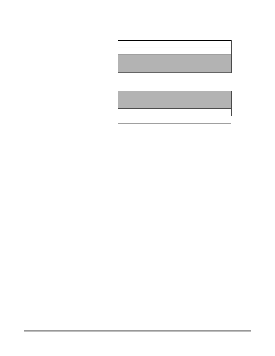
2.3 Input/Output Section
Addresses $0000≠$003F, shown in
Figure 2-2
, contain most of the
control, status, and data registers. Additional I/O registers have these
addresses:
∑
$FE00 -- SIM break status register, SBSR
∑
$FE01 -- SIM reset status register, SRSR
∑
$FE02 -- SIM break flag control register, BFCR
∑
$FE08 -- FLASH control register, FLCR
∑
$FE0C -- BREAK address register high, BRKH
∑
$FE0D -- BREAK address register low, BRKL
∑
$FE0E -- BREAK status and control register, BSCR
∑
$FE0F -- LVI status register, LVISR
∑
$FFF0 -- FLASH block protection register, FLBPR
∑
$FFFF -- COP control register, COPCTL
$FE0E
BREAK STATUS AND CONTROL REGISTER (BSCR)
$FE0F
LVI STATUS REGISTER (LVISR)
$FE10
$FEEF
UNIMPLEMENTED (222 BYTES)
$FEF0
$FEFF
MONITOR ROM (16 BYTES)
$FF00
$FFEF
UNIMPLEMENTED (240 BYTES)
$FFF0
FLASH BLOCK PROTECT REGISTER (FLBPR)
$FFF1
RESERVED (1 BYTE)
$FFF2
$FFFF
FLASH VECTORS
(14 Bytes)
Figure 2-1. Memory Map (Continued)
Advance Information
MC68HC908RK2 -- Rev. 4.0
34
Memory Map
MOTOROLA
Memory Map
Addr.
Register Name
Bit 7
6
5
4
3
2
1
Bit 0
$0000
Port A Data Register
(PTA)
See page 175.
Read:
PTA7
PTA6
PTA5
PTA4
PTA3
PTA2
PTA1
PTA0
Write:
Reset:
Unaffected by reset
$0001
Port B Data Register
(PTB)
See page 178.
Read:
PTB5
PTB4
PTB3
PTB2
PTB1
PTB0
Write:
Reset:
Unaffected by reset
$0002
Unimplemented
$0003
Unimplemented
$0004
Data Direction Register A
(DDRA)
See page 176.
Read:
DDRA7
DDRA6
DDRA5
DDRA4
DDRA3
DDRA2
DDRA1
DDRA0
Write:
Reset:
0
0
0
0
0
0
0
0
$0005
Data Direction Register B
(DDRB)
See page 179.
Read:
MCLKEN
0
DDRB5
DDRB4
DDRB3
DDRB2
DDRB1
DDRB0
Write:
Reset:
0
0
0
0
0
0
0
0
$0006
Unimplemented
$0019
Unimplemented
$001A
IRQ and Keyboard Status
and Control Register
(INTKBSCR)
See page 191.
Read:
IRQ1F
0
IMASKI
MODEI
KEYF
0
IMASKK
MODEK
Write:
R
ACKI
R
ACKK
Reset:
0
0
0
0
0
0
0
0
$001B
Keyboard Interrupt Enable
Register (INTKBIER)
See page 193.
Read:
0
KBIE6
KBIE5
KBIE4
KBIE3
KBIE2
KBIE1
0
Write:
Reset:
0
0
0
0
0
0
0
0
= Unimplemented
R
= Reserved U = Unaffected X = Indeterminate
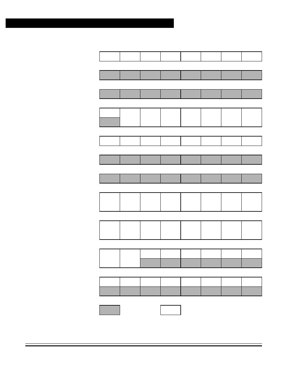
Figure 2-2. Control, Status, and Data Registers (Sheet 1 of 6)
Memory Map
Input/Output Section
MC68HC908RK2 -- Rev. 4.0
Advance Information
MOTOROLA
Memory Map
35
$001C
Unimplemented
$001E
Unimplemented
$001F
Configuration Register
(CONFIG)
See page 146.
Read:
EXTSLOW LVISTOP
LVIRST
LVIPWR
COPRS
SSREC
STOP
COPD
Write:
Reset:
0
0
1
1
0
0
0
0
$0020
Timer Status and Control
Register (TSC)
See page 208.
Read:
TOF
TOIE
TSTOP
0
0
PS2
PS1
PS0
Write:
0
TRST
Reset:
0
0
1
0
0
0
0
0
$0021
Timer Counter Register
High (TCNTH)
See page 210.
Read:
Bit 15
14
13
12
11
10
9
Bit 8
Write:
Reset:
0
0
0
0
0
0
0
0
$0022
Timer Counter Register
Low (TCNTL)
See page 210.
Read:
Bit 7
6
5
4
3
2
1
Bit 0
Write:
Reset:
0
0
0
0
0
0
0
0
$0023
Timer Counter Modulo
Register High (TMODH)
See page 211.
Read:
Bit 15
14
13
12
11
10
9
Bit 8
Write:
Reset:
1
1
1
1
1
1
1
1
$0024
Timer Counter Modulo
Register Low (TMODL)
See page 211.
Read:
Bit 7
6
5
4
3
2
1
Bit 0
Write:
Reset:
1
1
1
1
1
1
1
1
$0025
Timer Channel 0 Status
and Control Register
(TSC0)
See page 212.
Read:
CH0F
CH0IE
MS0B
MS0A
ELS0B
ELS0A
TOV0
CH0MAX
Write:
0
Reset:
0
0
0
0
0
0
0
0
Addr.
Register Name
Bit 7
6
5
4
3
2
1
Bit 0
= Unimplemented
R
= Reserved U = Unaffected X = Indeterminate
Figure 2-2. Control, Status, and Data Registers (Sheet 2 of 6)
Advance Information
MC68HC908RK2 -- Rev. 4.0
36
Memory Map
MOTOROLA
Memory Map
$0026
Timer Channel 0 Register
High (TCH0H)
See page 216.
Read:
Bit 15
14
13
12
11
10
9
Bit 8
Write:
Reset:
Indeterminate after reset
$0027
Timer Channel 0 Register
Low (TCH0L)
See page 216.
Read:
Bit 7
6
5
4
3
2
1
Bit 0
Write:
Reset:
Indeterminate after reset
$0028
Timer Channel 1 Status
and Control Register
(TSC1)
See page 212.
Read:
CH1F
CH1IE
0
MS1A
ELS1B
ELS1A
TOV1
CH1MAX
Write:
0
Reset:
0
0
0
0
0
0
0
0
$0029
Timer Channel 1 Register
High (TCH1H))
See page 216.
Read:
Bit 15
14
13
12
11
10
9
Bit 8
Write:
Reset:
Indeterminate after reset
$002A
Timer Channel 1 Register
Low (TCH1L))
See page 216.
Read:
Bit 7
6
5
4
3
2
1
Bit 0
Write:
Reset:
Indeterminate after reset
$002B
Unimplemented
$0035
Unimplemented
$0036
Internal Clock Generator
Control Register
(ICGCR)
See page 139.
Read:
CMIE
CMF
CMON
CS
ICGON
ICGS
ECGON
ECGS
Write:
Reset:
0
0
0
0
1
0
0
0
$0037
Internal Clock Generator
Multiplier Register
(ICGMR)
See page 141.
Read:
R
N6
N5
N4
N3
N2
N1
N0
Write:
Reset:
0
0
0
1
0
1
0
1
Addr.
Register Name
Bit 7
6
5
4
3
2
1
Bit 0
= Unimplemented
R
= Reserved U = Unaffected X = Indeterminate
Figure 2-2. Control, Status, and Data Registers (Sheet 3 of 6)
Memory Map
Input/Output Section
MC68HC908RK2 -- Rev. 4.0
Advance Information
MOTOROLA
Memory Map
37
$0038
Internal Clock Generator
Trim Register (ICGTR)
See page 142.
Read:
TRIM7
TRIM6
TRIM5
TRIM4
TRIM3
TRIM2
TRIM1
TRIM0
Write:
Reset:
1
0
0
0
0
0
0
0
$0039
ICG DCO Divider
Control Register
(ICGDVR)
See page 143.
Read:
R
R
R
R
DDIV3
DDIV2
DDIV1
DDIV0
Write:
Reset:
0
0
0
0
U
U
U
U
$003A
ICG DCO Stage Register
(ICGDSR)
See page 144.
Read:
DSTG7
DSTG6
DSTG5
DSTG4
DSTG3
DSTG2
DSTG1
DSTG0
Write:
Reset:
Unaffected by reset
$003B
Reserved
R
R
R
R
R
R
R
R
$003C
Unimplemented
$003F
Unimplemented
$FE00
SIM Break Status Register
(SBSR)
See page 97.
Read:
R
R
R
R
R
R
SBSW
R
Write:
See Note
Reset:
0
Note: Writing a logic 0 clears SBSW
$FE01
SIM Reset Status Register
(SRSR)
See page 98.
Read:
POR
PIN
COP
ILOP
ILAD
0
LVI
0
Write:
POR:
1
X
X
X
X
X
X
X
$FE02
SIM Break Flag Control
Register (SBFCR)
See page 99.
Read:
BCFE
R
R
R
R
R
R
R
Write:
Reset:
0
0
0
0
0
0
0
0
$FE03
Reserved
R
R
R
R
R
R
R
R
Addr.
Register Name
Bit 7
6
5
4
3
2
1
Bit 0
= Unimplemented
R
= Reserved U = Unaffected X = Indeterminate
Figure 2-2. Control, Status, and Data Registers (Sheet 4 of 6)
Advance Information
MC68HC908RK2 -- Rev. 4.0
38
Memory Map
MOTOROLA
Memory Map
$FE04
Reserved
R
R
R
R
R
R
R
R
$FE05
Unimplemented
$FE07
Unimplemented
$FE08
FLASH 2TS Control
Register (FLCR)
See page 45.
Read:
0
FDIV0
BLK1
BLK0
HVEN
MARGIN
ERASE
PGM
Write:
Reset:
0
0
0
0
0
0
0
0
$FE09
Reserved
R
R
R
R
R
R
R
R
$FE0A
Unimplemented
$FE0B
Unimplemented
$FE0C
Break Address Register
High (BRKH)
See page 106.
Read:
Bit 15
14
13
12
11
10
9
Bit 8
Write:
Reset:
0
0
0
0
0
0
0
0
$FE0D
Break Address Register
Low (BRKL)
See page 106.
Read:
Bit 7
6
5
4
3
2
1
Bit 0
Write:
Reset:
0
0
0
0
0
0
0
0
$FE0E
Break Status and Control
Register (BSCR)
See page 105.
Read:
BRKE
BRKA
0
0
0
0
0
0
Write:
Reset:
0
0
0
0
0
0
0
0
$FE0F
LVI Status Register
(LVISR)
See page 170.
Read: LVIOUT
0
LOWV
0
0
0
0
0
Write:
Reset:
0
0
0
0
0
0
0
0
Addr.
Register Name
Bit 7
6
5
4
3
2
1
Bit 0
= Unimplemented
R
= Reserved U = Unaffected X = Indeterminate
Figure 2-2. Control, Status, and Data Registers (Sheet 5 of 6)
Memory Map
Input/Output Section
MC68HC908RK2 -- Rev. 4.0
Advance Information
MOTOROLA
Memory Map
39
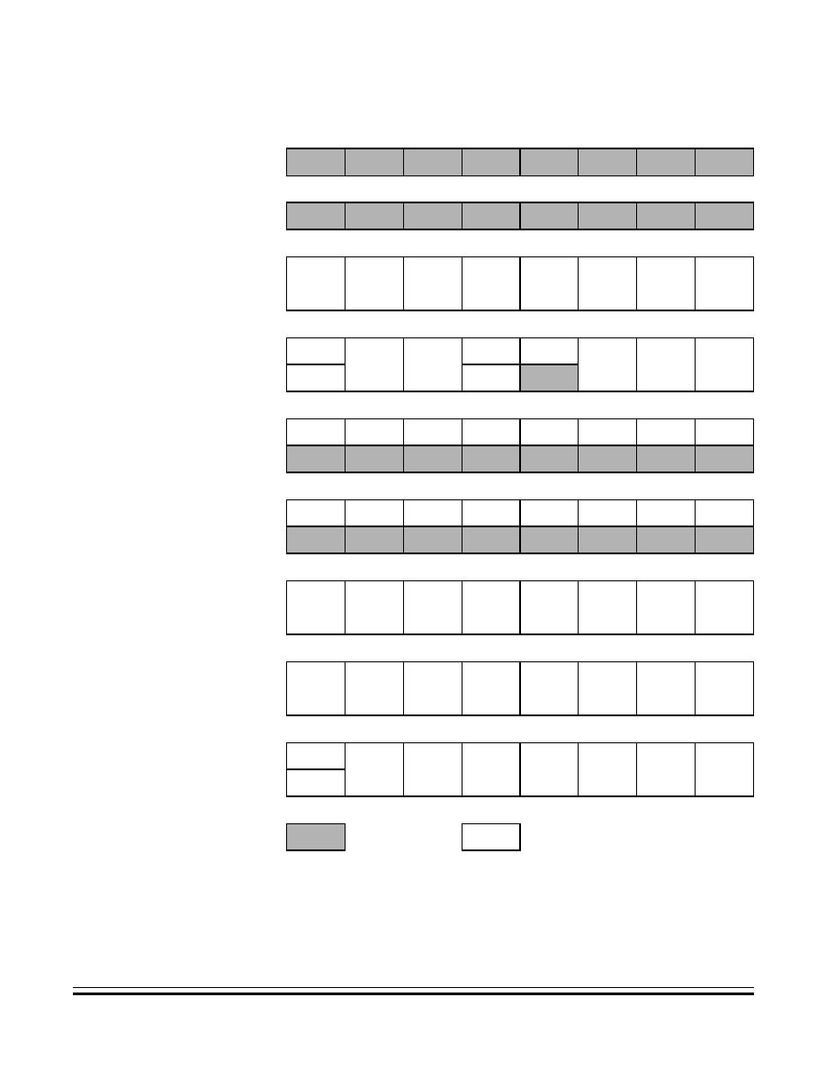
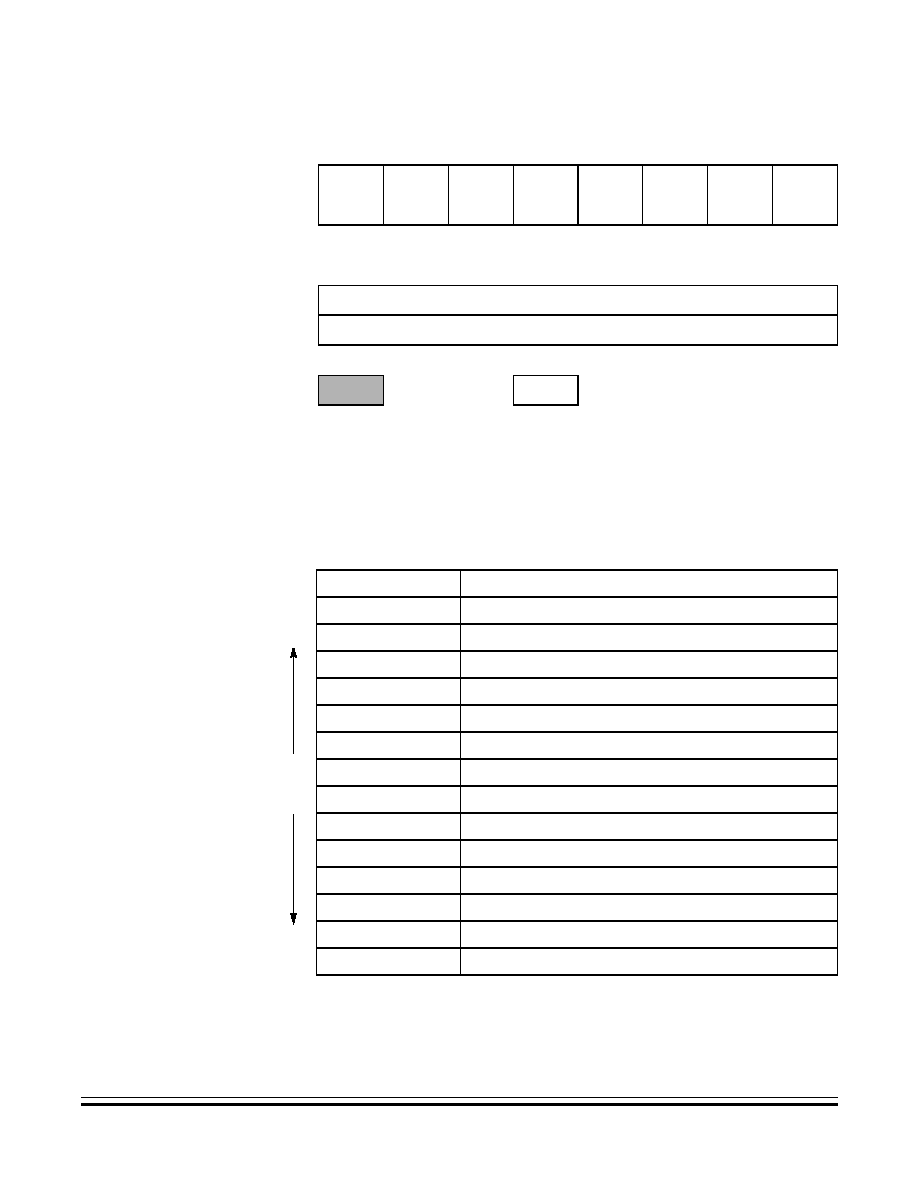
Table 2-1
is a list of vector locations.
$FFF0
FLASH Block Protect
Register (FLBPR)
See page 52.
Read:
R
R
R
R
BPR3
BPR2
BPR1
BPR0
Write:
Reset:
Unaffected by reset
Non-volatile FLASH register
$FFFF
COP Control Register
(COPCTL)
See page 165.
Read:
Low byte of reset vector
Write:
Writing clears COP counter (any value)
Reset:
Unaffected by reset
Addr.
Register Name
Bit 7
6
5
4
3
2
1
Bit 0
= Unimplemented
R
= Reserved U = Unaffected X = Indeterminate
Figure 2-2. Control, Status, and Data Registers (Sheet 6 of 6)
Table 2-1. Vector Locations
Address
Vector
Lo
w
$FFF2
ICG vector (high)
$FFF3
ICG vector (low)
Pr
i
o
r
i
ty
$FFF4
TIM overflow vector (high)
$FFF5
TIM overflow vector (low)
$FFF6
TIM channel 1 vector (high)
$FFF7
TIM channel 1 vector (low)
$FFF8
TIM channel 0 vector (high)
$FFF9
TIM channel 0 vector (low)
$FFFA
IRQ1/keyboard vector (high)
$FFFB
IRQ1/keyboard vector (low)
$FFFC
SWI vector (high)
$FFFD
SWI vector (low)
Hi
g
h
$FFFE
Reset vector (high)
$FFFF
Reset vector (low)

Advance Information
MC68HC908RK2 -- Rev. 4.0
40
Memory Map
MOTOROLA
Memory Map
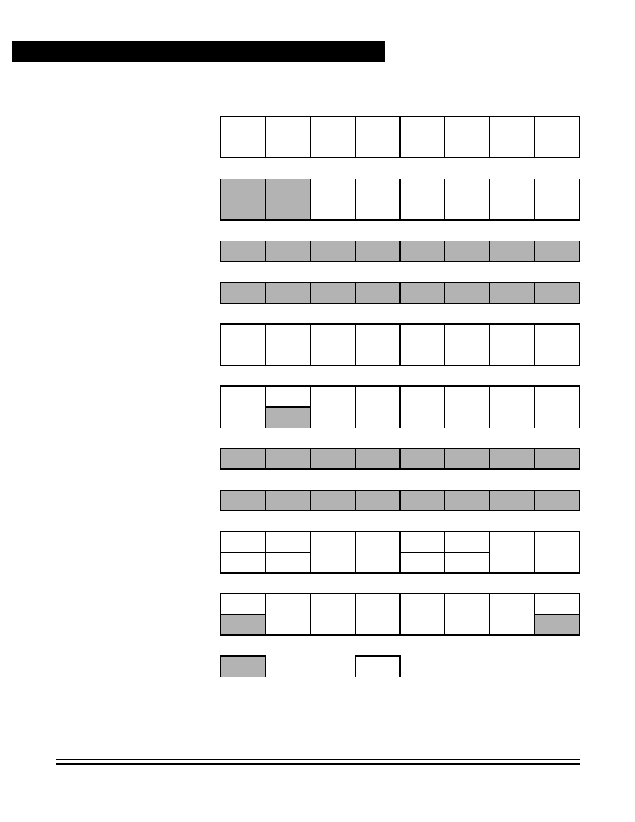
2.4 Monitor ROM
The 768 bytes at addresses $F000≠F2EF and $FEF0≠$FEFF are
utilized by the monitor ROM.
The address range $F000≠F2EF is reserved for the monitor code
functions, FLASH memory programming, and erase algorithms.
The address range $FEF0≠$FEFF holds reserved ROM addresses that
contain the monitor code reset vectors.

MC68HC908RK2 -- Rev. 4.0
Advance Information
MOTOROLA
Random-Access Memory (RAM)
41
Advance Information -- MC68HC908RK2
Section 3. Random-Access Memory (RAM)
3.1 Contents
3.2
Introduction . . . . . . . . . . . . . . . . . . . . . . . . . . . . . . . . . . . . . . . . 41
3.3
Functional Description . . . . . . . . . . . . . . . . . . . . . . . . . . . . . . . 41
3.2 Introduction
This section describes the 128 bytes of random-access memory (RAM).
3.3 Functional Description
Addresses $0080≠$00FF are RAM locations. The location of the stack
RAM is programmable.
NOTE:
For correct operation, the stack pointer must point only to RAM
locations.
Before processing an interrupt, the CPU uses five bytes of the stack to
save the contents of the CPU registers.
NOTE:
For M68HC05, M6805, and M146805 compatibility, the H register is not
stacked.
During a subroutine call, the CPU uses two bytes of the stack to store
the return address. The stack pointer decrements during pushes and
increments during pulls.
NOTE:
Be careful when using nested subroutines. The CPU could overwrite
data in the RAM during a subroutine or during the interrupt stacking
operation.

Advance Information
MC68HC908RK2 -- Rev. 4.0
42
Random-Access Memory (RAM)
MOTOROLA
Random-Access Memory (RAM)

MC68HC908RK2 -- Rev. 4.0
Advance Information
MOTOROLA
FLASH 2TS Memory
43
Advance Information -- MC68HC908RK2
Section 4. FLASH 2TS Memory
4.1 Contents
4.2
Introduction . . . . . . . . . . . . . . . . . . . . . . . . . . . . . . . . . . . . . . . . 43
4.3
Functional Description . . . . . . . . . . . . . . . . . . . . . . . . . . . . . . . 44
4.4
FLASH 2TS Control Register . . . . . . . . . . . . . . . . . . . . . . . . . . 45
4.5
FLASH 2TS Charge Pump Frequency Control. . . . . . . . . . . . . 47
4.6
FLASH 2TS Erase Operation . . . . . . . . . . . . . . . . . . . . . . . . . . 47
4.7
FLASH 2TS Program/Margin Read Operation . . . . . . . . . . . . . 48
4.8
FLASH 2TS Block Protection . . . . . . . . . . . . . . . . . . . . . . . . . . 51
4.9
FLASH 2TS Block Protect Register . . . . . . . . . . . . . . . . . . . . . 52
4.10
Embedded Program/Erase Routines . . . . . . . . . . . . . . . . . . . . 53
4.11
Embedded Function Descriptions. . . . . . . . . . . . . . . . . . . . . . . 54
4.11.1
RDVRRNG Routine . . . . . . . . . . . . . . . . . . . . . . . . . . . . . . . 54
4.11.2
PRGRNGE Routine . . . . . . . . . . . . . . . . . . . . . . . . . . . . . . . 55
4.11.3
ERARNGE Routine . . . . . . . . . . . . . . . . . . . . . . . . . . . . . . . 56
4.11.4
REDPROG Routine . . . . . . . . . . . . . . . . . . . . . . . . . . . . . . . 57
4.11.5
Example Routine Calls . . . . . . . . . . . . . . . . . . . . . . . . . . . . .58
4.12
Low-Power Modes . . . . . . . . . . . . . . . . . . . . . . . . . . . . . . . . . . 60
4.12.1
Wait Mode . . . . . . . . . . . . . . . . . . . . . . . . . . . . . . . . . . . . . .60
4.12.2
Stop Mode . . . . . . . . . . . . . . . . . . . . . . . . . . . . . . . . . . . . . .61
4.2 Introduction
This section describes the operation of the embedded FLASH 2TS
memory. This memory can be read, programmed, and erased from a
single external supply. The program and erase operations are enabled
through the use of an internal charge pump.

Advance Information
MC68HC908RK2 -- Rev. 4.0
44
FLASH 2TS Memory
MOTOROLA
FLASH 2TS Memory
4.3 Functional Description
The FLASH 2TS memory is appropriately named to describe its
2-transistor source-select bit cell. The FLASH 2TS memory is an array
of 2031 bytes with an additional 14 bytes of user vectors and one byte
for block protection. An erased bit reads as a logic 0 and a programmed
bit reads as a logic 1.
The address ranges for the user memory, control register, and vectors
are:
∑
$7800≠$7FEE, user space
∑
$7FEF, reserved -- optional ICG TRIM value, see
8.8.3 ICG Trim
Register
∑
$FFF0, block protect register
∑
$FE08, FLASH 2TS control register
∑
$FFF2≠$FFFF, these locations are reserved for user-defined
interrupt and reset vectors
This list is the row architecture for the user space array:
$7800≠$7807 (Row 0)
$7808≠$780F (Row 1)
$7810≠$7817 (Row 2)
$7818≠$781F (Row 3)
$7820≠$7827 (Row 4)
--------------------------
$7FE8≠$7FEF (Row 253)
Program and erase operations are facilitated through control bits in a
memory mapped register. Details for these operations appear later in
this section. Memory in the FLASH 2TS array is organized into pages
within rows. For the 2-Kbyte array on the MC68HC908RK2, the page
size is one byte. There are eight pages (or eight bytes) per row.
Programming operations are performed on a page basis, one byte at
time. Erase operations are performed on a block basis. The minimum

FLASH 2TS Memory
FLASH 2TS Control Register
MC68HC908RK2 -- Rev. 4.0
Advance Information
MOTOROLA
FLASH 2TS Memory
45
block size is one row of eight bytes. Refer to
Table 4-2
for additional
block size options.
NOTE:
Sometimes a program disturb condition, in which case an erased bit on
the row being programmed unintentionally becomes programmed,
occurs. The embedded smart programming algorithm implements a
margin read technique to avoid program disturb. The margin read step
of the smart programming algorithm is used to ensure programmed bits
are programmed to sufficient margin for data retention over the device's
lifetime. In the application code, perform an erase operation after eight
program operations (on the same row) to further avoid program disturb.
For availability of programming tools and more information, contact a
local Motorola representative.
NOTE:
A security feature prevents viewing of the FLASH 2TS contents.
(1)
4.4 FLASH 2TS Control Register
The FLASH 2TS control register (FLCR) controls program, erase, and
margin read operations.
FDIV0 -- Frequency Divide Control Bit
This read/write bit selects the factor by which the charge pump clock
is divided from the system clock. See
4.5 FLASH 2TS Charge Pump
Frequency Control
.
1. No security feature is absolutely secure. However, Motorola's strategy is to make reading or
copying the FLASH 2TS difficult for unauthorized users.
Address:
$FE08
Bit 7
6
5
4
3
2
1
Bit 0
Read:
0
FDIV0
BLK1
BLK0
HVEN
MARGIN
ERASE
PGM
Write:
Reset:
0
0
0
0
0
0
0
0
= Unimplemented
Figure 4-1. FLASH 2TS Control Register (FLCR)

Advance Information
MC68HC908RK2 -- Rev. 4.0
46
FLASH 2TS Memory
MOTOROLA
FLASH 2TS Memory
BLK1 -- Block Erase Control Bit
This read/write bit together with BLK0 allows erasing of blocks of
varying size. See
4.6 FLASH 2TS Erase Operation
for a description
of available block sizes.
BLK0 -- Block Erase Control Bit
This read/write bit together with BLK1 allows erasing of blocks of
varying size. See
4.6 FLASH 2TS Erase Operation
for a description
of available block sizes.
HVEN -- High-Voltage Enable Bit
This read/write bit enables the charge pump to drive high voltages for
program and erase operations in the array. HVEN can be set only if
either PGM = 1 or ERASE = 1 and the proper sequence for smart
programming or erase is followed.
1 = High voltage enabled to array and charge pump on
0 = High voltage disabled to array and charge pump off
MARGIN -- Margin Read Control Bit
This read/write bit configures the memory for margin read operation.
MARGIN cannot be set if the HVEN = 1. MARGIN will automatically
return to unset (0) if asserted when HVEN = 1.
1 = Margin read operation selected
0 = Margin read operation unselected
ERASE -- Erase Control Bit
This read/write bit configures the memory for erase operation.
ERASE is interlocked with the PGM bit such that both bits cannot be
set at the same time.
1 = Erase operation selected
0 = Erase operation unselected
PGM -- Program Control Bit
This read/write bit configures the memory for program operation.
PGM is interlocked with the ERASE bit such that both bits cannot be
set at the same time.
1 = Program operation selected
0 = Program operation unselected

FLASH 2TS Memory
FLASH 2TS Charge Pump Frequency Control
MC68HC908RK2 -- Rev. 4.0
Advance Information
MOTOROLA
FLASH 2TS Memory
47
4.5 FLASH 2TS Charge Pump Frequency Control
The internal charge pump, required for program, margin read, and erase
operations, is designed to operate most efficiently with a 2-MHz clock.
The charge pump clock is derived from the bus clock.
Table 4-1
shows
how the FDIV bits are used to select a charge pump frequency based on
the bus clock frequency. Program, margin read, and erase operations
cannot be performed if the bus clock frequency is below 2 MHz.
NOTE:
The charge pump is optimized for 2-MHz operation.
4.6 FLASH 2TS Erase Operation
Use this step-by-step procedure to erase a block of FLASH 2TS
memory. Refer to
16.12 Memory Characteristics
for a detailed
description of the times used in this algorithm.
1. Set the ERASE, BLK0, BLK1, and FDIV0 bits in the FLASH 2TS
control register. Refer to
Table 4-1
for FDIV settings and to
Table 4-2
for block sizes.
2. Ensure target portion of array is unprotected by reading the block
protect register at address $FFF0. Refer to
4.8 FLASH 2TS Block
Protection
and
4.9 FLASH 2TS Block Protect Register
for more
information.
3. Write to any FLASH 2TS address with any data within the block
address range desired.
4. Set the HVEN bit.
5. Wait for a time, t
Erase
.
6. Clear the HVEN bit.
Table 4-1. Charge Pump Clock Frequency
FDIV0
Pump Clock Frequency
0
Bus frequency
˜
1
1
Bus frequency
˜
2
Advance Information
MC68HC908RK2 -- Rev. 4.0
48
FLASH 2TS Memory
MOTOROLA
FLASH 2TS Memory
7. Wait for a time, t
Kill
, for the high voltages to dissipate.
8. Clear the ERASE bit.
9. After a time, t
HVD
, the memory can be accessed in read mode
again.
NOTE:
While these operations must be performed in the order shown, other
unrelated operations may occur between the steps.
Table 4-2
shows the various block sizes which can be erased in one
erase operation.
In step 3 of the erase operation, the cared addresses are latched and
used to determine the location of the block to be erased. For instance,
with BLK0 = BLK1 = 0, writing to any FLASH 2TS address in the range
$7800 to $78F0 will enable the erase of all FLASH memory.
4.7 FLASH 2TS Program/Margin Read Operation
NOTE:
After a total of eight program operations have been applied to a row, the
row must be erased before further programming to avoid program
disturb. An erased byte will read $00.
The FLASH 2TS memory is programmed on a page basis. A page
consists of one byte. The smart programming algorithm (
Figure 4-2
) is
recommended to program every page in the FLASH 2TS memory.
Table 4-2. Erase Block Sizes
BLK1
BLK0
Block Size, Addresses Cared
0
0
Full array: 2 Kbytes
0
1
One-half array: 1 Kbytes
1
0
Eight rows: 64 bytes
1
1
Single row: 8 bytes

FLASH 2TS Memory
FLASH 2TS Program/Margin Read Operation
MC68HC908RK2 -- Rev. 4.0
Advance Information
MOTOROLA
FLASH 2TS Memory
49
The embedded smart programming algorithm uses this step-by-step
sequence to program the data into the FLASH memory. The algorithm
optimizes the time required to program each page. Refer to
4.10
Embedded Program/Erase Routines
for information on utilizing
embedded routines.
1. Set the FDIV bits. These bits determine the charge pump
frequency.
2. Set PGM = 1. This configures the memory for program operation
and enables the latching of address and data for programming.
3. Read the FLASH 2TS block protect register (FLBPR).
4. Write data to the one byte being programmed.
5. Set HVEN = 1.
6. Wait for a time, t
Step
.
7. Set HVEN = 0.
8. Wait for a time, t
HVTV
.
9. Set MARGIN = 1.
10. Wait for a time, t
VTP
.
11. Set PGM = 0.
12. Wait for a time, t
HVD
.
13. Read back data in margin read mode. This read operation is
stretched by eight cycles.
14. Clear the MARGIN bit. If the margin read data is identical to
write data, the program operation is complete; otherwise, jump to
step 2.
NOTE:
While these operations must be performed in the order shown, other
unrelated operations may occur between the steps.
The smart programming algorithm guarantees the minimum possible
program time.
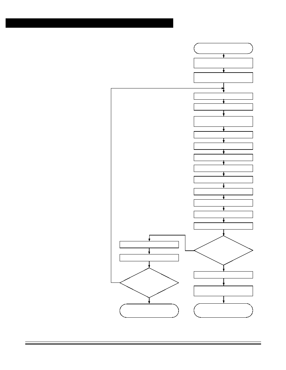
Advance Information
MC68HC908RK2 -- Rev. 4.0
50
FLASH 2TS Memory
MOTOROLA
FLASH 2TS Memory
Figure 4-2. Smart Programming Algorithm Flowchart
PROGRAM FLASH 2TS
INITIALIZE ATTEMPT COUNTER
SET PGM BIT AND FDIV BITS
WAIT T
HVTV
WAIT t
VTP
SET HVEN BIT
CLEAR PGM BIT
SET MARGIN BIT
WAIT t
HVD
INCREMENT ATTEMPT COUNTER
Y
N
TO 0
Y
N
PROGRAMMING OPERATION
FAILED
PROGRAMMING OPERATION
COMPLETE
WRITE DATA TO
SELECTED PAGE
WAIT t
STEP
CLEAR HVEN BIT
MARGIN READ PAGE OF DATA
CLEAR MARGIN BIT
MARGIN READ DATA
EQUAL TO
WRITE DATA?
READ FLASH BLOCK PROTECT REG.
Page Program/Margin Read Procedure
Note: This page program algorithm
assumes the page/s to be programmed
are initially erased.
Note: This algorithm is mandatory for
programming the FLASH 2TS.
SET INTERRUPT MASK:
CLEAR MARGIN BIT
CLEAR INTERRUPT MASK:
SEI INSTRUCTION
CLI INSTRUCTION
ATTEMPT COUNT
EQUAL TO
fls
Pulses
?

FLASH 2TS Memory
FLASH 2TS Block Protection
MC68HC908RK2 -- Rev. 4.0
Advance Information
MOTOROLA
FLASH 2TS Memory
51
4.8 FLASH 2TS Block Protection
NOTE:
In performing a program or erase operation, the FLASH 2TS block
protect register must be read after setting the PGM or ERASE bit and
before asserting the HVEN bit.
Due to the ability of the on-board charge pump to erase and program the
FLASH 2TS memory in the target application, provision is made for
protecting blocks of memory from unintentional erase or program
operations due to system malfunction. This protection is implemented by
a reserved location in the memory for block protect information. This
block protect register must be read before setting HVEN = 1. When the
block protect register is read, its contents are latched by the FLASH 2TS
control logic. If the address range for an erase or program operation
includes a protected block, the PGM or ERASE bit is cleared which
prevents the HVEN bit in the FLASH 2TS control register from being set
such that no high-voltage operation is allowed in the array.
When the block protect register is erased (all 0s), the entire memory is
accessible for program and erase. When bits within the register are
programmed, they lock blocks of memory address ranges as shown in
4.9 FLASH 2TS Block Protect Register
. The block protect register
itself can be erased or programmed only with an external voltage V
HI
present on the IRQ1 pin. The presence of V
HI
on the IRQ1 pin also
allows entry into monitor mode out of reset. Therefore, the ability to
change the block protect register is voltage-level dependent and can
occur in either user or monitor modes.
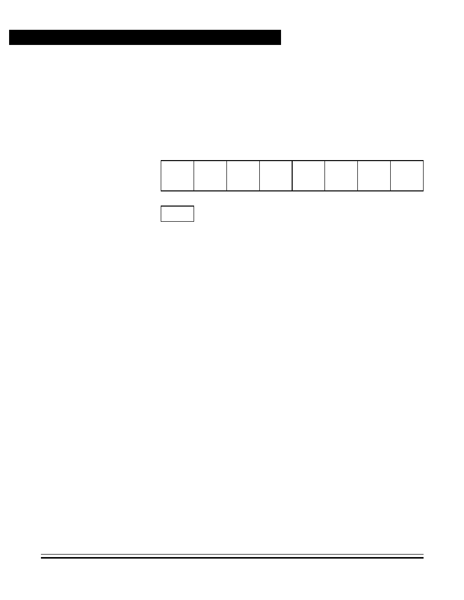
Advance Information
MC68HC908RK2 -- Rev. 4.0
52
FLASH 2TS Memory
MOTOROLA
FLASH 2TS Memory
4.9 FLASH 2TS Block Protect Register
The block protect register (FLBPR) is implemented as a byte within the
FLASH 2TS memory. Each bit, when programmed, protects a range of
addresses in the FLASH 2TS.
BPR3 -- Block Protect Register Bit 3
This bit protects the memory contents in the address ranges
$7A00≠$7FEF and $FFF0≠$FFFF.
1 = Address range protected from erase or program
0 = Address range open to erase or program
BPR2 -- Block Protect Register Bit 2
This bit protects the memory contents in the address ranges
$7900≠$7FEF and $FFF0≠$FFFF.
1 = Address range protected from erase or program
0 = Address range open to erase or program
BPR1 -- Block Protect Register Bit 1
This bit protects the memory contents in the address ranges
$7880≠$7FEF and $FFF0≠$FFFF.
1 = Address range protected from erase or program
0 = Address range open to erase or program
BPR0 -- Block Protect Register Bit 0
This bit protects the FLASH memory contents in the address ranges
$7800≠$7FEF and $FFF0≠$FFFF.
1 = Address range protected from erase or program
0 = Address range open to erase or program
Address:
$FFF0
Bit 7
6
5
4
3
2
1
Bit 0
Read:
R
R
R
R
BPR3
BPR2
BPR1
BPR0
Write:
Reset:
Unaffected by reset
R
= Reserved
Figure 4-3. FLASH 2TS Block Protect Register (FLBPR)
FLASH 2TS Memory
Embedded Program/Erase Routines
MC68HC908RK2 -- Rev. 4.0
Advance Information
MOTOROLA
FLASH 2TS Memory
53
By programming the block protect bits, a portion of the memory will be
locked so that no further erase or program operations may be
performed. Programming more than one bit at a time is redundant. If
both bit 1 and bit 2 are set, for instance, the FLASH address ranges
between $7880≠$FFFF are locked. If all bits are erased, then all of the
memory is available for erase and program.
The presence of a voltage V
HI
on the IRQ1 pin will bypass the block
protection so that all of memory, including the block protect register, can
be programmed or erased.
4.10 Embedded Program/Erase Routines
The MC68HC908RK2 monitor ROM contains numerous routines for
programming and erasing the FLASH memory. These embedded
routines are intended to assist the programmer with modifying the
FLASH memory array. These routines will implement the smart
programming algorithm as defined in
Figure 4-2
. The functions are listed
in
Table 4-3
.
The functions shown in
Table 4-3
accept data through the CPU registers
and global variables in RAM.
Table 4-4
shows the RAM locations that
are used for passing parameters.
Table 4-3. Embedded FLASH Routines
Function Description
Call
JSR to Address
(1)
1. ROMSTRT is defined as the starting address of the monitor ROM in the memory map. This
is address $F000.
Read/verify a range
RDVRRNG
ROMSTRT + 0
Program range of FLASH
PRGRNGE
ROMSTRT + 3
Erase range of FLASH
ERARNGE
ROMSTRT + 6
Redundant program FLASH
REDPROG
ROMSTRT + 9
Advance Information
MC68HC908RK2 -- Rev. 4.0
54
FLASH 2TS Memory
MOTOROLA
FLASH 2TS Memory
4.11 Embedded Function Descriptions
This subsection describes the embedded functions.
4.11.1 RDVRRNG Routine
Name:
RDVRRNG
Purpose:
Read and/or verify a range of FLASH memory
Entry conditions:
H:X
Contains the first address of the range
LADDR
Contains the last address of the range
DATA
Contains the data to compare the read data against for
read/verify to RAM only (length is user determined)
ACC
Non-zero for read/verify to RAM, 0 for output to PA0
Exit conditions:
C bit
Set if good compare for read/verify to RAM only
ACC
Contains checksum
DATA
Contains read FLASH data for read/verify to RAM only
Table 4-4. Embedded FLASH Routine Global Variables
Variable Location
Variable Address
(1)
CTRLBYT
RAMSTART + 8
CPUSPD
RAMSTART + 9
LADDR
RAMSTART + 10
BUMPS
RAMSTART + 12
DERASE
RAMSTART + 13
DATA
RAMSTART + 15
1. RAMSTART is defined as the starting address of the RAM in the memory map.
This is address $0080.

FLASH 2TS Memory
Embedded Function Descriptions
MC68HC908RK2 -- Rev. 4.0
Advance Information
MOTOROLA
FLASH 2TS Memory
55
Ready/verify
RAM optioin:
This subroutine both compares data passed in the DATA array to the
FLASH data and reads the data from FLASH into the DATA array. It also
calculates the checksum of the data.
Output to PA0
option:
This subroutine dumps the data from the range to PA0 in the same
format as monitor data. It also calculates the checksum of the data.
NOTE:
This serial dump does not circumvent security because the security
vectors must still be passed to make FLASH readable in monitor mode.
4.11.2 PRGRNGE Routine
Name:
PRGRNGE
Purpose:
Programs a range of addresses in FLASH memory
Entry conditions:
H:X
Contains the first address in the range
LADDR
Contains the last address in the range
DATA
Contains the data to be programmed (length is user
determined)
CPUSPD
Contains the bus frequency times 4 in MHz
BUMPS
Contains the maximum allowable number of programming
bumps to use
Exit conditions:
C bit
Set if successful program; cleared otherwise
I bit
Set, masking interrupts
This routine programs a range of FLASH defined by H:X and LADDR.
The range can be from one byte to as much RAM as can be allocated to
DATA. The smart programming algorithm defined in
4.7 FLASH 2TS
Program/Margin Read Operation
is used.
Advance Information
MC68HC908RK2 -- Rev. 4.0
56
FLASH 2TS Memory
MOTOROLA
FLASH 2TS Memory
4.11.3 ERARNGE Routine
Name:
ERARNGE
Purpose:
Erase a range of addresses in FLASH memory
Entry conditions:
H:X
Contains an address in the range to be erased; range size
specified by control byte
CTLBYTE Contains the erase block size in bits 5 and 6 (see
Table 4-5
)
DERASE
Contains the erase delay time in
µ
s/24
CPUSPD
CPU frequency times 4 in MHz
Exit conditions:
I bit
Set, masking interrupts.
This routine erases the block of FLASH defined by H:X and CTLBYTE.
The algorithm defined in
4.6 FLASH 2TS Erase Operation
is used.
Preserves the contents of H:X (address passed)
Table 4-5. CTLBYTE-Erase Block Size
Bit 6
Bit 5
Block Size
0
0
Full array
0
1
One half array
1
0
Eight rows: 64 pages
1
1
Single row: 8 pages

FLASH 2TS Memory
Embedded Function Descriptions
MC68HC908RK2 -- Rev. 4.0
Advance Information
MOTOROLA
FLASH 2TS Memory
57
4.11.4 REDPROG Routine
Name:
REDPROG
Purpose:
This routine will use a range of multiple rows in the FLASH array to
emulate increased write/erase cycling capability of one row.
Entry conditions:
H:X
Contains the address of the first row in the range. This
address must be the first address of a row (multiple of eight
bytes)
LADDR
Address of last row in the range; must be the first address
of a row (multiple of eight bytes)
DATA
Data to program in the row (bit 7 of DATA + 0 is used
internally and will be overwritten). Routine will always use
8 bytes starting at DATA
BUMPS
Contains the maximum allowable number of programming
bumps to use
CPUSPD
Contains the bus frequency times 4 in MHz
DERASE
Contains the erase delay time in
µ
s/24
Exit conditions:
C bit
Set if successful program; cleared otherwise
I bit
Set, masking interrupts
This routine uses a range of the FLASH array containing multiple rows
to emulate increased write/erase cycling capability for data storage. The
routine will write data to each row of the FLASH array (in the range
defined) upon subsequent calls. The number of rows is the difference
between the value in H:X and LADDR, divided by 8.
A row is the minimum range that can be programmed with the
REDPROG routine. All rows in the range will be programmed once
before any are programmed again. This approach is taken to ensure that
all rows reach the end of lifetime at approximately the same time.

Advance Information
MC68HC908RK2 -- Rev. 4.0
58
FLASH 2TS Memory
MOTOROLA
FLASH 2TS Memory
A special bit will be maintained by the routine, called a cycling bit, in each
row. This bit is used to ensure that the data is programmed to all the rows
defined in the range. This is the high bit of the first byte in each row. This
bit cannot be used to store user data. It will be modified by the
REDPROG routine. This is at bit 7 of the byte at address DATA+0.
To determine which row to program, the algorithm will step from the first
to the last row in a range looking for the first row whose cycling bit is
different from the first. If all rows contain the same cycling bit, then the
first row will be used.
The row whose cycling bit is different will be erased and the entire row
will be programmed with the given data, including a toggled version of
the cycling bit.
4.11.5 Example Routine Calls
This code is for illustrative purposes only and does not represent valid
syntax for any particular assembler.
RAM EQU
$80
RDVRRNG
EQU
$F000
PRGRNGE
EQU
$F003
ERANRGE
EQU
$F006
REDPROG EQU
$F009
;*************************************************************
RAM Definitions for Subroutines
;**************************************************************
ORG RAM+8
CTRLBYT
RMB
1
CPUSPD
RMB
1
LADDR
RMB 2
BUMPS
RMB 1
DERASE
RMB
2
;Allocation of "DATA" space is dependent on the device and
;application

FLASH 2TS Memory
Embedded Function Descriptions
MC68HC908RK2 -- Rev. 4.0
Advance Information
MOTOROLA
FLASH 2TS Memory
59
DATA
RMB 8
;*************************************************************
; CALLING EXAMPLE FOR READ/VERIFY A RANGE (RDVRRNG)
;**************************************************************
LDA
#$FF
;TARGET IS RAM
LDHX #$7807
;END AFTER FIRST ROW
STHX LADDR
LDHX #$7800
;START AT FIRST ROW
JSR RDVRRNG
;DATA WILL CONTAIN FLASH INFO
;*************************************************************
; CALLING EXAMPLE FOR ERASE A RANGE (ERARNGE)
;**************************************************************
MOV
#$08,CPUSPD ;Load Bus frequency in MHz * 4
MOV
#$60,CTRLBYT
;Bits 5&6 hold the block size to erase
;00 Full Array
;20 One-Half Array
;40 Eight Rows
;60 Singe Row
;Remember a Row is 1 byte
;Set erase time in uS/24, number in
;decimal
LDHX
#100000/24
STHX
DERASE
LDHX
#$7800
;Address in the range to erase
JSR
ERARNGE
;Call through jump table
;************************************************************;
; CALLING EXAMPLE FOR PROGRAM A RANGE (PRGRNGE)
;*************************************************************
MOV
#'P',DATA
MOV
#'R',DATA+1
MOV
#'O',DATA+2
MOV
#'G',DATA+3
MOV
#'T',DATA+4
MOV
#'E',DATA+5
MOV
#'S',DATA+6
MOV
#'T',DATA+7
MOV
#$08,CPUSPD
;Load Bus frequency in MHz * 4
MOV
#$0A,BUMPS
;Load max number of programming steps
;before a failure is returned
LDHX #$7807
;Load the last address to program
STHX LADDR
;into LADDR
LDHX
#$7800
;Load the first address to program
;into H:X
;This range may cross page boundaries
;and may be any length, so long as the
;data to program is loaded in RAM
;beginning at DATA.
JSR
PRGRNGE
;Call through jump table.

Advance Information
MC68HC908RK2 -- Rev. 4.0
60
FLASH 2TS Memory
MOTOROLA
FLASH 2TS Memory
;**************************************************************
; CALLING EXAMPLE FOR REDUNDANT PROGRAM A ROW (REDPROG)
;**************************************************************
MOV
#$56,DATA
MOV
#'P',DATA+1
MOV
#'R',DATA+2
MOV
#'O',DATA+3
MOV
#'G',DATA+4
MOV
#'R',DATA+5
MOV
#'E',DATA+6
MOV
#'D',DATA+7
MOV
#$08,CPUSPD
;Load Bus frequency in MHz * 4
MOV
#$0A,BUMPS
;Load max number of programming steps
;before a failure is returned
;Set erase time in uS/24
LDHX
#100000/24
STHX
DERASE
LDHX #$7808
;Load the last address of the multi-row
;range; (in this case, 2 rows)
STHX LADDR
;into LADDR
LDHX
#$7800
;Load the first address of the
;multi-row range into H:X
JSR
REDPROG
;Call through jump table.
4.12 Low-Power Modes
The WAIT and STOP instructions put the MCU in low power-
consumption standby modes.
4.12.1 Wait Mode
Putting the MCU into wait mode while the FLASH 2TS is in read mode
does not affect the operation of the FLASH 2TS memory directly, but
there will be no memory activity since the CPU is inactive.
The WAIT instruction should not be executed while performing a
program or erase operation on the FLASH 2TS. When the MCU is put
into wait mode, the charge pump for the FLASH 2TS is disabled so that
either a program or erase operation will not continue. If the memory is in
either program mode (PGM = 1, HVEN = 1) or erase mode (ERASE = 1,
HVEN= 1), then it will remain in that mode during wait. Exit from wait
mode must now be done with a reset rather than an interrupt because if

FLASH 2TS Memory
Low-Power Modes
MC68HC908RK2 -- Rev. 4.0
Advance Information
MOTOROLA
FLASH 2TS Memory
61
exiting wait with an interrupt, the memory will not be in read mode and
the interrupt vector cannot be read from the memory.
4.12.2 Stop Mode
When the MCU is put into stop mode, if the FLASH 2TS is in read mode,
it will be put into low-power standby.
The STOP instruction should not be executed while performing a
program or erase operation on the FLASH 2TS. When the MCU is put
into stop mode, the charge pump for the FLASH 2TS is disabled so that
either a program or erase operation will not continue. If the memory is in
either program mode (PGM = 1, HVEN = 1) or erase mode (ERASE = 1,
HVEN = 1), then it will remain in that mode during stop. Exit from stop
mode now must be done with a reset rather than an interrupt because if
exiting stop with an interrupt, the memory will not be in read mode and
the interrupt vector cannot be read from the memory.

Advance Information
MC68HC908RK2 -- Rev. 4.0
62
FLASH 2TS Memory
MOTOROLA
FLASH 2TS Memory

MC68HC908RK2
--
Rev. 4.0
Advance Information
MOTOROLA
Central Processor Unit (CPU)
63
Advance Information -- MC68HC908RK2
Section 5. Central Processor Unit (CPU)
5.1 Contents
5.2
Introduction . . . . . . . . . . . . . . . . . . . . . . . . . . . . . . . . . . . . . . . . 64
5.3
Features . . . . . . . . . . . . . . . . . . . . . . . . . . . . . . . . . . . . . . . . . . 64
5.4
CPU Registers . . . . . . . . . . . . . . . . . . . . . . . . . . . . . . . . . . . . . 64
5.4.1
Accumulator . . . . . . . . . . . . . . . . . . . . . . . . . . . . . . . . . . . . . 65
5.4.2
Index Register . . . . . . . . . . . . . . . . . . . . . . . . . . . . . . . . . . . 65
5.4.3
Stack Pointer . . . . . . . . . . . . . . . . . . . . . . . . . . . . . . . . . . . . 66
5.4.4
Program Counter . . . . . . . . . . . . . . . . . . . . . . . . . . . . . . . . .67
5.4.5
Condition Code Register . . . . . . . . . . . . . . . . . . . . . . . . . . . 67
5.5
Arithmetic/Logic Unit (ALU) . . . . . . . . . . . . . . . . . . . . . . . . . . . 69
5.6
Low-Power Modes . . . . . . . . . . . . . . . . . . . . . . . . . . . . . . . . . . 69
5.6.1
Wait Mode . . . . . . . . . . . . . . . . . . . . . . . . . . . . . . . . . . . . . .70
5.6.2
Stop Mode . . . . . . . . . . . . . . . . . . . . . . . . . . . . . . . . . . . . . .70
5.7
CPU During Break Interrupts . . . . . . . . . . . . . . . . . . . . . . . . . . 70
5.8
Instruction Set Summary . . . . . . . . . . . . . . . . . . . . . . . . . . . . . 70
5.9
Opcode Map . . . . . . . . . . . . . . . . . . . . . . . . . . . . . . . . . . . . . . . 77

Central Processor Unit (CPU)
Advance Information
MC68HC908RK2
--
Rev. 4.0
64
Central Processor Unit (CPU)
MOTOROLA
5.2 Introduction
The M68HC08 CPU is an enhanced and fully object-code-compatible
version of the M68HC05 CPU. The CPU08 Reference Manual, Motorola
document order number CPU08RM/AD, contains a description of the
CPU instruction set, addressing modes, and architecture.
5.3 Features
Features of the CPU include:
∑
Object code fully upward-compatible with M68HC05 Family
∑
16-bit stack pointer with stack manipulation instructions
∑
16-bit index register with X-register manipulation instructions
∑
4-MHz CPU internal bus frequency
∑
64-Kbyte program/data memory space
∑
16 addressing modes
∑
Memory-to-memory data moves without using accumulator
∑
Fast 8-bit by 8-bit multiply and 16-bit by 8-bit divide instructions
∑
Enhanced binary-coded decimal (BCD) data handling
∑
Modular architecture with expandable internal bus definition for
extension of addressing range beyond 64 Kbytes
∑
Low-power stop and wait modes
5.4 CPU Registers
Figure 5-1
shows the five CPU registers. CPU registers are not part of
the memory map.
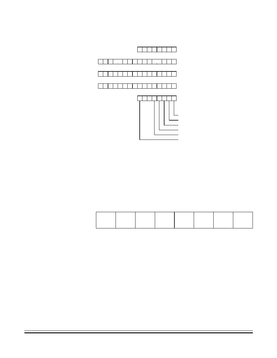
Central Processor Unit (CPU)
CPU Registers
MC68HC908RK2
--
Rev. 4.0
Advance Information
MOTOROLA
Central Processor Unit (CPU)
65
Figure 5-1. CPU Registers
5.4.1 Accumulator
The accumulator is a general-purpose 8-bit register. The CPU uses the
accumulator to hold operands and the results of arithmetic/logic
operations.
5.4.2 Index Register
The 16-bit index register allows indexed addressing of a 64-Kbyte
memory space. H is the upper byte of the index register, and X is the
lower byte. H:X is the concatenated 16-bit index register.
In the indexed addressing modes, the CPU uses the contents of the
index register to determine the conditional address of the operand.
ACCUMULATOR (A)
INDEX REGISTER (H:X)
STACK POINTER (SP)
PROGRAM COUNTER (PC)
CONDITION CODE REGISTER (CCR)
CARRY/BORROW FLAG
ZERO FLAG
NEGATIVE FLAG
INTERRUPT MASK
HALF-CARRY FLAG
TWO'S COMPLEMENT OVERFLOW FLAG
V 1 1 H
I
N Z C
H
X
0
0
0
0
7
15
15
15
7
0
Bit 7
6
5
4
3
2
1
Bit 0
Read:
Write:
Reset:
Unaffected by reset
Figure 5-2. Accumulator (A)
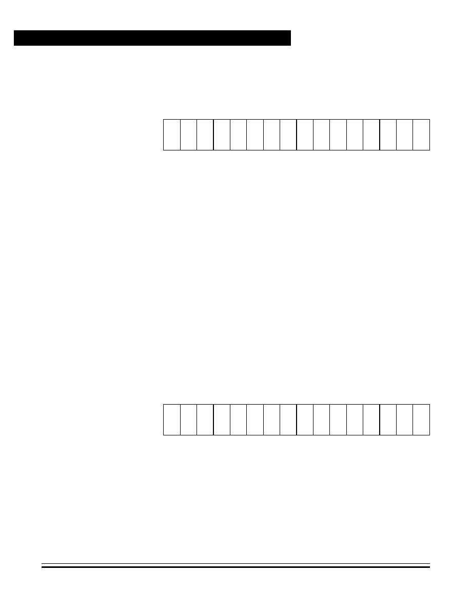
Central Processor Unit (CPU)
Advance Information
MC68HC908RK2
--
Rev. 4.0
66
Central Processor Unit (CPU)
MOTOROLA
The index register can serve also as a temporary data storage location.
5.4.3 Stack Pointer
The stack pointer is a 16-bit register that contains the address of the next
location on the stack. During a reset, the stack pointer is preset to
$00FF. The reset stack pointer (RSP) instruction sets the least
significant byte (LSB) to $FF and does not affect the most significant
byte (MSB). The stack pointer decrements as data is pushed onto the
stack and increments as data is pulled from the stack.
In the stack pointer 8-bit offset and 16-bit offset addressing modes, the
stack pointer can function as an index register to access data on the
stack. The CPU uses the contents of the stack pointer to determine the
conditional address of the operand.
NOTE:
For correct operation, the stack pointer must point only to RAM
locations.
Bit
15
14
13
12
11
10
9
8
7
6
5
4
3
2
1
Bit
0
Read:
Write:
Reset:
0
0
0
0
0
0
0
0
X
X
X
X
X
X
X
X
X = Indeterminate
Figure 5-3. Index Register (H:X)
Bit
15
14
13
12
11
10
9
8
7
6
5
4
3
2
1
Bit
0
Read:
Write:
Reset:
0
0
0
0
0
0
0
0
1
1
1
1
1
1
1
1
Figure 5-4. Stack Pointer (SP)
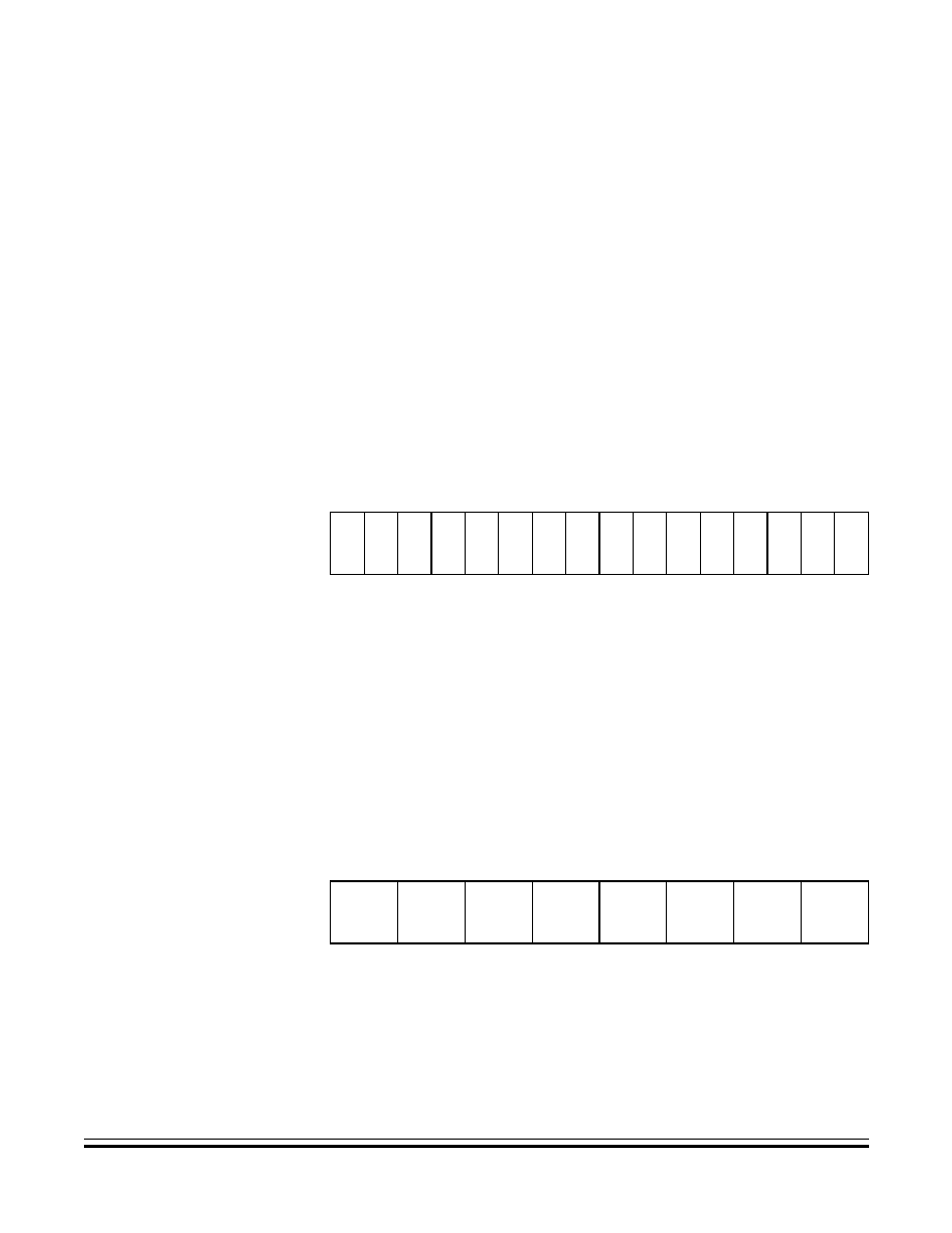
Central Processor Unit (CPU)
CPU Registers
MC68HC908RK2
--
Rev. 4.0
Advance Information
MOTOROLA
Central Processor Unit (CPU)
67
5.4.4 Program Counter
The program counter is a 16-bit register that contains the address of the
next instruction or operand to be fetched.
Normally, the program counter automatically increments to the next
sequential memory location every time an instruction or operand is
fetched. Jump, branch, and interrupt operations load the program
counter with an address other than that of the next sequential location.
During reset, the program counter is loaded with the reset vector
address located at $FFFE and $FFFF. The vector address is the
address of the first instruction to be executed after exiting the reset state.
5.4.5 Condition Code Register
The 8-bit condition code register contains the interrupt mask and five
flags that indicate the results of the instruction just executed. Bits 6 and
5 are set permanently to logic 1. The following paragraphs describe the
functions of the condition code register.
Bit
15
14
13
12
11
10
9
8
7
6
5
4
3
2
1
Bit
0
Read:
Write:
Reset:
Loaded with vector from $FFFE and $FFFF
Figure 5-5. Program Counter (PC)
Bit 7
6
5
4
3
2
1
Bit 0
Read:
V
1
1
H
I
N
Z
C
Write:
Reset:
X
1
1
X
1
X
X
X
X = Indeterminate
Figure 5-6. Condition Code Register (CCR)

Central Processor Unit (CPU)
Advance Information
MC68HC908RK2
--
Rev. 4.0
68
Central Processor Unit (CPU)
MOTOROLA
V -- Overflow Flag
The CPU sets the overflow flag when a two's complement overflow
occurs. The signed branch instructions BGT, BGE, BLE, and BLT use
the overflow flag.
1 = Overflow
0 = No overflow
H -- Half-Carry Flag
The CPU sets the half-carry flag when a carry occurs between
accumulator bits 3 and 4 during an add-without-carry (ADD) or
add-with-carry (ADC) operation. The half-carry flag is required for
binary-coded decimal (BCD) arithmetic operations. The DAA
instruction uses the states of the H and C flags to determine the
appropriate correction factor.
1 = Carry between bits 3 and 4
0 = No carry between bits 3 and 4
I -- Interrupt Mask
When the interrupt mask is set, all maskable CPU interrupts are
disabled. CPU interrupts are enabled when the interrupt mask is
cleared. When a CPU interrupt occurs, the interrupt mask is set
automatically after the CPU registers are saved on the stack, but
before the interrupt vector is fetched.
1 = Interrupts disabled
0 = Interrupts enabled
NOTE:
To maintain M6805 compatibility, the upper byte of the index register (H)
is not stacked automatically. If the interrupt service routine modifies H,
then the user must stack and unstack H using the PSHH and PULH
instructions.
After the I bit is cleared, the highest-priority interrupt request is
serviced first.
A return-from-interrupt (RTI) instruction pulls the CPU registers from
the stack and restores the interrupt mask from the stack. After any
reset, the interrupt mask is set and can be cleared only by the clear
interrupt mask software instruction (CLI).

Central Processor Unit (CPU)
Arithmetic/Logic Unit (ALU)
MC68HC908RK2
--
Rev. 4.0
Advance Information
MOTOROLA
Central Processor Unit (CPU)
69
N -- Negative Flag
The CPU sets the negative flag when an arithmetic operation, logic
operation, or data manipulation produces a negative result, setting bit
7 of the result.
1 = Negative result
0 = Non-negative result
Z -- Zero Flag
The CPU sets the zero flag when an arithmetic operation, logic
operation, or data manipulation produce a result of $00.
1 = Zero result
0 = Non-zero result
C -- Carry/Borrow Flag
The CPU sets the carry/borrow flag when an addition operation
produces a carry out of bit 7 of the accumulator or when a subtraction
operation requires a borrow. Some instructions -- such as bit test and
branch, shift, and rotate -- also clear or set the carry/borrow flag.
1 = Carry out of bit 7
0 = No carry out of bit 7
5.5 Arithmetic/Logic Unit (ALU)
The ALU performs the arithmetic and logic operations defined by the
instruction set.
Refer to the CPU08 Reference Manual, Motorola document oeswe
number CPU08RM/AD, for a description of the instructions and
addressing modes and more detail about the architecture of the CPU.
5.6 Low-Power Modes
The WAIT and STOP instructions put the MCU in low
power-consumption standby modes.

Central Processor Unit (CPU)
Advance Information
MC68HC908RK2
--
Rev. 4.0
70
Central Processor Unit (CPU)
MOTOROLA
5.6.1 Wait Mode
The WAIT instruction:
∑
Clears the interrupt mask (I bit) in the condition code register,
enabling interrupts. After exit from wait mode by interrupt, the I bit
remains clear. After exit by reset, the I bit is set.
∑
Disables the CPU clock
5.6.2 Stop Mode
The STOP instruction:
∑
Clears the interrupt mask (I bit) in the condition code register,
enabling external interrupts. After exit from stop mode by external
interrupt, the I bit remains clear. After exit by reset, the I bit is set.
∑
Disables the CPU clock
After exiting stop mode, the CPU clock begins running after the oscillator
stabilization delay.
5.7 CPU During Break Interrupts
If the break module is enabled, a break interrupt causes the CPU to
execute the software interrupt instruction (SWI) at the completion of the
current CPU instruction. (See
Section 7. Break Module (BRK)
.) The
program counter vectors to $FFFC≠$FFFD ($FEFC≠$FEFD in monitor
mode).
A return-from-interrupt instruction (RTI) in the break routine ends the
break interrupt and returns the MCU to normal operation if the break
interrupt has been deasserted.
5.8 Instruction Set Summary
Table 5-1
provides a summary of the M68HC08 instruction set.
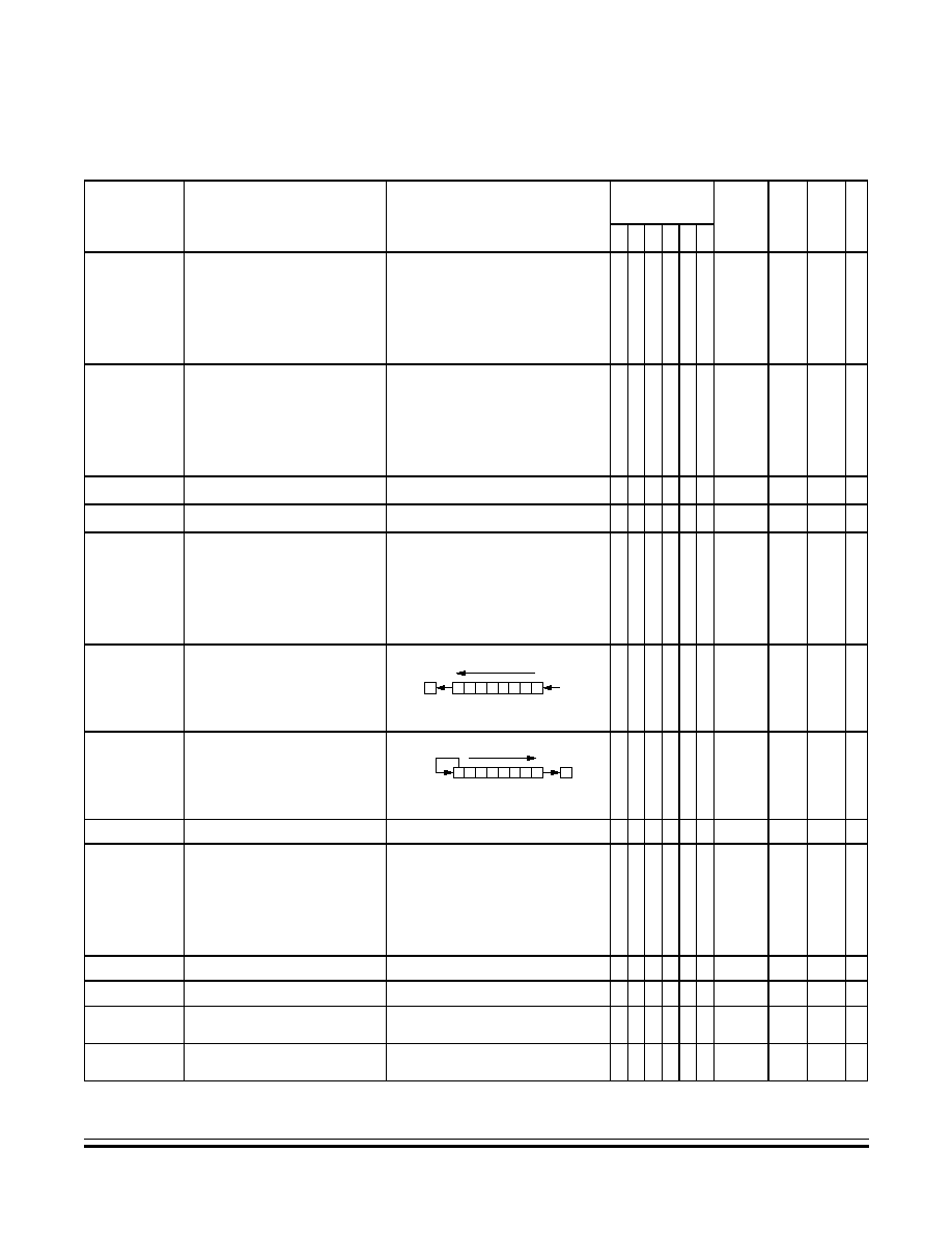
Central Processor Unit (CPU)
Instruction Set Summary
MC68HC908RK2
--
Rev. 4.0
Advance Information
MOTOROLA
Central Processor Unit (CPU)
71
Table 5-1. Instruction Set Summary (Sheet 1 of 7)
Source
Form
Operation
Description
Effect
on CCR
Ad
d
r
ess
Mod
e
Op
c
o
d
e
O
p
er
an
d
Cy
cl
es
V H I N Z C
ADC #opr
ADC opr
ADC opr
ADC opr,X
ADC opr,X
ADC ,X
ADC opr,SP
ADC opr,SP
Add with Carry
A
(A) + (M) + (C)
≠
IMM
DIR
EXT
IX2
IX1
IX
SP1
SP2
A9
B9
C9
D9
E9
F9
9EE9
9ED9
ii
dd
hh ll
ee ff
ff
ff
ee ff
2
3
4
4
3
2
4
5
ADD #opr
ADD opr
ADD opr
ADD opr,X
ADD opr,X
ADD ,X
ADD opr,SP
ADD opr,SP
Add without Carry
A
(A) + (M)
≠
IMM
DIR
EXT
IX2
IX1
IX
SP1
SP2
AB
BB
CB
DB
EB
FB
9EEB
9EDB
ii
dd
hh ll
ee ff
ff
ff
ee ff
2
3
4
4
3
2
4
5
AIS #opr
Add Immediate Value (Signed) to SP
SP
(SP) + (16
´
M)
≠ ≠ ≠ ≠ ≠ ≠ IMM
A7
ii 2
AIX #opr
Add Immediate Value (Signed) to H:X
H:X
(H:X) + (16
´
M)
≠ ≠ ≠ ≠ ≠ ≠ IMM
AF
ii
2
AND #opr
AND opr
AND opr
AND opr,X
AND opr,X
AND ,X
AND opr,SP
AND opr,SP
Logical AND
A
(A) & (M)
0 ≠ ≠
≠
IMM
DIR
EXT
IX2
IX1
IX
SP1
SP2
A4
B4
C4
D4
E4
F4
9EE4
9ED4
ii
dd
hh ll
ee ff
ff
ff
ee ff
2
3
4
4
3
2
4
5
ASL opr
ASLA
ASLX
ASL opr,X
ASL ,X
ASL opr,SP
Arithmetic Shift Left
(Same as LSL)
≠ ≠
DIR
INH
INH
IX1
IX
SP1
38
48
58
68
78
9E68
dd
ff
ff
4
1
1
4
3
5
ASR opr
ASRA
ASRX
ASR opr,X
ASR opr,X
ASR opr,SP
Arithmetic Shift Right
≠ ≠
DIR
INH
INH
IX1
IX
SP1
37
47
57
67
77
9E67
dd
ff
ff
4
1
1
4
3
5
BCC rel
Branch if Carry Bit Clear
PC
(PC) + 2 + rel ? (C) = 0
≠ ≠ ≠ ≠ ≠ ≠ REL
24
rr
3
BCLR n, opr
Clear Bit n in M
Mn
0
≠ ≠ ≠ ≠ ≠ ≠
DIR (b0)
DIR (b1)
DIR (b2)
DIR (b3)
DIR (b4)
DIR (b5)
DIR (b6)
DIR (b7)
11
13
15
17
19
1B
1D
1F
dd
dd
dd
dd
dd
dd
dd
dd
4
4
4
4
4
4
4
4
BCS rel
Branch if Carry Bit Set (Same as BLO)
PC
(PC) + 2 + rel ? (C) = 1
≠ ≠ ≠ ≠ ≠ ≠ REL
25
rr
3
BEQ rel
Branch if Equal
PC
(PC) + 2 + rel ? (Z) = 1
≠ ≠ ≠ ≠ ≠ ≠ REL
27
rr
3
BGE opr
Branch if Greater Than or Equal To
(Signed Operands)
PC
(PC) + 2 + rel ? (N
V
) = 0
≠ ≠ ≠ ≠ ≠ ≠ REL
90
rr
3
BGT opr
Branch if Greater Than (Signed
Operands)
PC
(PC) + 2 + rel ? (Z)
| (N
V
) = 0
≠ ≠ ≠ ≠ ≠ ≠ REL
92
rr
3
C
b0
b7
0
b0
b7
C
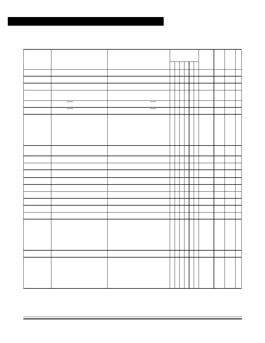
Central Processor Unit (CPU)
Advance Information
MC68HC908RK2
--
Rev. 4.0
72
Central Processor Unit (CPU)
MOTOROLA
BHCC rel
Branch if Half Carry Bit Clear
PC
(PC) + 2 + rel ? (H) = 0
≠ ≠ ≠ ≠ ≠ ≠ REL
28
rr
3
BHCS rel
Branch if Half Carry Bit Set
PC
(PC) + 2 + rel ? (H) = 1
≠ ≠ ≠ ≠ ≠ ≠ REL
29
rr
3
BHI rel
Branch if Higher
PC
(PC) + 2 + rel ? (C) | (Z) = 0
≠ ≠ ≠ ≠ ≠ ≠ REL
22
rr
3
BHS rel
Branch if Higher or Same
(Same as BCC)
PC
(PC) + 2 + rel ? (C) = 0
≠ ≠ ≠ ≠ ≠ ≠ REL
24
rr
3
BIH rel
Branch if IRQ Pin High
PC
(PC) + 2 + rel ? IRQ = 1
≠ ≠ ≠ ≠ ≠ ≠ REL
2F
rr
3
BIL rel
Branch if IRQ Pin Low
PC
(PC) + 2 + rel ? IRQ = 0
≠ ≠ ≠ ≠ ≠ ≠ REL
2E
rr
3
BIT #opr
BIT opr
BIT opr
BIT opr,X
BIT opr,X
BIT ,X
BIT opr,SP
BIT opr,SP
Bit Test
(A) & (M)
0 ≠ ≠
≠
IMM
DIR
EXT
IX2
IX1
IX
SP1
SP2
A5
B5
C5
D5
E5
F5
9EE5
9ED5
ii
dd
hh ll
ee ff
ff
ff
ee ff
2
3
4
4
3
2
4
5
BLE opr
Branch if Less Than or Equal To
(Signed Operands)
PC
(PC) + 2 + rel ? (Z)
| (N
V
) =
1 ≠ ≠ ≠ ≠ ≠ ≠ REL
93
rr
3
BLO rel
Branch if Lower (Same as BCS)
PC
(PC) + 2 + rel ? (C) = 1
≠ ≠ ≠ ≠ ≠ ≠ REL
25
rr
3
BLS rel
Branch if Lower or Same
PC
(PC) + 2 + rel ? (C) | (Z) = 1
≠ ≠ ≠ ≠ ≠ ≠ REL
23
rr
3
BLT opr
Branch if Less Than (Signed Operands)
PC
(PC) + 2 + rel ? (N
V
) =
1
≠ ≠ ≠ ≠ ≠ ≠ REL
91
rr
3
BMC rel
Branch if Interrupt Mask Clear
PC
(PC) + 2 + rel ? (I) = 0
≠ ≠ ≠ ≠ ≠ ≠ REL
2C
rr
3
BMI rel
Branch if Minus
PC
(PC) + 2 + rel ? (N) = 1
≠ ≠ ≠ ≠ ≠ ≠ REL
2B
rr
3
BMS rel
Branch if Interrupt Mask Set
PC
(PC) + 2 + rel ? (I) = 1
≠ ≠ ≠ ≠ ≠ ≠ REL
2D
rr
3
BNE rel
Branch if Not Equal
PC
(PC) + 2 + rel ? (Z) = 0
≠ ≠ ≠ ≠ ≠ ≠ REL
26
rr
3
BPL rel
Branch if Plus
PC
(PC) + 2 + rel ? (N) = 0
≠ ≠ ≠ ≠ ≠ ≠ REL
2A
rr
3
BRA rel
Branch Always
PC
(PC) + 2 + rel
≠ ≠ ≠ ≠ ≠ ≠ REL
20
rr
3
BRCLR n,opr,rel Branch if Bit n in M Clear
PC
(PC) + 3 + rel ? (Mn) = 0
≠ ≠ ≠ ≠ ≠
DIR (b0)
DIR (b1)
DIR (b2)
DIR (b3)
DIR (b4)
DIR (b5)
DIR (b6)
DIR (b7)
01
03
05
07
09
0B
0D
0F
dd rr
dd rr
dd rr
dd rr
dd rr
dd rr
dd rr
dd rr
5
5
5
5
5
5
5
5
BRN rel
Branch Never
PC
(PC) + 2
≠ ≠ ≠ ≠ ≠ ≠ REL
21
rr
3
BRSET n,opr,rel Branch if Bit n in M Set
PC
(PC) + 3 + rel ? (Mn) = 1
≠ ≠ ≠ ≠ ≠
DIR (b0)
DIR (b1)
DIR (b2)
DIR (b3)
DIR (b4)
DIR (b5)
DIR (b6)
DIR (b7)
00
02
04
06
08
0A
0C
0E
dd rr
dd rr
dd rr
dd rr
dd rr
dd rr
dd rr
dd rr
5
5
5
5
5
5
5
5
Table 5-1. Instruction Set Summary (Sheet 2 of 7)
Source
Form
Operation
Description
Effect
on CCR
Ad
d
r
ess
Mo
de
Op
cod
e
Op
eran
d
Cycl
es
V H I N Z C
Central Processor Unit (CPU)
Instruction Set Summary
MC68HC908RK2
--
Rev. 4.0
Advance Information
MOTOROLA
Central Processor Unit (CPU)
73
BSET n,opr
Set Bit n in M
Mn
1
≠ ≠ ≠ ≠ ≠ ≠
DIR (b0)
DIR (b1)
DIR (b2)
DIR (b3)
DIR (b4)
DIR (b5)
DIR (b6)
DIR (b7)
10
12
14
16
18
1A
1C
1E
dd
dd
dd
dd
dd
dd
dd
dd
4
4
4
4
4
4
4
4
BSR rel
Branch to Subroutine
PC
(PC) + 2; push (PCL)
SP
(SP) ≠ 1; push (PCH)
SP
(SP) ≠ 1
PC
(PC) + rel
≠ ≠ ≠ ≠ ≠ ≠ REL
AD
rr
4
CBEQ opr,rel
CBEQA #opr,rel
CBEQX #opr,rel
CBEQ opr,X+,rel
CBEQ X+,rel
CBEQ opr,SP,rel
Compare and Branch if Equal
PC
(PC) + 3 + rel ? (A) ≠ (M) = $00
PC
(PC) + 3 + rel ? (A) ≠ (M) = $00
PC
(PC) + 3 + rel ? (X) ≠ (M) = $00
PC
(PC) + 3 + rel ? (A) ≠ (M) = $00
PC
(PC) + 2 + rel ? (A) ≠ (M) = $00
PC
(PC) + 4 + rel ? (A) ≠ (M) = $00
≠ ≠ ≠ ≠ ≠ ≠
DIR
IMM
IMM
IX1+
IX+
SP1
31
41
51
61
71
9E61
dd rr
ii rr
ii rr
ff rr
rr
ff rr
5
4
4
5
4
6
CLC
Clear Carry Bit
C
0
≠ ≠ ≠ ≠ ≠ 0 INH
98
1
CLI
Clear Interrupt Mask
I
0
≠ ≠ 0 ≠ ≠ ≠ INH
9A
2
CLR opr
CLRA
CLRX
CLRH
CLR opr,X
CLR ,X
CLR opr,SP
Clear
M
$00
A
$00
X
$00
H
$00
M
$00
M
$00
M
$00
0 ≠ ≠ 0 1 ≠
DIR
INH
INH
INH
IX1
IX
SP1
3F
4F
5F
8C
6F
7F
9E6F
dd
ff
ff
3
1
1
1
3
2
4
CMP #opr
CMP opr
CMP opr
CMP opr,X
CMP opr,X
CMP ,X
CMP opr,SP
CMP opr,SP
Compare A with M
(A) ≠ (M)
≠ ≠
IMM
DIR
EXT
IX2
IX1
IX
SP1
SP2
A1
B1
C1
D1
E1
F1
9EE1
9ED1
ii
dd
hh ll
ee ff
ff
ff
ee ff
2
3
4
4
3
2
4
5
COM opr
COMA
COMX
COM opr,X
COM ,X
COM opr,SP
Complement (One's Complement)
M
(M) = $FF ≠ (M)
A
(A) = $FF ≠ (M)
X
(X) = $FF ≠ (M)
M
(M) = $FF ≠ (M)
M
(M) = $FF ≠ (M)
M
(M) = $FF ≠ (M)
0 ≠ ≠
1
DIR
INH
INH
IX1
IX
SP1
33
43
53
63
73
9E63
dd
ff
ff
4
1
1
4
3
5
CPHX #opr
CPHX opr
Compare H:X with M
(H:X) ≠ (M:M + 1)
≠ ≠
IMM
DIR
65
75
ii ii+1
dd
3
4
CPX #opr
CPX opr
CPX opr
CPX ,X
CPX opr,X
CPX opr,X
CPX opr,SP
CPX opr,SP
Compare X with M
(X) ≠ (M)
≠ ≠
IMM
DIR
EXT
IX2
IX1
IX
SP1
SP2
A3
B3
C3
D3
E3
F3
9EE3
9ED3
ii
dd
hh ll
ee ff
ff
ff
ee ff
2
3
4
4
3
2
4
5
DAA
Decimal Adjust A
(A)
10
U ≠ ≠
INH
72
2
Table 5-1. Instruction Set Summary (Sheet 3 of 7)
Source
Form
Operation
Description
Effect
on CCR
Ad
d
r
ess
Mo
de
Op
cod
e
Op
eran
d
Cycl
es
V H I N Z C
Central Processor Unit (CPU)
Advance Information
MC68HC908RK2
--
Rev. 4.0
74
Central Processor Unit (CPU)
MOTOROLA
DBNZ opr,rel
DBNZA rel
DBNZX rel
DBNZ opr,X,rel
DBNZ X,rel
DBNZ opr,SP,rel
Decrement and Branch if Not Zero
A
(A) ≠ 1 or M
(M) ≠ 1 or X
(X) ≠ 1
PC
(PC) + 3 + rel ? (result)
0
PC
(PC) + 2 + rel ? (result)
0
PC
(PC) + 2 + rel ? (result)
0
PC
(PC) + 3 + rel ? (result)
0
PC
(PC) + 2 + rel ? (result)
0
PC
(PC) + 4 + rel ? (result)
0
≠ ≠ ≠ ≠ ≠ ≠
DIR
INH
INH
IX1
IX
SP1
3B
4B
5B
6B
7B
9E6B
dd rr
rr
rr
ff rr
rr
ff rr
5
3
3
5
4
6
DEC opr
DECA
DECX
DEC opr,X
DEC ,X
DEC opr,SP
Decrement
M
(M) ≠ 1
A
(A) ≠ 1
X
(X) ≠ 1
M
(M) ≠ 1
M
(M) ≠ 1
M
(M) ≠ 1
≠ ≠
≠
DIR
INH
INH
IX1
IX
SP1
3A
4A
5A
6A
7A
9E6A
dd
ff
ff
4
1
1
4
3
5
DIV
Divide
A
(H:A)/(X)
H
Remainder
≠ ≠ ≠ ≠
INH
52
7
EOR #opr
EOR opr
EOR opr
EOR opr,X
EOR opr,X
EOR ,X
EOR opr,SP
EOR opr,SP
Exclusive OR M with A
A
(A
M)
0 ≠ ≠
≠
IMM
DIR
EXT
IX2
IX1
IX
SP1
SP2
A8
B8
C8
D8
E8
F8
9EE8
9ED8
ii
dd
hh ll
ee ff
ff
ff
ee ff
2
3
4
4
3
2
4
5
INC opr
INCA
INCX
INC opr,X
INC ,X
INC opr,SP
Increment
M
(M) + 1
A
(A) + 1
X
(X) + 1
M
(M) + 1
M
(M) + 1
M
(M) + 1
≠ ≠
≠
DIR
INH
INH
IX1
IX
SP1
3C
4C
5C
6C
7C
9E6C
dd
ff
ff
4
1
1
4
3
5
JMP opr
JMP opr
JMP opr,X
JMP opr,X
JMP ,X
Jump
PC
Jump Address
≠ ≠ ≠ ≠ ≠ ≠
DIR
EXT
IX2
IX1
IX
BC
CC
DC
EC
FC
dd
hh ll
ee ff
ff
2
3
4
3
2
JSR opr
JSR opr
JSR opr,X
JSR opr,X
JSR ,X
Jump to Subroutine
PC
(PC) + n (n = 1, 2, or 3)
Push (PCL); SP
(SP) ≠ 1
Push (PCH); SP
(SP) ≠ 1
PC
Unconditional Address
≠ ≠ ≠ ≠ ≠ ≠
DIR
EXT
IX2
IX1
IX
BD
CD
DD
ED
FD
dd
hh ll
ee ff
ff
4
5
6
5
4
LDA #opr
LDA opr
LDA opr
LDA opr,X
LDA opr,X
LDA ,X
LDA opr,SP
LDA opr,SP
Load A from M
A
(M)
0 ≠ ≠
≠
IMM
DIR
EXT
IX2
IX1
IX
SP1
SP2
A6
B6
C6
D6
E6
F6
9EE6
9ED6
ii
dd
hh ll
ee ff
ff
ff
ee ff
2
3
4
4
3
2
4
5
LDHX #opr
LDHX opr
Load H:X from M
H:X
(
M:M
+ 1
)
0 ≠ ≠
≠
IMM
DIR
45
55
ii jj
dd
3
4
LDX #opr
LDX opr
LDX opr
LDX opr,X
LDX opr,X
LDX ,X
LDX opr,SP
LDX opr,SP
Load X from M
X
(M)
0 ≠ ≠
≠
IMM
DIR
EXT
IX2
IX1
IX
SP1
SP2
AE
BE
CE
DE
EE
FE
9EEE
9EDE
ii
dd
hh ll
ee ff
ff
ff
ee ff
2
3
4
4
3
2
4
5
Table 5-1. Instruction Set Summary (Sheet 4 of 7)
Source
Form
Operation
Description
Effect
on CCR
Ad
d
r
ess
Mo
de
Op
cod
e
Op
eran
d
Cycl
es
V H I N Z C

Central Processor Unit (CPU)
Instruction Set Summary
MC68HC908RK2
--
Rev. 4.0
Advance Information
MOTOROLA
Central Processor Unit (CPU)
75
LSL opr
LSLA
LSLX
LSL opr,X
LSL ,X
LSL opr,SP
Logical Shift Left
(Same as ASL)
≠ ≠
DIR
INH
INH
IX1
IX
SP1
38
48
58
68
78
9E68
dd
ff
ff
4
1
1
4
3
5
LSR opr
LSRA
LSRX
LSR opr,X
LSR ,X
LSR opr,SP
Logical Shift Right
≠ ≠ 0
DIR
INH
INH
IX1
IX
SP1
34
44
54
64
74
9E64
dd
ff
ff
4
1
1
4
3
5
MOV opr,opr
MOV opr,X+
MOV #opr,opr
MOV X+,opr
Move
(M)
Destination
(M)
Source
H:X
(H:X) + 1 (IX+D, DIX+)
0 ≠ ≠
≠
DD
DIX+
IMD
IX+D
4E
5E
6E
7E
dd dd
dd
ii dd
dd
5
4
4
4
MUL
Unsigned multiply
X:A
(X)
◊
(A)
≠ 0 ≠ ≠ ≠ 0 INH
42
5
NEG opr
NEGA
NEGX
NEG opr,X
NEG ,X
NEG opr,SP
Negate (Two's Complement)
M
≠(M) = $00 ≠ (M)
A
≠(A) = $00 ≠ (A)
X
≠(X) = $00 ≠ (X)
M
≠(M) = $00 ≠ (M)
M
≠(M) = $00 ≠ (M)
≠ ≠
DIR
INH
INH
IX1
IX
SP1
30
40
50
60
70
9E60
dd
ff
ff
4
1
1
4
3
5
NOP
No Operation
None
≠ ≠ ≠ ≠ ≠ ≠ INH
9D
1
NSA
Nibble Swap A
A
(A[3:0]:A[7:4])
≠ ≠ ≠ ≠ ≠ ≠ INH
62
3
ORA #opr
ORA opr
ORA opr
ORA opr,X
ORA opr,X
ORA ,X
ORA opr,SP
ORA opr,SP
Inclusive OR A and M
A
(A) | (M)
0 ≠ ≠
≠
IMM
DIR
EXT
IX2
IX1
IX
SP1
SP2
AA
BA
CA
DA
EA
FA
9EEA
9EDA
ii
dd
hh ll
ee ff
ff
ff
ee ff
2
3
4
4
3
2
4
5
PSHA
Push A onto Stack
Push (A); SP
(SP
) ≠
1
≠ ≠ ≠ ≠ ≠ ≠ INH
87
2
PSHH
Push H onto Stack
Push (H)
;
SP
(SP
) ≠
1
≠ ≠ ≠ ≠ ≠ ≠ INH
8B
2
PSHX
Push X onto Stack
Push (X)
;
SP
(SP
) ≠
1
≠ ≠ ≠ ≠ ≠ ≠ INH
89
2
PULA
Pull A from Stack
SP
(SP +
1); Pull
(
A
)
≠ ≠ ≠ ≠ ≠ ≠ INH
86
2
PULH
Pull H from Stack
SP
(SP +
1); Pull
(
H
)
≠ ≠ ≠ ≠ ≠ ≠ INH
8A
2
PULX
Pull X from Stack
SP
(SP +
1); Pull
(
X
)
≠ ≠ ≠ ≠ ≠ ≠ INH
88
2
ROL opr
ROLA
ROLX
ROL opr,X
ROL ,X
ROL opr,SP
Rotate Left through Carry
≠ ≠
DIR
INH
INH
IX1
IX
SP1
39
49
59
69
79
9E69
dd
ff
ff
4
1
1
4
3
5
ROR opr
RORA
RORX
ROR opr,X
ROR ,X
ROR opr,SP
Rotate Right through Carry
≠ ≠
DIR
INH
INH
IX1
IX
SP1
36
46
56
66
76
9E66
dd
ff
ff
4
1
1
4
3
5
Table 5-1. Instruction Set Summary (Sheet 5 of 7)
Source
Form
Operation
Description
Effect
on CCR
Ad
d
r
ess
Mo
de
Op
cod
e
Op
eran
d
Cycl
es
V H I N Z C
C
b0
b7
0
b0
b7
C
0
C
b0
b7
b0
b7
C
Central Processor Unit (CPU)
Advance Information
MC68HC908RK2
--
Rev. 4.0
76
Central Processor Unit (CPU)
MOTOROLA
RSP
Reset Stack Pointer
SP
$FF
≠ ≠ ≠ ≠ ≠ ≠ INH
9C
1
RTI
Return from Interrupt
SP
(SP) + 1; Pull (CCR)
SP
(SP) + 1; Pull (A)
SP
(SP) + 1; Pull (X)
SP
(SP) + 1; Pull (PCH)
SP
(SP) + 1; Pull (PCL)
INH
80
7
RTS
Return from Subroutine
SP
SP + 1
;
Pull
(
PCH)
SP
SP + 1; Pull (PCL)
≠ ≠ ≠ ≠ ≠ ≠ INH
81
4
SBC #opr
SBC opr
SBC opr
SBC opr,X
SBC opr,X
SBC ,X
SBC opr,SP
SBC opr,SP
Subtract with Carry
A
(A) ≠ (M) ≠ (C)
≠ ≠
IMM
DIR
EXT
IX2
IX1
IX
SP1
SP2
A2
B2
C2
D2
E2
F2
9EE2
9ED2
ii
dd
hh ll
ee ff
ff
ff
ee ff
2
3
4
4
3
2
4
5
SEC
Set Carry Bit
C
1
≠ ≠ ≠ ≠ ≠ 1 INH
99
1
SEI
Set Interrupt Mask
I
1
≠ ≠ 1 ≠ ≠ ≠ INH
9B
2
STA opr
STA opr
STA opr,X
STA opr,X
STA ,X
STA opr,SP
STA opr,SP
Store A in M
M
(A)
0 ≠ ≠
≠
DIR
EXT
IX2
IX1
IX
SP1
SP2
B7
C7
D7
E7
F7
9EE7
9ED7
dd
hh ll
ee ff
ff
ff
ee ff
3
4
4
3
2
4
5
STHX opr
Store H:X in M
(M:M + 1)
(H:X)
0 ≠ ≠
≠ DIR
35
dd
4
STOP
Enable IRQ Pin; Stop Oscillator
I
0; Stop Oscillator
≠ ≠ 0 ≠ ≠ ≠ INH
8E
1
STX opr
STX opr
STX opr,X
STX opr,X
STX ,X
STX opr,SP
STX opr,SP
Store X in M
M
(X)
0 ≠ ≠
≠
DIR
EXT
IX2
IX1
IX
SP1
SP2
BF
CF
DF
EF
FF
9EEF
9EDF
dd
hh ll
ee ff
ff
ff
ee ff
3
4
4
3
2
4
5
SUB #opr
SUB opr
SUB opr
SUB opr,X
SUB opr,X
SUB ,X
SUB opr,SP
SUB opr,SP
Subtract A
(A)
≠
(M)
≠ ≠
IMM
DIR
EXT
IX2
IX1
IX
SP1
SP2
A0
B0
C0
D0
E0
F0
9EE0
9ED0
ii
dd
hh ll
ee ff
ff
ff
ee ff
2
3
4
4
3
2
4
5
SWI
Software Interrupt
PC
(PC) + 1; Push (PCL)
SP
(SP) ≠ 1; Push (PCH)
SP
(SP) ≠ 1; Push (X)
SP
(SP) ≠ 1; Push (A)
SP
(SP) ≠ 1; Push (CCR)
SP
(SP) ≠ 1; I
1
PCH
Interrupt Vector High Byte
PCL
Interrupt Vector Low Byte
≠ ≠ 1 ≠ ≠ ≠ INH
83
9
TAP
Transfer A to CCR
CCR
(A)
INH
84
2
TAX
Transfer A to X
X
(A)
≠ ≠ ≠ ≠ ≠ ≠ INH
97
1
Table 5-1. Instruction Set Summary (Sheet 6 of 7)
Source
Form
Operation
Description
Effect
on CCR
Ad
d
r
ess
Mo
de
Op
cod
e
Op
eran
d
Cycl
es
V H I N Z C
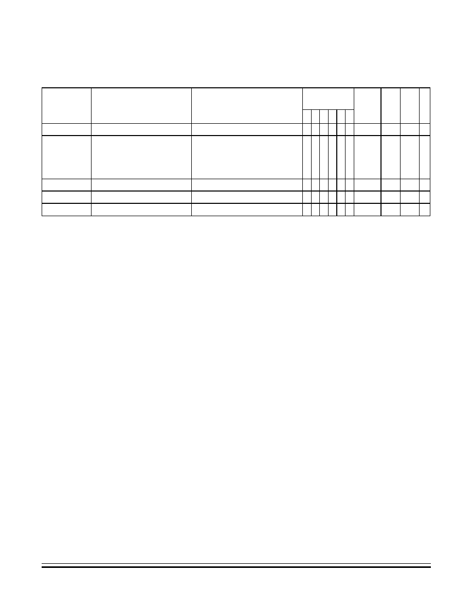
Central Processor Unit (CPU)
Opcode Map
MC68HC908RK2
--
Rev. 4.0
Advance Information
MOTOROLA
Central Processor Unit (CPU)
77
5.9 Opcode Map
The opcode map is provided in
Table 5-2
.
TPA
Transfer CCR to A
A
(CCR)
≠ ≠ ≠ ≠ ≠ ≠ INH
85
1
TST opr
TSTA
TSTX
TST opr,X
TST ,X
TST opr,SP
Test for Negative or Zero
(A) ≠ $00 or (X) ≠ $00 or (M) ≠ $00
0 ≠ ≠
≠
DIR
INH
INH
IX1
IX
SP1
3D
4D
5D
6D
7D
9E6D
dd
ff
ff
3
1
1
3
2
4
TSX
Transfer SP to H:X
H:X
(SP) + 1
≠ ≠ ≠ ≠ ≠ ≠ INH
95
2
TXA
Transfer X to A
A
(X)
≠ ≠ ≠ ≠ ≠ ≠ INH
9F
1
TXS
Transfer H:X to SP
(SP)
(H:X) ≠ 1
≠ ≠ ≠ ≠ ≠ ≠ INH
94
2
A
Accumulator
n
Any bit
C
Carry/borrow bit
opr
Operand (one or two bytes)
CCR
Condition code register
PC
Program counter
dd
Direct address of operand
PCH Program counter high byte
dd rr
Direct address of operand and relative offset of branch instruction
PCL Program counter low byte
DD
Direct to direct addressing mode
REL Relative addressing mode
DIR
Direct addressing mode
rel
Relative program counter offset byte
DIX+
Direct to indexed with post increment addressing mode
rr
Relative program counter offset byte
ee ff
High and low bytes of offset in indexed, 16-bit offset addressing
SP1 Stack pointer, 8-bit offset addressing mode
EXT
Extended addressing mode
SP2 Stack pointer 16-bit offset addressing mode
ff
Offset byte in indexed, 8-bit offset addressing
SP
Stack pointer
H
Half-carry bit
U
Undefined
H
Index register high byte
V
Overflow bit
hh ll
High and low bytes of operand address in extended addressing
X
Index register low byte
I
Interrupt mask
Z
Zero bit
ii
Immediate operand byte
&
Logical AND
IMD
Immediate source to direct destination addressing mode
|
Logical OR
IMM
Immediate addressing mode
Logical EXCLUSIVE OR
INH
Inherent addressing mode
( )
Contents of
IX
Indexed, no offset addressing mode
≠( )
Negation (two's complement)
IX+
Indexed, no offset, post increment addressing mode
#
Immediate value
IX+D
Indexed with post increment to direct addressing mode
´
Sign extend
IX1
Indexed, 8-bit offset addressing mode
Loaded with
IX1+
Indexed, 8-bit offset, post increment addressing mode
?
If
IX2
Indexed, 16-bit offset addressing mode
:
Concatenated with
M
Memory location
Set or cleared
N
Negative bit
--
Not affected
Table 5-1. Instruction Set Summary (Sheet 7 of 7)
Source
Form
Operation
Description
Effect
on CCR
Ad
d
r
ess
Mo
de
Op
cod
e
Op
eran
d
Cycl
es
V H I N Z C
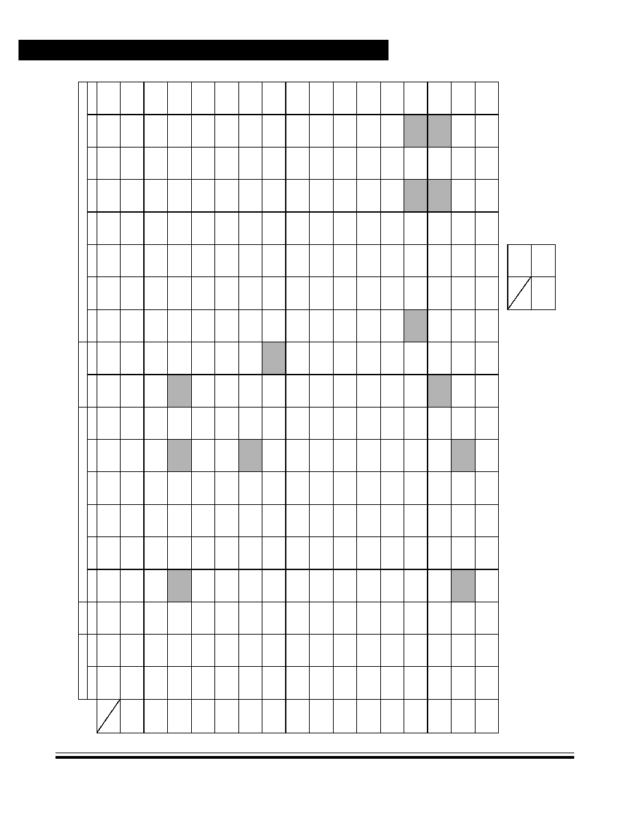
A
d
v
anc
e I
n
f
o
rm
at
i
o
n
M
C68
HC908RK
2
--
Rev. 4.0
78
Cent
ral
P
r
o
c
e
s
sor Uni
t
(CP
U
)
M
O
T
O
R
O
L
A
Ce
n
t
r
a
l P
r
oc
es
s
o
r
U
n
it (CP
U
)
Table 5-2. Opcode Map
Bit Manipulation
Branch
Read-Modify-Write
Control
Register/Memory
DIR
DIR
REL
DIR
INH
INH
IX1
SP1
IX
INH
INH
IMM
DIR
EXT
IX2
SP2
IX1
SP1
IX
0
1
2
3
4
5
6
9E6
7
8
9
A
B
C
D
9ED
E
9EE
F
0
5
BRSET0
3
DIR
4
BSET0
2
DIR
3
BRA
2
REL
4
NEG
2
DIR
1
NEGA
1
INH
1
NEGX
1
INH
4
NEG
2
IX1
5
NEG
3
SP1
3
NEG
1
IX
7
RTI
1
INH
3
BGE
2
REL
2
SUB
2
IMM
3
SUB
2
DIR
4
SUB
3
EXT
4
SUB
3
IX2
5
SUB
4
SP2
3
SUB
2
IX1
4
SUB
3
SP1
2
SUB
1
IX
1
5
BRCLR0
3
DIR
4
BCLR0
2
DIR
3
BRN
2
REL
5
CBEQ
3
DIR
4
CBEQA
3
IMM
4
CBEQX
3
IMM
5
CBEQ
3 IX1+
6
CBEQ
4
SP1
4
CBEQ
2
IX+
4
RTS
1
INH
3
BLT
2
REL
2
CMP
2
IMM
3
CMP
2
DIR
4
CMP
3
EXT
4
CMP
3
IX2
5
CMP
4
SP2
3
CMP
2
IX1
4
CMP
3
SP1
2
CMP
1
IX
2
5
BRSET1
3
DIR
4
BSET1
2
DIR
3
BHI
2
REL
5
MUL
1
INH
7
DIV
1
INH
3
NSA
1
INH
2
DAA
1
INH
3
BGT
2
REL
2
SBC
2
IMM
3
SBC
2
DIR
4
SBC
3
EXT
4
SBC
3
IX2
5
SBC
4
SP2
3
SBC
2
IX1
4
SBC
3
SP1
2
SBC
1
IX
3
5
BRCLR1
3
DIR
4
BCLR1
2
DIR
3
BLS
2
REL
4
COM
2
DIR
1
COMA
1
INH
1
COMX
1
INH
4
COM
2
IX1
5
COM
3
SP1
3
COM
1
IX
9
SWI
1
INH
3
BLE
2
REL
2
CPX
2
IMM
3
CPX
2
DIR
4
CPX
3
EXT
4
CPX
3
IX2
5
CPX
4
SP2
3
CPX
2
IX1
4
CPX
3
SP1
2
CPX
1
IX
4
5
BRSET2
3
DIR
4
BSET2
2
DIR
3
BCC
2
REL
4
LSR
2
DIR
1
LSRA
1
INH
1
LSRX
1
INH
4
LSR
2
IX1
5
LSR
3
SP1
3
LSR
1
IX
2
TAP
1
INH
2
TXS
1
INH
2
AND
2
IMM
3
AND
2
DIR
4
AND
3
EXT
4
AND
3
IX2
5
AND
4
SP2
3
AND
2
IX1
4
AND
3
SP1
2
AND
1
IX
5
5
BRCLR2
3
DIR
4
BCLR2
2
DIR
3
BCS
2
REL
4
STHX
2
DIR
3
LDHX
3
IMM
4
LDHX
2
DIR
3
CPHX
3
IMM
4
CPHX
2
DIR
1
TPA
1
INH
2
TSX
1
INH
2
BIT
2
IMM
3
BIT
2
DIR
4
BIT
3
EXT
4
BIT
3
IX2
5
BIT
4
SP2
3
BIT
2
IX1
4
BIT
3
SP1
2
BIT
1
IX
6
5
BRSET3
3
DIR
4
BSET3
2
DIR
3
BNE
2
REL
4
ROR
2
DIR
1
RORA
1
INH
1
RORX
1
INH
4
ROR
2
IX1
5
ROR
3
SP1
3
ROR
1
IX
2
PULA
1
INH
2
LDA
2
IMM
3
LDA
2
DIR
4
LDA
3
EXT
4
LDA
3
IX2
5
LDA
4
SP2
3
LDA
2
IX1
4
LDA
3
SP1
2
LDA
1
IX
7
5
BRCLR3
3
DIR
4
BCLR3
2
DIR
3
BEQ
2
REL
4
ASR
2
DIR
1
ASRA
1
INH
1
ASRX
1
INH
4
ASR
2
IX1
5
ASR
3
SP1
3
ASR
1
IX
2
PSHA
1
INH
1
TAX
1
INH
2
AIS
2
IMM
3
STA
2
DIR
4
STA
3
EXT
4
STA
3
IX2
5
STA
4
SP2
3
STA
2
IX1
4
STA
3
SP1
2
STA
1
IX
8
5
BRSET4
3
DIR
4
BSET4
2
DIR
3
BHCC
2
REL
4
LSL
2
DIR
1
LSLA
1
INH
1
LSLX
1
INH
4
LSL
2
IX1
5
LSL
3
SP1
3
LSL
1
IX
2
PULX
1
INH
1
CLC
1
INH
2
EOR
2
IMM
3
EOR
2
DIR
4
EOR
3
EXT
4
EOR
3
IX2
5
EOR
4
SP2
3
EOR
2
IX1
4
EOR
3
SP1
2
EOR
1
IX
9
5
BRCLR4
3
DIR
4
BCLR4
2
DIR
3
BHCS
2
REL
4
ROL
2
DIR
1
ROLA
1
INH
1
ROLX
1
INH
4
ROL
2
IX1
5
ROL
3
SP1
3
ROL
1
IX
2
PSHX
1
INH
1
SEC
1
INH
2
ADC
2
IMM
3
ADC
2
DIR
4
ADC
3
EXT
4
ADC
3
IX2
5
ADC
4
SP2
3
ADC
2
IX1
4
ADC
3
SP1
2
ADC
1
IX
A
5
BRSET5
3
DIR
4
BSET5
2
DIR
3
BPL
2
REL
4
DEC
2
DIR
1
DECA
1
INH
1
DECX
1
INH
4
DEC
2
IX1
5
DEC
3
SP1
3
DEC
1
IX
2
PULH
1
INH
2
CLI
1
INH
2
ORA
2
IMM
3
ORA
2
DIR
4
ORA
3
EXT
4
ORA
3
IX2
5
ORA
4
SP2
3
ORA
2
IX1
4
ORA
3
SP1
2
ORA
1
IX
B
5
BRCLR5
3
DIR
4
BCLR5
2
DIR
3
BMI
2
REL
5
DBNZ
3
DIR
3
DBNZA
2
INH
3
DBNZX
2
INH
5
DBNZ
3
IX1
6
DBNZ
4
SP1
4
DBNZ
2
IX
2
PSHH
1
INH
2
SEI
1
INH
2
ADD
2
IMM
3
ADD
2
DIR
4
ADD
3
EXT
4
ADD
3
IX2
5
ADD
4
SP2
3
ADD
2
IX1
4
ADD
3
SP1
2
ADD
1
IX
C
5
BRSET6
3
DIR
4
BSET6
2
DIR
3
BMC
2
REL
4
INC
2
DIR
1
INCA
1
INH
1
INCX
1
INH
4
INC
2
IX1
5
INC
3
SP1
3
INC
1
IX
1
CLRH
1
INH
1
RSP
1
INH
2
JMP
2
DIR
3
JMP
3
EXT
4
JMP
3
IX2
3
JMP
2
IX1
2
JMP
1
IX
D
5
BRCLR6
3
DIR
4
BCLR6
2
DIR
3
BMS
2
REL
3
TST
2
DIR
1
TSTA
1
INH
1
TSTX
1
INH
3
TST
2
IX1
4
TST
3
SP1
2
TST
1
IX
1
NOP
1
INH
4
BSR
2
REL
4
JSR
2
DIR
5
JSR
3
EXT
6
JSR
3
IX2
5
JSR
2
IX1
4
JSR
1
IX
E
5
BRSET7
3
DIR
4
BSET7
2
DIR
3
BIL
2
REL
5
MOV
3
DD
4
MOV
2 DIX+
4
MOV
3
IMD
4
MOV
2 IX+D
1
STOP
1
INH
*
2
LDX
2
IMM
3
LDX
2
DIR
4
LDX
3
EXT
4
LDX
3
IX2
5
LDX
4
SP2
3
LDX
2
IX1
4
LDX
3
SP1
2
LDX
1
IX
F
5
BRCLR7
3
DIR
4
BCLR7
2
DIR
3
BIH
2
REL
3
CLR
2
DIR
1
CLRA
1
INH
1
CLRX
1
INH
3
CLR
2
IX1
4
CLR
3
SP1
2
CLR
1
IX
1
WAIT
1
INH
1
TXA
1
INH
2
AIX
2
IMM
3
STX
2
DIR
4
STX
3
EXT
4
STX
3
IX2
5
STX
4
SP2
3
STX
2
IX1
4
STX
3
SP1
2
STX
1
IX
INH Inherent
REL Relative
SP1 Stack Pointer, 8-Bit Offset
IMM Immediate
IX
Indexed, No Offset
SP2 Stack Pointer, 16-Bit Offset
DIR Direct
IX1
Indexed, 8-Bit Offset
IX+
Indexed, No Offset with
EXT Extended
IX2
Indexed, 16-Bit Offset
Post Increment
DD
Direct-Direct
IMD Immediate-Direct
IX1+ Indexed, 1-Byte Offset with
IX+D Indexed-Direct
DIX+ Direct-Indexed
Post Increment
*
Pre-byte for stack pointer indexed instructions
0
High Byte of Opcode in Hexadecimal
Low Byte of Opcode in Hexadecimal
0
5
BRSET0
3
DIR
Cycles
Opcode Mnemonic
Number of Bytes / Addressing Mode
MSB
LSB
MSB
LSB

MC68HC908RK2
--
Rev. 4.0
Advance Information
MOTOROLA
System Integration Module (SIM)
79
Advance Information -- MC68HC908RK2
Section 6. System Integration Module (SIM)
6.1 Contents
6.2
Introduction . . . . . . . . . . . . . . . . . . . . . . . . . . . . . . . . . . . . . . . . 80
6.3
SIM Bus Clock Control and Generation . . . . . . . . . . . . . . . . . . 83
6.3.1
Bus Timing . . . . . . . . . . . . . . . . . . . . . . . . . . . . . . . . . . . . . .83
6.3.2
Clock Startup from POR or LVI Reset . . . . . . . . . . . . . . . . . 83
6.3.3
Clocks in Stop Mode and Wait Mode . . . . . . . . . . . . . . . . . . 84
6.4
Reset and System Initialization. . . . . . . . . . . . . . . . . . . . . . . . . 84
6.4.1
External Pin Reset . . . . . . . . . . . . . . . . . . . . . . . . . . . . . . . . 85
6.4.2
Active Resets from Internal Sources . . . . . . . . . . . . . . . . . . 86
6.4.2.1
Power-On Reset . . . . . . . . . . . . . . . . . . . . . . . . . . . . . . . 87
6.4.2.2
Computer Operating Properly (COP) Reset. . . . . . . . . . . 88
6.4.2.3
Illegal Opcode Reset . . . . . . . . . . . . . . . . . . . . . . . . . . . . 88
6.4.2.4
Illegal Address Reset . . . . . . . . . . . . . . . . . . . . . . . . . . . . 88
6.4.2.5
Low-Voltage Inhibit (LVI) Reset . . . . . . . . . . . . . . . . . . . .88
6.5
SIM Counter . . . . . . . . . . . . . . . . . . . . . . . . . . . . . . . . . . . . . . . 89
6.5.1
SIM Counter During Power-On Reset . . . . . . . . . . . . . . . . . 89
6.5.2
SIM Counter During Stop Mode Recovery . . . . . . . . . . . . . . 89
6.5.3
SIM Counter and Reset States. . . . . . . . . . . . . . . . . . . . . . . 89
6.6
Program Exception Control. . . . . . . . . . . . . . . . . . . . . . . . . . . . 90
6.6.1
Interrupts . . . . . . . . . . . . . . . . . . . . . . . . . . . . . . . . . . . . . . . 90
6.6.1.1
Hardware Interrupts . . . . . . . . . . . . . . . . . . . . . . . . . . . . .92
6.6.1.2
SWI Instruction. . . . . . . . . . . . . . . . . . . . . . . . . . . . . . . . . 93
6.6.2
Reset . . . . . . . . . . . . . . . . . . . . . . . . . . . . . . . . . . . . . . . . . . 93
6.6.3
Break Interrupts . . . . . . . . . . . . . . . . . . . . . . . . . . . . . . . . . . 93
6.6.4
Status Flag Protection in Break Mode . . . . . . . . . . . . . . . . . 94
6.7
Low-Power Modes . . . . . . . . . . . . . . . . . . . . . . . . . . . . . . . . . . 94
6.7.1
Wait Mode . . . . . . . . . . . . . . . . . . . . . . . . . . . . . . . . . . . . . .94
6.7.2
Stop Mode . . . . . . . . . . . . . . . . . . . . . . . . . . . . . . . . . . . . . .96

System Integration Module (SIM)
Advance Information
MC68HC908RK2
--
Rev. 4.0
80
System Integration Module (SIM)
MOTOROLA
6.8
SIM Registers . . . . . . . . . . . . . . . . . . . . . . . . . . . . . . . . . . . . . .97
6.8.1
SIM Break Status Register . . . . . . . . . . . . . . . . . . . . . . . . . . 97
6.8.2
SIM Reset Status Register . . . . . . . . . . . . . . . . . . . . . . . . . 98
6.8.3
SIM Break Flag Control Register . . . . . . . . . . . . . . . . . . . . . 99
6.2 Introduction
This section describes the system integration module (SIM). Together
with the central processor unit (CPU), the SIM controls all MCU
activities. The SIM is a system state controller that coordinates CPU and
exception timing. A block diagram of the SIM is shown in
Figure 6-1
.
Figure 6-2
is a summary of the SIM input/output (I/O) registers.
The SIM is responsible for:
∑
Bus clock generation and control for CPU and peripherals:
≠
Stop/wait/reset/break entry and recovery
≠
Internal clock control
∑
Master reset control, including power-on reset (POR) and
computer operating properly (COP) timeout
∑
Interrupt control:
≠
Acknowledge timing
≠
Arbitration control timing
≠
Vector address generation
∑
CPU enable/disable timing
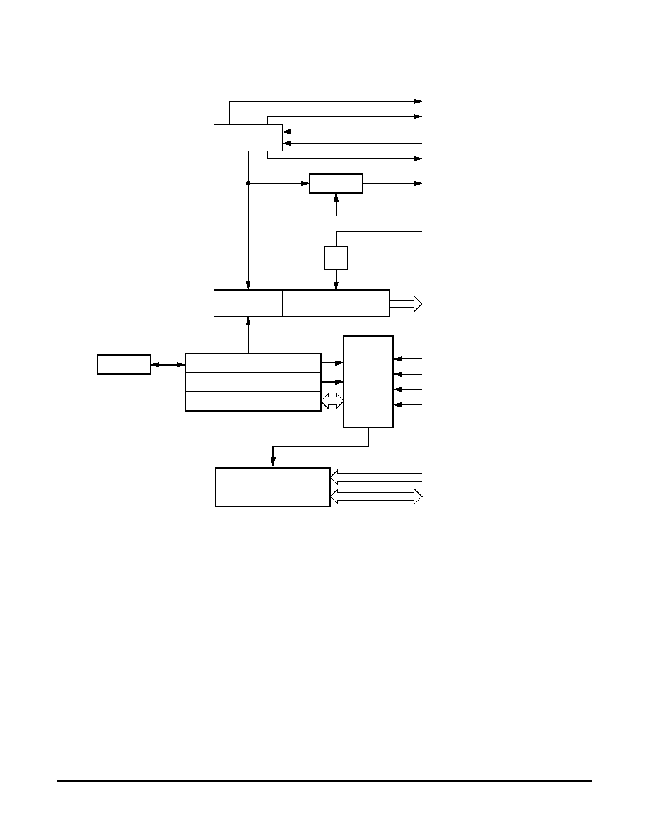
System Integration Module (SIM)
Introduction
MC68HC908RK2
--
Rev. 4.0
Advance Information
MOTOROLA
System Integration Module (SIM)
81
Figure 6-1. SIM Block Diagram
STOP/WAIT
CLOCK
CONTROL
CLOCK GENERATORS
POR CONTROL
RESET PIN CONTROL
SIM RESET STATUS REGISTER
INTERRUPT CONTROL
AND PRIORITY DECODE
MODULE STOP
MODULE WAIT
CPU STOP (FROM CPU)
CPU WAIT (FROM CPU)
SIMOSCEN (TO ICG)
CGMOUT (FROM ICG)
INTERNAL CLOCKS
MASTER
RESET
CONTROL
RESET
PIN LOGIC
LVI (FROM LVI MODULE)
ILLEGAL OPCODE (FROM CPU)
ILLEGAL ADDRESS (FROM ADDRESS
MAP DECODERS)
COP (FROM COP MODULE)
INTERRUPT SOURCES
CPU INTERFACE
RESET
CONTROL
SIM
COUNTER
COP CLOCK
CGMXCLK (FROM ICG)
˜
2
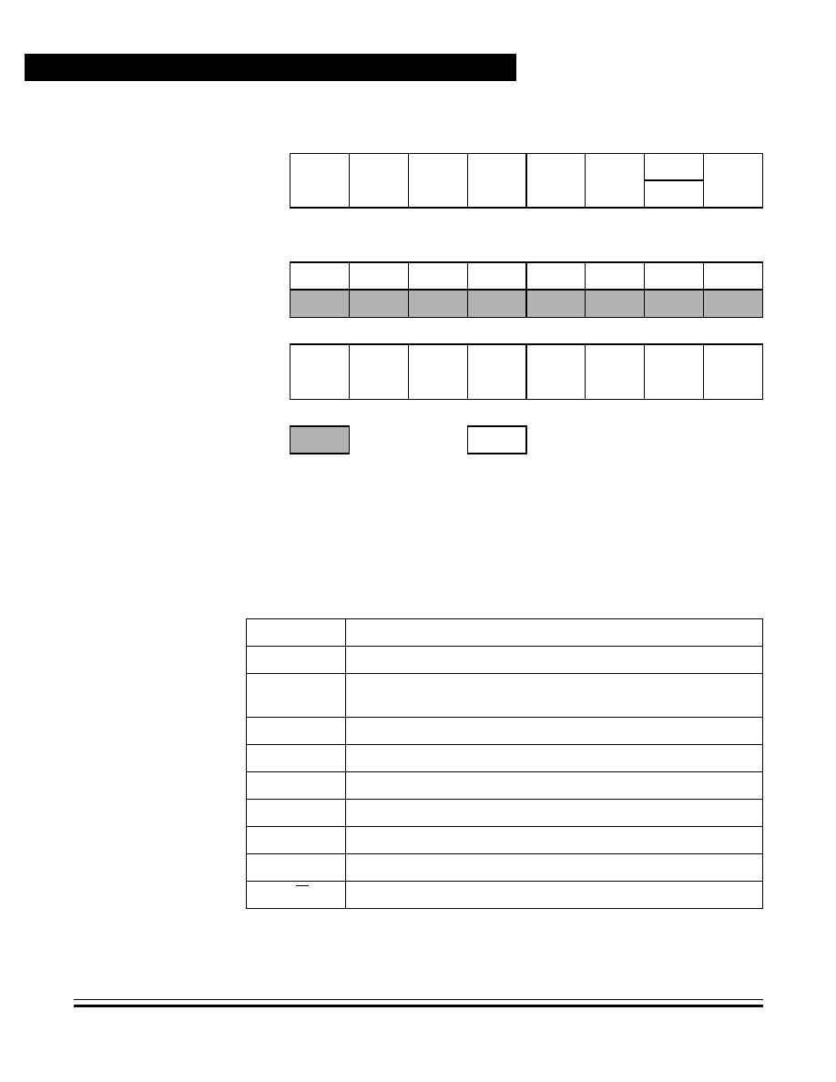
System Integration Module (SIM)
Advance Information
MC68HC908RK2
--
Rev. 4.0
82
System Integration Module (SIM)
MOTOROLA
Table 6-1
shows the internal signal names used in this section.
Addr.
Register Name
Bit 7
6
5
4
3
2
1
Bit 0
$FE00
SIM Break Status Register
(SBSR)
See page 97.
Read:
R
R
R
R
R
R
SBSW
R
Write:
See Note
Reset:
0
Note: Writing a logic 0 clears SBSW
$FE01
SIM Reset Status Register
(SRSR)
See page 98.
Read:
POR
PIN
COP
ILOP
ILAD
0
LVI
0
Write:
POR:
1
X
X
X
X
X
X
X
$FE02
SIM Break Flag Control
Register (SBFCR)
See page 99.
Read:
BCFE
R
R
R
R
R
R
R
Write:
Reset:
0
0
0
0
0
0
0
0
= Unimplemented
R
= Reserved
X = Indeterminate
Figure 6-2. SIM I/O Register Summary
Table 6-1. Signal Name Conventions
Signal Name
Description
CGMXCLK
Selected clock source from internal clock generator module (ICG)
CGMOUT
Clock output from ICG module
Bus clock = CGMOUT divided by two
ICLK
Output from internal clock generator
ECLK
External clock source
IAB
Internal address bus
IDB
internal data bus
PORRST
Signal from the power-on reset module to the SIM
IRST
Internal reset signal
R/W
Read/write signal
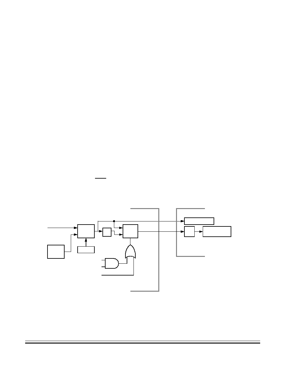
System Integration Module (SIM)
SIM Bus Clock Control and Generation
MC68HC908RK2
--
Rev. 4.0
Advance Information
MOTOROLA
System Integration Module (SIM)
83
6.3 SIM Bus Clock Control and Generation
The bus clock generator provides system clock signals for the CPU and
peripherals on the MCU. The system clocks are generated from an
incoming clock, CGMOUT, as shown in
Figure 6-3
. This clock can come
from either an external oscillator or from the internal clock generator
(ICG) module.
6.3.1 Bus Timing
In user mode, the internal bus frequency is either the crystal oscillator
output (ECLK) divided by four or the ICG output (ICLK) divided by four.
6.3.2 Clock Startup from POR or LVI Reset
When the power-on reset (POR) module or the low-voltage inhibit (LVI)
module generates a reset, the clocks to the CPU and peripherals are
inactive and held in an inactive phase until after 4096 CGMXCLK cycles.
The RST pin is driven low by the SIM during this entire period. The bus
clocks start upon completion of the timeout.
Figure 6-3. ICG Clock Signals
ICG
CGMXCLK
˜
2
BUS CLOCK
GENERATORS
SIM
ICG
SIM COUNTER
PTB3
MONITOR MODE
CLOCK
SELECT
CIRCUIT
ICLK
CS
˜
2
A
B S*
CGMOUT
*When S = 1,
CGMOUT = B
USER MODE
Generator
ECLK

System Integration Module (SIM)
Advance Information
MC68HC908RK2
--
Rev. 4.0
84
System Integration Module (SIM)
MOTOROLA
6.3.3 Clocks in Stop Mode and Wait Mode
Upon exit from stop mode by an interrupt, break, or reset, the SIM allows
CGMXCLK to clock the SIM counter. The CPU and peripheral clocks do
not become active until after the stop delay timeout. This timeout is
selectable as 4096 or 32 CGMXCLK cycles. (See
6.7.2 Stop Mode
.)
In wait mode, the CPU clocks are inactive. Refer to the wait mode
subsection of each module to see if the module is active or inactive in
wait mode. Some modules can be programmed to be active in wait
mode.
6.4 Reset and System Initialization
The MCU has these reset sources:
∑
Power-on reset module (POR)
∑
External Reset Pin (RST)
∑
Computer operating properly module (COP)
∑
Low-voltage inhibit module (LVI)
∑
Illegal opcode
∑
Illegal address
All of these resets produce the vector $FFFE≠FFFF ($FEFE≠FEFF in
monitor mode) and assert the internal reset signal (IRST). IRST causes
all registers to be returned to their default values and all modules to be
returned to their reset states.
An internal reset clears the SIM counter (see
6.5 SIM Counter
), but an
external reset does not. Each of the resets sets a corresponding bit in
the SIM reset status register (SRSR). (See
6.8 SIM Registers
.)
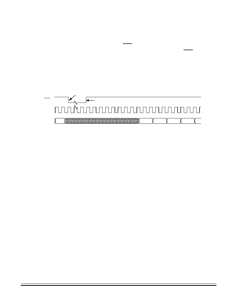
System Integration Module (SIM)
Reset and System Initialization
MC68HC908RK2
--
Rev. 4.0
Advance Information
MOTOROLA
System Integration Module (SIM)
85
6.4.1 External Pin Reset
Pulling the asynchronous RST pin low halts all processing. The PIN bit
of the SIM reset status register (SRSR) is set as long as RST is held low
for a minimum of 67 CGMXCLK cycles, assuming that neither the POR
nor the LVI was the source of the reset.
Figure 6-4
shows the relative timing of an external reset recovery.
Figure 6-4. External Reset Recovery Timing
IAB
PC
VECT H VECT L
CGMOUT
PULLED LOW EXTERNAL
RST
PULLED HIGH EXTERNAL
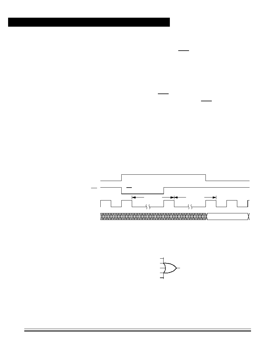
System Integration Module (SIM)
Advance Information
MC68HC908RK2
--
Rev. 4.0
86
System Integration Module (SIM)
MOTOROLA
6.4.2 Active Resets from Internal Sources
All internal reset sources actively pull the RST pin low for 32 CGMXCLK
cycles to allow resetting of external peripherals. The internal reset signal
IRST continues to be asserted for an additional 32 cycles.
(See
Figure 6-5
.) An internal reset can be caused by an illegal address,
illegal opcode, COP timeout, LVI, or POR. (See
Figure 6-6
.) Note that
for LVI or POR resets, the SIM cycles through 4096 CGMXCLK cycles
during which the SIM forces the RST pin low. The internal reset signal
then follows the sequence from the falling edge of RST shown in
Figure 6-5
.
The COP reset is asynchronous to the bus clock.
The active reset feature allows the part to issue a reset to peripherals
and other chips within a system built around the MCU.
Figure 6-5. Internal Reset Timing
Figure 6-6. Sources of Internal Reset
IRST
RST
RST PULLED LOW BY MCU
IAB
32 CYCLES
32 CYCLES
VECTOR HIGH
CGMXCLK
ILLEGAL ADDRESS RST
ILLEGAL OPCODE RST
COPRST
LVI
POR
INTERNAL RESET
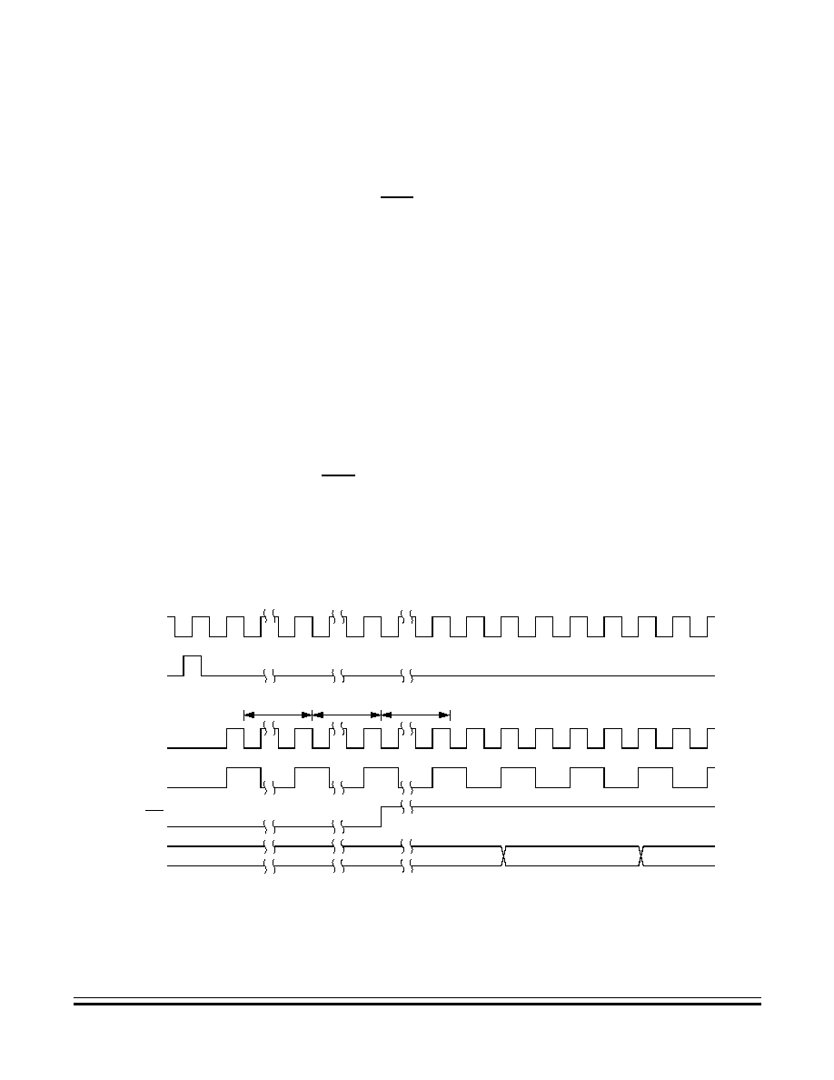
System Integration Module (SIM)
Reset and System Initialization
MC68HC908RK2
--
Rev. 4.0
Advance Information
MOTOROLA
System Integration Module (SIM)
87
6.4.2.1 Power-On Reset
When power is first applied to the MCU, the power-on reset module
(POR) generates a pulse to indicate that power-on has occurred. The
external reset pin (RST) is held low while the SIM counter counts out
4096 CGMXCLK cycles. Another 64 CGMXCLK cycles later, the CPU
and memories are released from reset to allow the reset vector
sequence to occur.
At power-on, these events occur:
∑
A POR pulse is generated.
∑
The internal reset signal is asserted.
∑
The SIM enables CGMOUT.
∑
Internal clocks to the CPU and modules are held inactive for 4096
CGMXCLK cycles to allow stabilization of the oscillator.
∑
The RST pin is driven low during the oscillator stabilization time.
∑
The POR bit of the SIM reset status register (SRSR) is set and all
other bits in the register are cleared.
Figure 6-7. POR Recovery
PORRST
OSC1
CGMXCLK
CGMOUT
RST
IAB
4096
CYCLES
32
CYCLES
32
CYCLES
$FFFE
$FFFF

System Integration Module (SIM)
Advance Information
MC68HC908RK2
--
Rev. 4.0
88
System Integration Module (SIM)
MOTOROLA
6.4.2.2 Computer Operating Properly (COP) Reset
The overflow of the COP counter causes an internal reset and sets the
COP bit in the SIM reset status register (SRSR) if the COPD bit in the
CONFIG register is at logic 0. (See
Section 11. Computer Operating
Properly Module (COP)
.)
6.4.2.3 Illegal Opcode Reset
The SIM decodes signals from the CPU to detect illegal instructions. An
illegal instruction sets the ILOP bit in the SIM reset status register
(SRSR) and causes a reset.
If the stop enable bit, STOP, in the configuration register (CONFIG) is
logic 0, the SIM treats the STOP instruction as an illegal opcode and
causes an illegal opcode reset.
6.4.2.4 Illegal Address Reset
An opcode fetch from an unmapped address generates an illegal
address reset. The SIM verifies that the CPU is fetching an opcode prior
to asserting the ILAD bit in the SIM reset status register (SRSR) and
resetting the MCU. A data fetch from an unmapped address does not
generate a reset.
6.4.2.5 Low-Voltage Inhibit (LVI) Reset
The low-voltage inhibit module (LVI) asserts its output to the SIM when
the V
DD
voltage falls to the V
LVR
voltage. The LVI bit in the SIM reset
status register (SRSR) is set and a chip reset is asserted if the LVIPWRD
and LVIRSTD bits in the CONFIG register are at logic 0. The RST pin will
be held low until the SIM counts 4096 CGMXCLK cycles after V
DD
rises
above V
LVR
+ H
LVR
. Another 64 CGMXCLK cycles later, the CPU is
released from reset to allow the reset vector sequence to occur. (See
Section 12. Low-Voltage Inhibit (LVI)
.)

System Integration Module (SIM)
SIM Counter
MC68HC908RK2
--
Rev. 4.0
Advance Information
MOTOROLA
System Integration Module (SIM)
89
6.5 SIM Counter
The SIM counter is used by the power-on reset module (POR) and in
stop mode recovery to allow the oscillator time to stabilize before
enabling the internal bus (IBUS) clocks. The SIM counter also serves as
a prescaler for the computer operating properly module (COP). The SIM
counter overflow supplies the clock for the COP module. The SIM
counter is 12 bits long and is clocked by the falling edge of CGMXCLK.
6.5.1 SIM Counter During Power-On Reset
The power-on reset module (POR) detects power applied to the MCU.
At power-on, the POR circuit asserts the signal PORRST. Once the SIM
is initialized, it enables the internal clock generation module (ICG) to
drive the bus clock state machine.
6.5.2 SIM Counter During Stop Mode Recovery
The SIM counter also is used for stop mode recovery. The STOP
instruction clears the SIM counter. After an interrupt, break, or reset, the
SIM senses the state of the short stop recovery bit, SSREC, in the
CONFIG register. If the SSREC bit is a logic 1, then the stop recovery is
reduced from the normal delay of 4096 CGMXCLK cycles down to 32
CGMXCLK cycles. This is ideal for applications using canned oscillators
that do not require long startup times from stop mode. External crystal
applications should use the full stop recovery time, that is, with SSREC
cleared.
6.5.3 SIM Counter and Reset States
External reset has no effect on the SIM counter. See
6.7.2 Stop Mode
for details. The SIM counter is free-running after all reset states. See
6.4.2 Active Resets from Internal Sources
for counter control and
internal reset recovery sequences.
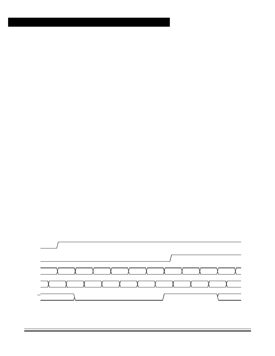
System Integration Module (SIM)
Advance Information
MC68HC908RK2
--
Rev. 4.0
90
System Integration Module (SIM)
MOTOROLA
6.6 Program Exception Control
Normal, sequential program execution can be changed in three different
ways:
1. Interrupts:
a. Maskable hardware CPU interrupts
b. Non-maskable software interrupt instruction (SWI)
2. Reset
3. Break interrupts
6.6.1 Interrupts
At the beginning of an interrupt, the CPU saves the CPU register
contents on the stack and sets the interrupt mask (I bit) to prevent
additional interrupts. At the end of an interrupt, the RTI instruction
recovers the CPU register contents from the stack so that normal
processing can resume.
Figure 6-8
shows interrupt entry timing.
Figure 6-10
shows interrupt recovery timing.
Interrupts are latched, and arbitration is performed in the SIM at the start
of interrupt processing. The arbitration result is a constant that the CPU
uses to determine which vector to fetch. Once an interrupt is latched by
the SIM, no other interrupt can take precedence, regardless of priority,
until the latched interrupt is serviced (or the I bit is cleared).
(See
Figure 6-9
.)
Figure 6-8
.
Interrupt Entry
MODULE
IDB
R/W
INTERRUPT
DUMMY
SP
SP ≠ 1
SP ≠ 2
SP ≠ 3
SP ≠ 4
VECT H
VECT L
START ADDR
IAB
DUMMY
PC ≠ 1[7:0]
PC ≠ 1[15:8]
X
A
CCR
V DATA H
V DATA L
OPCODE
I BIT

System Integration Module (SIM)
Program Exception Control
MC68HC908RK2
--
Rev. 4.0
Advance Information
MOTOROLA
System Integration Module (SIM)
91
Figure 6-9. Interrupt Processing
NO
NO
NO
YES
NO
NO
YES
YES
AS MANY INTERRUPTS
I BIT SET?
FROM RESET
BREAK INTERRUPT?
I BIT SET?
IRQ
INTERRUPT?
SWI
INSTRUCTION?
RTI
INSTRUCTION?
FETCH NEXT
INSTRUCTION
UNSTACK CPU REGISTERS
STACK CPU REGISTERS
SET I BIT
LOAD PC WITH INTERRUPT VECTOR
EXECUTE INSTRUCTION
YES
YES
AS EXIST ON CHIP
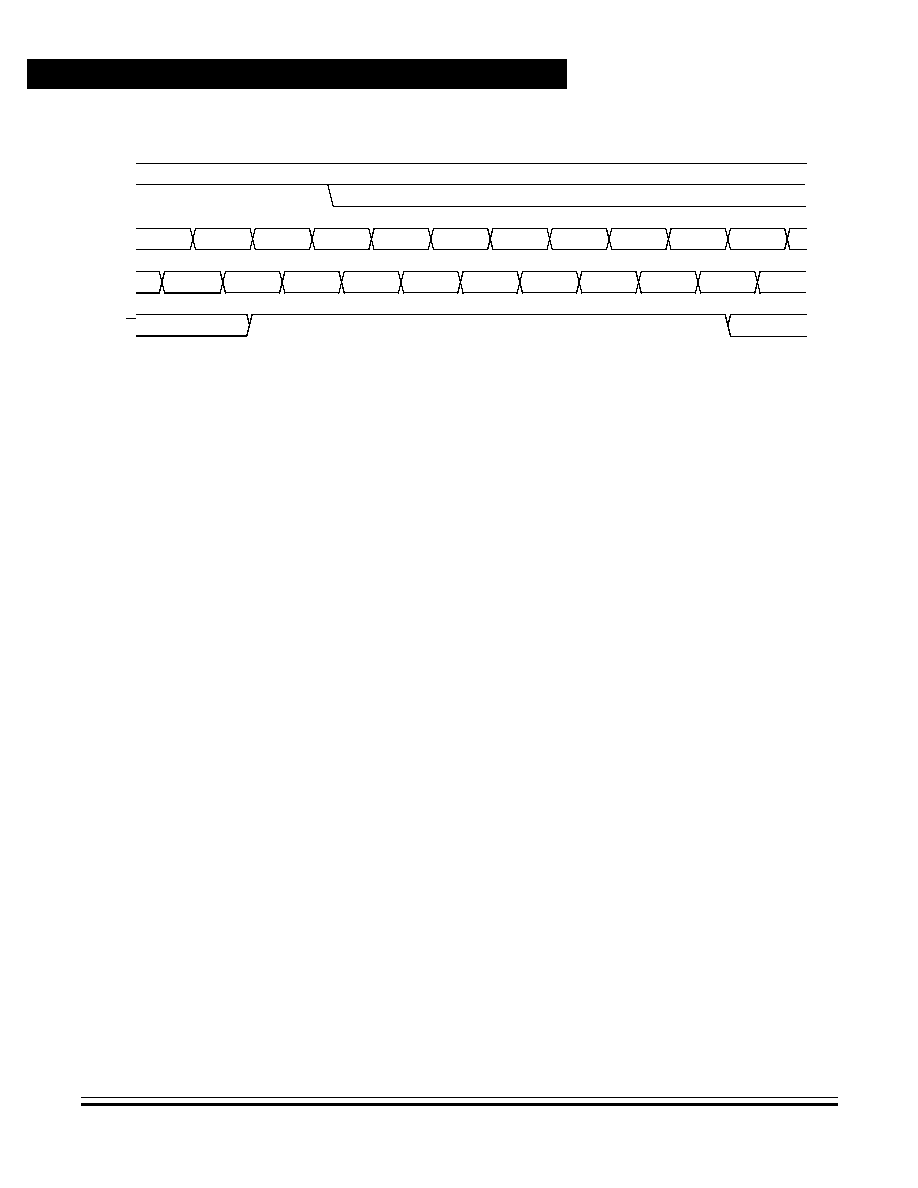
System Integration Module (SIM)
Advance Information
MC68HC908RK2
--
Rev. 4.0
92
System Integration Module (SIM)
MOTOROLA
Figure 6-10. Interrupt Recovery
6.6.1.1 Hardware Interrupts
A hardware interrupt does not stop the current instruction. Processing of
a hardware interrupt begins after completion of the current instruction.
When the current instruction is complete, the SIM checks all pending
hardware interrupts. If interrupts are not masked (I bit clear in the
condition code register), and if the corresponding interrupt enable bit is
set, the SIM proceeds with interrupt processing; otherwise, the next
instruction is fetched and executed.
If more than one interrupt is pending at the end of an instruction
execution, the highest priority interrupt is serviced first.
Figure 6-11
demonstrates what happens when two interrupts are pending. If an
interrupt is pending upon exit from the original interrupt service routine,
the pending interrupt is serviced before the LDA instruction is executed.
The LDA opcode is prefetched by both the INT1 and INT2 RTI
instructions. However, in the case of the INT1 RTI prefetch, this is a
redundant operation.
NOTE:
To maintain compatibility with the M68HC05, M6805, and M146805
Families the H register is not pushed on the stack during interrupt entry.
If the interrupt service routine modifies the H register or uses the indexed
addressing mode, software should save the H register and then restore
it prior to exiting the routine.
MODULE
IDB
R/W
INTERRUPT
SP ≠ 4
SP ≠ 3
SP ≠ 2
SP ≠ 1
SP
PC
PC + 1
IAB
CCR
A
X
PC ≠ 1 [15:8]
PC ≠ 1 [7:0]
OPCODE
OPERAND
I BIT
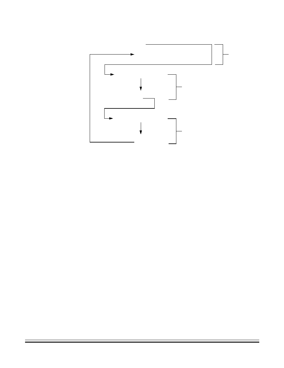
System Integration Module (SIM)
Program Exception Control
MC68HC908RK2
--
Rev. 4.0
Advance Information
MOTOROLA
System Integration Module (SIM)
93
Figure 6-11
.
Interrupt Recognition Example
6.6.1.2 SWI Instruction
The SWI instruction is a non-maskable instruction that causes an
interrupt regardless of the state of the interrupt mask (I bit) in the
condition code register.
NOTE:
A software interrupt pushes PC onto the stack. A software interrupt does
not push PC ≠ 1, as a hardware interrupt does.
6.6.2 Reset
All reset sources always have higher priority than interrupts and cannot
be arbitrated.
6.6.3 Break Interrupts
The break module can stop normal program flow at a software-
programmable break point by asserting its break interrupt output. (See
Section 7. Break Module (BRK)
.) The SIM puts the CPU into the break
state by forcing it to the SWI vector location. Refer to the break interrupt
CLI
LDA
INT1
PULH
RTI
INT2
BACKGROUND
#$FF
PSHH
INT1 INTERRUPT SERVICE ROUTINE
PULH
RTI
PSHH
INT2 INTERRUPT SERVICE ROUTINE
ROUTINE

System Integration Module (SIM)
Advance Information
MC68HC908RK2
--
Rev. 4.0
94
System Integration Module (SIM)
MOTOROLA
subsection of each module to see how each module is affected by the
break state.
6.6.4 Status Flag Protection in Break Mode
The SIM controls whether status flags contained in other modules can
be cleared during break mode. The user can select whether flags are
protected from being cleared by properly initializing the break clear flag
enable bit (BCFE) in the break flag control register (BFCR).
Protecting flags in break mode ensures that set flags will not be cleared
while in break mode. This protection allows registers to be freely read
and written during break mode without losing status flag information.
Setting the BCFE bit enables the clearing mechanisms. Once cleared in
break mode, a flag remains cleared even when break mode is exited.
Status flags with a 2-step clearing mechanism -- for example, a read of
one register followed by the read or write of another -- are protected,
even when the first step is accomplished prior to entering break mode.
Upon leaving break mode, execution of the second step will clear the flag
as normal.
6.7 Low-Power Modes
Executing the WAIT or STOP instruction puts the MCU in a low power-
consumption mode for standby situations. The SIM holds the CPU in a
non-clocked state. The operation of each of these modes is described
here. Both STOP and WAIT clear the interrupt mask (I) in the condition
code register, allowing interrupts to occur.
6.7.1 Wait Mode
In wait mode, the CPU clocks are inactive while one set of peripheral
clocks continues to run.
Figure 6-12
shows the timing for wait mode
entry.
A module that is active during wait mode can wake up the CPU with an
interrupt if the interrupt is enabled. Stacking for the interrupt begins one
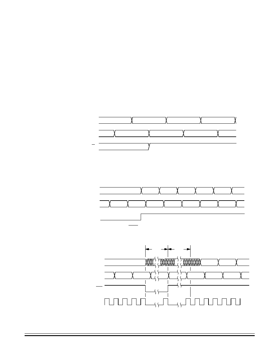
System Integration Module (SIM)
Low-Power Modes
MC68HC908RK2
--
Rev. 4.0
Advance Information
MOTOROLA
System Integration Module (SIM)
95
cycle after the WAIT instruction during which the interrupt occurred.
Refer to the wait mode subsection of each module to see if the module
is active or inactive in wait mode. Some modules can be programmed to
be active in wait mode.
Wait mode can also be exited by a reset or break. A break interrupt
during wait mode sets the SIM break stop/wait bit, SBSW, in the SIM
break status register (SBSR). If the COP disable bit, COPD, in the mask
option register is logic 0, then the computer operating properly module
(COP) is enabled and remains active in wait mode.
Figure 6-12. Wait Mode Entry Timing
Figure 6-13
and
Figure 6-14
show the timing for WAIT recovery.
Figure 6-13. Wait Recovery from Interrupt or Break
Figure 6-14. Wait Recovery from Internal Reset
WAIT ADDR + 1
SAME
SAME
IAB
IDB
PREVIOUS DATA
NEXT OPCODE
SAME
WAIT ADDR
SAME
R/W
Note: Previous data can be operand data or the WAIT opcode, depending on the last instruction.
$6E0C
$6E0B
$00FF
$00FE
$00FD
$00FC
$A6
$A6
$01
$0B
$6E
$A6
IAB
IDB
EXITSTOPWAIT
Note: EXITSTOPWAIT =
RST
pin or CPU interrupt or break interrupt
IAB
IDB
RST
$A6
$A6
$6E0B
RST VCT H
RST VCT L
$A6
CGMXCLK
32
CYCLES
32
CYCLES
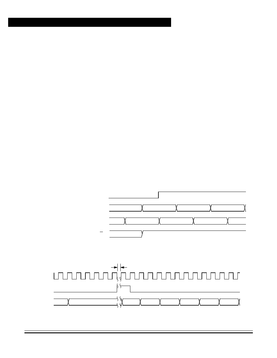
System Integration Module (SIM)
Advance Information
MC68HC908RK2
--
Rev. 4.0
96
System Integration Module (SIM)
MOTOROLA
6.7.2 Stop Mode
In stop mode, the SIM counter is reset and the system clocks are
disabled. An interrupt request from a module can cause an exit from stop
mode. Stacking for interrupts begins after the selected stop recovery
time has elapsed. Reset or break also causes an exit from stop mode.
The SIM disables the clock generator module outputs (CGMOUT and
CGMXCLK) in stop mode, stopping the CPU and peripherals. Stop
recovery time is selectable using the SSREC bit in the CONFIG register.
If SSREC is set, stop recovery is reduced from the normal delay of 4096
CGMXCLK cycles down to 32. This is ideal for applications using canned
oscillators that do not require long startup times from stop mode.
NOTE:
External crystal applications should use the full stop recovery time by
clearing the SSREC bit.
A break interrupt during stop mode sets the SIM break stop/wait bit
(SBSW) in the SIM break status register (SBSR).
The SIM counter is held in reset from the execution of the STOP
instruction until the beginning of stop recovery. It is then used to time the
recovery period.
Figure 6-15
shows stop mode entry timing.
Figure 6-15. Stop Mode Entry Timing
Figure 6-16. Stop Mode Recovery from Interrupt or Break
STOP ADDR + 1
SAME
SAME
IAB
IDB
PREVIOUS DATA
NEXT OPCODE
SAME
STOP ADDR
SAME
R/W
CPUSTOP
Note: Previous data can be operand data or the STOP opcode, depending on the last
instruction
.
CGMXCLK
INT/BREAK
IAB
STOP + 2
STOP + 2
SP
SP ≠ 1
SP ≠ 2
SP ≠ 3
STOP +1
STOP RECOVERY PERIOD

System Integration Module (SIM)
SIM Registers
MC68HC908RK2
--
Rev. 4.0
Advance Information
MOTOROLA
System Integration Module (SIM)
97
6.8 SIM Registers
The SIM has three memory mapped registers:
∑
SIM break status register, SBSR
∑
SIM reset status register, SRSR
∑
SIM break flag control register, SBFCR
6.8.1 SIM Break Status Register
The SIM break status register (SBSR) contains a flag to indicate that a
break caused an exit from stop or wait mode.
SBSW -- SIM Break Stop/Wait Bit
This status bit is useful in applications requiring a return to wait or stop
mode after exiting from a break interrupt. Clear SBSW by writing a
logic 0 to it. Reset clears SBSW.
1 = Stop mode or wait mode was exited by break interrupt.
0 = Stop mode or wait mode was not exited by break interrupt.
SBSW can be read within the break state SWI routine. The user can
modify the return address on the stack by subtracting one from it.
(See code example.) Writing 0 to the SBSW bit clears it.
;This code works if the H register has been pushed onto the stack in the break
;service routine software. This code should be executed at the end of the
;break service routine software.
HIBYTE
EQU
5
LOBYTE
EQU
6
;
If not SBSW, do RTI
BRCLR
SBSW, SBSR, RETURN
;See if wait mode or stop mode was exited
;by break.
TST
LOBYTE,SP
;If RETURNLO is not zero,
BNE
DOLO
;then just decrement low byte.
DEC
HIBYTE,SP
;Else deal with high byte, too.
DOLO
DEC
LOBYTE,SP
;Point to WAIT/STOP opcode.
RETURN
PULH
RTI
;Restore H register.
Address:
$FE00
Bit 7
6
5
4
3
2
1
Bit 0
Read:
R
R
R
R
R
R
SBSW
R
Write:
See Note
Reset:
0
R
= Reserved
Note: Writing a logic 0 clears SBSW.
Figure 6-17. SIM Break Status Register (SBSR)
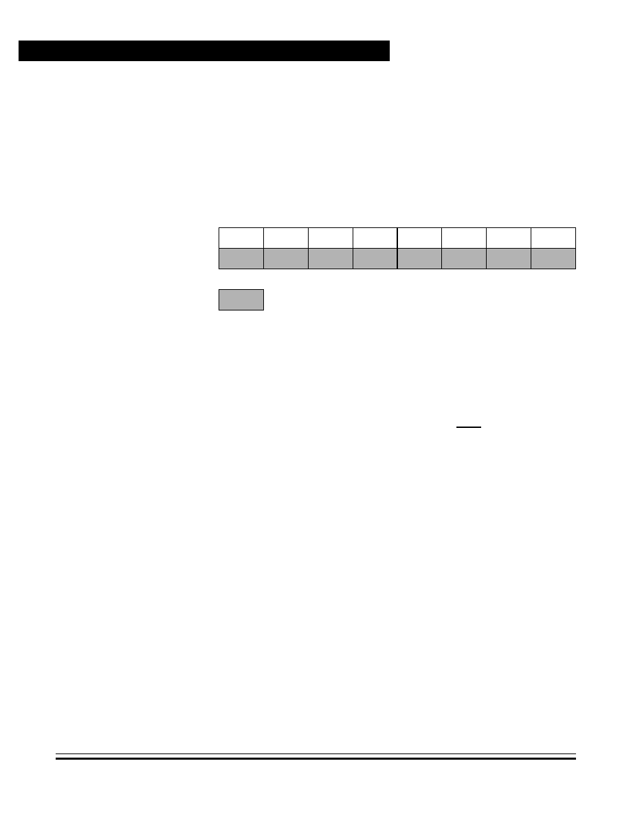
System Integration Module (SIM)
Advance Information
MC68HC908RK2
--
Rev. 4.0
98
System Integration Module (SIM)
MOTOROLA
6.8.2 SIM Reset Status Register
This register contains six flags that show the source of the last reset. The
status register will clear automatically after reading it. A power-on reset
sets the POR bit.
POR -- Power-On Reset Bit
1 = Last reset caused by POR circuit
0 = Read of SRSR
PIN -- External Reset Bit
1 = Last reset caused by external reset pin (RST)
0 = Read of SRSR
COP -- Computer Operating Properly Reset Bit
1 = Last reset caused by COP counter
0 = Read of SRSR
ILOP -- Illegal Opcode Reset Bit
1 = Last reset caused by an illegal opcode
0 = Read of SRSR
ILAD -- Illegal Address Reset Bit (opcode fetches only)
1 = Last reset caused by an opcode fetch from an illegal address
0 = Read of SRSR
LVI -- Low-Voltage Inhibit Reset Bit
1 = Last reset was caused by the LVI circuit
0 = Read of SRSR
Address:
$FE01
Bit 7
6
5
4
3
2
1
Bit 0
Read:
POR
PIN
COP
ILOP
ILAD
0
LVI
0
Write:
POR:
1
X
X
X
X
X
X
X
= Unimplemented
X = Indeterminate
Figure 6-18. SIM Reset Status Register (SRSR)

System Integration Module (SIM)
SIM Registers
MC68HC908RK2
--
Rev. 4.0
Advance Information
MOTOROLA
System Integration Module (SIM)
99
6.8.3 SIM Break Flag Control Register
The SIM break control register contains a bit that enables software to
clear status bits while the MCU is in a break state.
BCFE -- Break Clear Flag Enable Bit
This read/write bit enables software to clear status bits by accessing
status registers while the MCU is in a break state. To clear status bits
during the break state, the BCFE bit must be set.
1 = Status bits clearable during break
0 = Status bits not clearable during break
Address:
$FE02
Bit 7
6
5
4
3
2
1
Bit 0
Read:
BCFE
R
R
R
R
R
R
R
Write:
Reset:
0
0
0
0
0
0
0
0
R
= Reserved
Figure 6-19. SIM Break Flag Control Register (SBFCR)

System Integration Module (SIM)
Advance Information
MC68HC908RK2
--
Rev. 4.0
100
System Integration Module (SIM)
MOTOROLA

MC68HC908RK2
--
Rev. 4.0
Advance Information
MOTOROLA
Break Module (BRK)
101
Advance Information -- MC68HC908RK2
Section 7. Break Module (BRK)
7.1 Contents
7.2
Introduction . . . . . . . . . . . . . . . . . . . . . . . . . . . . . . . . . . . . . . . 101
7.3
Features . . . . . . . . . . . . . . . . . . . . . . . . . . . . . . . . . . . . . . . . . 101
7.4
Functional Description . . . . . . . . . . . . . . . . . . . . . . . . . . . . . . 102
7.4.1
Flag Protection During Break Interrupts . . . . . . . . . . . . . . . 103
7.4.2
CPU During Break Interrupts . . . . . . . . . . . . . . . . . . . . . . .103
7.4.3
TIM During Break Interrupts . . . . . . . . . . . . . . . . . . . . . . . . 104
7.4.4
COP During Break Interrupts . . . . . . . . . . . . . . . . . . . . . . .104
7.5
Low-Power Modes . . . . . . . . . . . . . . . . . . . . . . . . . . . . . . . . . 104
7.5.1
Wait Mode . . . . . . . . . . . . . . . . . . . . . . . . . . . . . . . . . . . . .104
7.5.2
Stop Mode . . . . . . . . . . . . . . . . . . . . . . . . . . . . . . . . . . . . .104
7.6
Break Module Registers . . . . . . . . . . . . . . . . . . . . . . . . . . . . . 104
7.6.1
Break Status and Control Register . . . . . . . . . . . . . . . . . . .105
7.6.2
Break Address Registers . . . . . . . . . . . . . . . . . . . . . . . . . . 106
7.2 Introduction
The break module can generate a break interrupt that stops normal
program flow at a defined address to enter a background program.
7.3 Features
Features of the break module (BRK) include:
∑
Accessible input/output (I/O) registers during break interrupts
∑
CPU-generated break interrupts
∑
Software-generated break interrupts
∑
COP disabling during break interrupts

Break Module (BRK)
Advance Information
MC68HC908RK2
--
Rev. 4.0
102
Break Module (BRK)
MOTOROLA
7.4 Functional Description
When the internal address bus matches the value written in the break
address registers, the break module issues a breakpoint signal to the
CPU. The CPU then loads the instruction register with a software
interrupt instruction (SWI) after completion of the current CPU
instruction. The program counter vectors to $FFFC and $FFFD ($FEFC
and $FEFD in monitor mode).
These events can cause a break interrupt to occur:
∑
A CPU-generated address (the address in the program counter)
matches the contents of the break address registers.
∑
Software writes a logic 1 to the BRKA bit in the break status and
control register.
When a CPU-generated address matches the contents of the break
address registers, the break interrupt begins after the CPU completes its
current instruction. A return-from-interrupt instruction (RTI) in the break
routine ends the break interrupt and returns the MCU to normal
operation.
Figure 7-1
shows the structure of the break module.
Figure 7-1. Break Module Block Diagram
IAB[15:8]
IAB[7:0]
8-BIT COMPARATOR
8-BIT COMPARATOR
CONTROL
BREAK ADDRESS REGISTER LOW
BREAK ADDRESS REGISTER HIGH
IAB[15:0]
BREAK
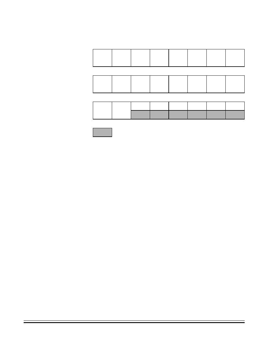
Break Module (BRK)
Functional Description
MC68HC908RK2
--
Rev. 4.0
Advance Information
MOTOROLA
Break Module (BRK)
103
7.4.1 Flag Protection During Break Interrupts
The system integration module (SIM) controls whether module status
bits can be cleared during the break state. The BCFE bit in the SIM break
flag control register (BFCR) enables software to clear status bits during
the break state. (See
6.8.3 SIM Break Flag Control Register
and the
Break Interrupts subsection for each module.)
7.4.2 CPU During Break Interrupts
The CPU starts a break interrupt by:
∑
Loading the instruction register with the SWI instruction
∑
Loading the program counter with $FFFC and $FFFD ($FEFC and
$FEFD in monitor mode)
The break interrupt begins after completion of the CPU instruction in
progress. If the break address register match occurs on the last cycle of
a CPU instruction, the break interrupt begins immediately.
Addr.
Register Name
Bit 7
6
5
4
3
2
1
Bit 0
$FE0C
Break Address Register
High (BRKH)
See page 106.
Read:
Bit 15
14
13
12
11
10
9
Bit 8
Write:
Reset:
0
0
0
0
0
0
0
0
$FE0D
Break Address Register
Low (BRKL)
See page 106.
Read:
Bit 7
6
5
4
3
2
1
Bit 0
Write:
Reset:
0
0
0
0
0
0
0
0
$FE0E
Break Status and Control
Register (BSCR)
See page 105.
Read:
BRKE
BRKA
0
0
0
0
0
0
Write:
Reset:
0
0
0
0
0
0
0
0
= Unimplemented
Figure 7-2. I/O Register Summary

Break Module (BRK)
Advance Information
MC68HC908RK2
--
Rev. 4.0
104
Break Module (BRK)
MOTOROLA
7.4.3 TIM During Break Interrupts
A break interrupt stops the timer counter.
7.4.4 COP During Break Interrupts
The COP is disabled during a break interrupt when V
HI
is present on the
RST pin.
7.5 Low-Power Modes
The WAIT and STOP instructions put the MCU in low power-
consumption standby modes.
7.5.1 Wait Mode
If enabled, the break module is active in wait mode.
7.5.2 Stop Mode
The break module is inactive in stop mode. The STOP instruction does
not affect break module register states.
7.6 Break Module Registers
These registers control and monitor operation of the break module:
∑
Break status and control register, BSCR
∑
Break address register high, BRKH
∑
Break address register low, BRKL

Break Module (BRK)
Break Module Registers
MC68HC908RK2
--
Rev. 4.0
Advance Information
MOTOROLA
Break Module (BRK)
105
7.6.1 Break Status and Control Register
The break status and control register (BSCR) contains break module
enable and status bits.
BRKE -- Break Enable Bit
This read/write bit enables breaks on break address register matches.
Clear BRKE by writing a logic 0 to bit 7. Reset clears the BRKE bit.
1 = Breaks enabled on 16-bit address match
0 = Breaks disabled on 16-bit address match
BRKA -- Break Active Bit
This read/write status and control bit is set when a break address
match occurs. Writing a logic 1 to BRKA generates a break interrupt.
Clear BRKA by writing a logic 0 to it before exiting the break routine.
1 = Break address match
0 = No break address match
Address:
$FE0E
Bit 7
6
5
4
3
2
1
Bit 0
Read:
BRKE
BRKA
0
0
0
0
0
0
Write:
Reset:
0
0
0
0
0
0
0
0
= Unimplemented
Figure 7-3. Break Status and Control Register (BSCR)

Break Module (BRK)
Advance Information
MC68HC908RK2
--
Rev. 4.0
106
Break Module (BRK)
MOTOROLA
7.6.2 Break Address Registers
The break address registers contain the high and low bytes of the
desired breakpoint address. Reset clears the break address registers.
Register Name and Address: BRKH--$FE0C
Bit 7
6
5
4
3
2
1
Bit 0
Read:
Bit 15
14
13
12
11
10
9
Bit 8
Write:
Reset:
0
0
0
0
0
0
0
0
Register Name and Address: BRKL--$FE0D
Bit 7
6
5
4
3
2
1
Bit 0
Read:
Bit 7
6
5
4
3
2
1
Bit 0
Write:
Reset:
0
0
0
0
0
0
0
0
Figure 7-4. Break Address Registers (BRKH and BRKL)

MC68HC908RK2
--
Rev. 4.0
Advance Information
MOTOROLA
Internal Clock Generator Module (ICG)
107
Advance Information -- MC68HC908RK2
Section 8. Internal Clock Generator Module (ICG)
8.1 Contents
8.2
Introduction . . . . . . . . . . . . . . . . . . . . . . . . . . . . . . . . . . . . . . . 108
8.3
Features . . . . . . . . . . . . . . . . . . . . . . . . . . . . . . . . . . . . . . . . . 108
8.4
Functional Description . . . . . . . . . . . . . . . . . . . . . . . . . . . . . . 109
8.4.1
Clock Enable Circuit . . . . . . . . . . . . . . . . . . . . . . . . . . . . . . 109
8.4.2
Internal Clock Generator . . . . . . . . . . . . . . . . . . . . . . . . . . 111
8.4.2.1
Digitally Controlled Oscillator . . . . . . . . . . . . . . . . . . . . . 112
8.4.2.2
Modulo N Divider . . . . . . . . . . . . . . . . . . . . . . . . . . . . . . 112
8.4.2.3
Frequency Comparator . . . . . . . . . . . . . . . . . . . . . . . . . 112
8.4.2.4
Digital Loop Filter . . . . . . . . . . . . . . . . . . . . . . . . . . . . . . 113
8.4.3
External Clock Generator . . . . . . . . . . . . . . . . . . . . . . . . . . 114
8.4.3.1
External Oscillator Amplifier . . . . . . . . . . . . . . . . . . . . . . 114
8.4.3.2
External Clock Input Path . . . . . . . . . . . . . . . . . . . . . . .115
8.4.4
Clock Monitor Circuit . . . . . . . . . . . . . . . . . . . . . . . . . . . . . 115
8.4.4.1
Clock Monitor Reference Generator . . . . . . . . . . . . . . . 116
8.4.4.2
Internal Clock Activity Detector . . . . . . . . . . . . . . . . . . . 119
8.4.4.3
External Clock Activity Detector . . . . . . . . . . . . . . . . . . .119
8.4.5
Clock Selection Circuit . . . . . . . . . . . . . . . . . . . . . . . . . . . .120
8.4.5.1
Clock Selection Switch. . . . . . . . . . . . . . . . . . . . . . . . . . 120
8.4.5.2
Clock Switching Circuit. . . . . . . . . . . . . . . . . . . . . . . . . . 121
8.5
Usage Notes . . . . . . . . . . . . . . . . . . . . . . . . . . . . . . . . . . . . . . 122
8.5.1
Switching Clock Sources . . . . . . . . . . . . . . . . . . . . . . . . . . 123
8.5.2
Enabling the Clock Monitor . . . . . . . . . . . . . . . . . . . . . . . . 124
8.5.3
Clock Monitor Interrupts . . . . . . . . . . . . . . . . . . . . . . . . . . . 125
8.5.4
Quantization Error in DCO Output . . . . . . . . . . . . . . . . . . . 125
8.5.4.1
Digitally Controlled Oscillator . . . . . . . . . . . . . . . . . . . . . 126
8.5.4.2
Binary Weighted Divider . . . . . . . . . . . . . . . . . . . . . . . . 126
8.5.4.3
Variable-Delay Ring Oscillator . . . . . . . . . . . . . . . . . . . . 127
8.5.4.4
Ring Oscillator Fine-Adjust Circuit . . . . . . . . . . . . . . . . . 127
8.5.5
Switching Internal Clock Frequencies . . . . . . . . . . . . . . . . 128

Internal Clock Generator Module (ICG)
Advance Information
MC68HC908RK2
--
Rev. 4.0
108
Internal Clock Generator Module (ICG)
MOTOROLA
8.5.6
Nominal Frequency Settling Time . . . . . . . . . . . . . . . . . . . 129
8.5.6.1
Settling to Within 15 Percent . . . . . . . . . . . . . . . . . . . . . 129
8.5.6.2
Settling to Within 5 Percent . . . . . . . . . . . . . . . . . . . . . . 130
8.5.6.3
Total Settling Time . . . . . . . . . . . . . . . . . . . . . . . . . . . . . 130
8.5.7
Improving Settling Time . . . . . . . . . . . . . . . . . . . . . . . . . . . 131
8.5.8
Trimming Frequency on the Internal Clock Generator . . . . 133
8.6
Low-Power Modes . . . . . . . . . . . . . . . . . . . . . . . . . . . . . . . . . 135
8.6.1
Wait Mode . . . . . . . . . . . . . . . . . . . . . . . . . . . . . . . . . . . . .135
8.6.2
Stop Mode . . . . . . . . . . . . . . . . . . . . . . . . . . . . . . . . . . . . .135
8.7
Configuration Register Option . . . . . . . . . . . . . . . . . . . . . . . . 135
8.7.1
EXTSLOW . . . . . . . . . . . . . . . . . . . . . . . . . . . . . . . . . . . . .136
8.8
I/O Registers. . . . . . . . . . . . . . . . . . . . . . . . . . . . . . . . . . . . . . 136
8.8.1
ICG Control Register . . . . . . . . . . . . . . . . . . . . . . . . . . . . . 139
8.8.2
ICG Multiplier Register . . . . . . . . . . . . . . . . . . . . . . . . . . . .141
8.8.3
ICG Trim Register . . . . . . . . . . . . . . . . . . . . . . . . . . . . . . . 142
8.8.4
ICG DCO Divider Register . . . . . . . . . . . . . . . . . . . . . . . . . 143
8.8.5
ICG DCO Stage Register . . . . . . . . . . . . . . . . . . . . . . . . . . 144
8.2 Introduction
The Internal Clock Generator Module (ICG) is used to create a stable
clock source for the microcontroller without using any external
components. The ICG generates the Oscillator Output Clock
(CGMXCLK), which is used by the COP, LVI, and other modules. The
ICG also generates the clock generator output (CGMOUT), which is fed
to the system integration module (SIM) to create the bus clocks. The bus
frequency will be one-fourth the frequency of CGMXCLK and one-half
the frequency of CGMOUT.
8.3 Features
The ICG has these features:
∑
External clock generator, either 1-pin external source or 2-pin
crystal
∑
Internal clock generator with programmable frequency output in
integer multiples of a nominal frequency (307.2 kHz
±
25 percent)

Internal Clock Generator Module (ICG)
Functional Description
MC68HC908RK2
--
Rev. 4.0
Advance Information
MOTOROLA
Internal Clock Generator Module (ICG)
109
∑
Frequency adjust (trim) register to improve variability to
±
2 percent
∑
Bus clock software selectable from either internal or external clock
∑
Clock monitor for both internal and external clocks
8.4 Functional Description
The ICG, shown in
Figure 8-1
, contains these major submodules:
∑
Clock enable circuit
∑
Internal clock generator
∑
External clock generator
∑
Clock monitor circuit
∑
Clock selection circuit
8.4.1 Clock Enable Circuit
The clock enable circuit is used to enable the internal clock (ICLK) or
external clock (ECLK). The clock enable circuit generates an ICG stop
(ICGSTOP) signal which stops all clocks (ICLK, ECLK, and the low-
frequency base clock, IBASE) low. ICGSTOP is set and the ICG is
disabled in stop mode.
The internal clock enable signal (ICGEN) turns on the internal clock
generator which generates ICLK. ICGEN is set (active) whenever the
ICGON bit is set and the ICGSTOP signal is clear. When ICGEN is clear,
ICLK and IBASE are both low.
The external clock enable signal (ECGEN) turns on the external clock
generator which generates ECLK. ECGEN is set (active) whenever the
ECGON bit is set and the ICGSTOP signal is clear. When ECGEN is
clear, ECLK is low.
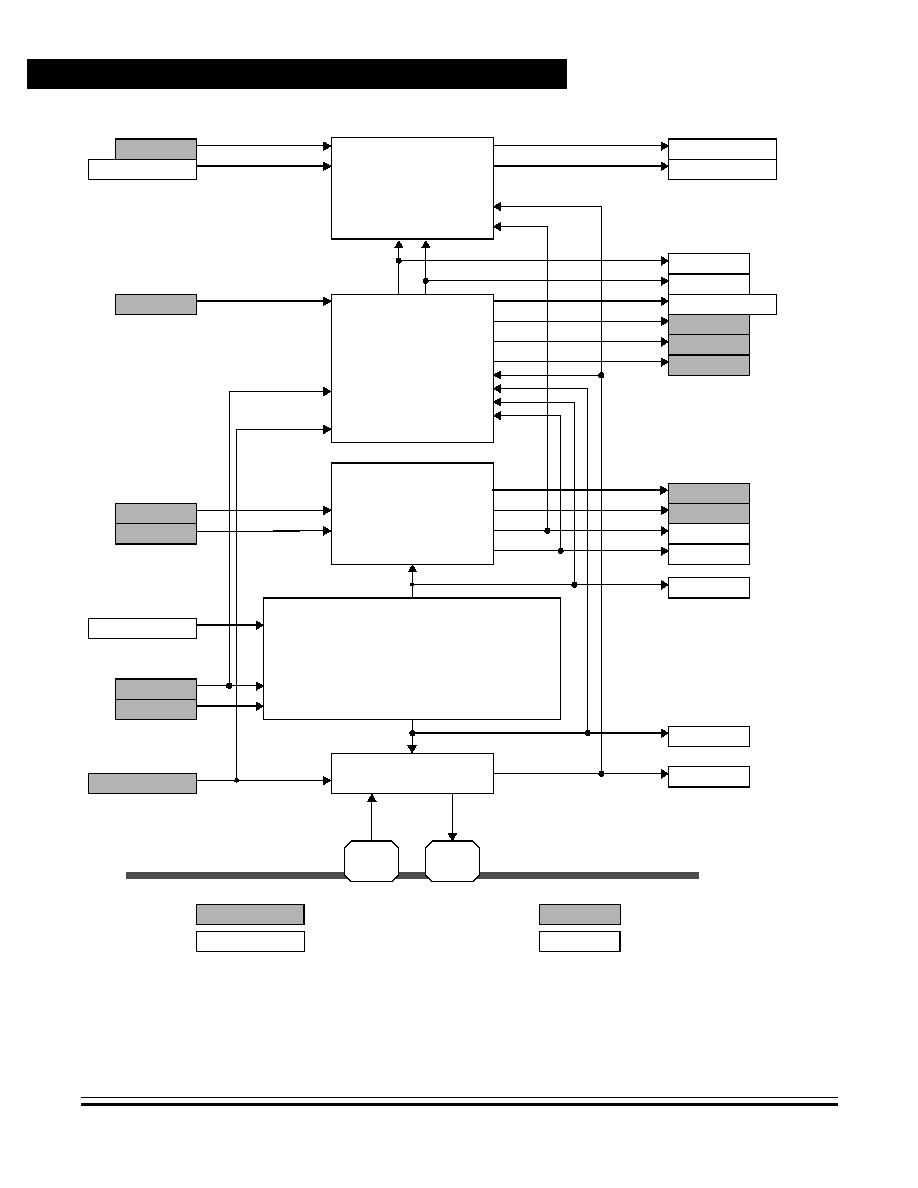
Internal Clock Generator Module (ICG)
Advance Information
MC68HC908RK2
--
Rev. 4.0
110
Internal Clock Generator Module (ICG)
MOTOROLA
Figure 8-1. ICG Module Block Diagram
INTERNAL
TO MCU
EXTERNAL
EXTERNAL CLOCK
GENERATOR
ECGS
OSC1
OSC2
SIMOSCEN
IBASE
ICGS
CMON
CPU_INT
N[6:0]
TRIM[7:0]
CLOCK
MONITOR/SWITCHER
CIRCUIT
CMF
ECLK
ICLK
CLOCK SELECTION
EOFF
IOFF
CGMXCLK
CS
CGMOUT
EXTSLOW
CLOCK ENABLE CIRCUIT
ICGON
ECGON
ECGEN
ICGEN
DSTG
RESET
DDIV
NAME
NAME
NAME
NAME
CONFIGURATION REGISTER BIT
TOP LEVEL SIGNAL
REGISTER BIT
MODULE SIGNAL
CIRCUIT
INTERNAL CLOCK
GENERATOR
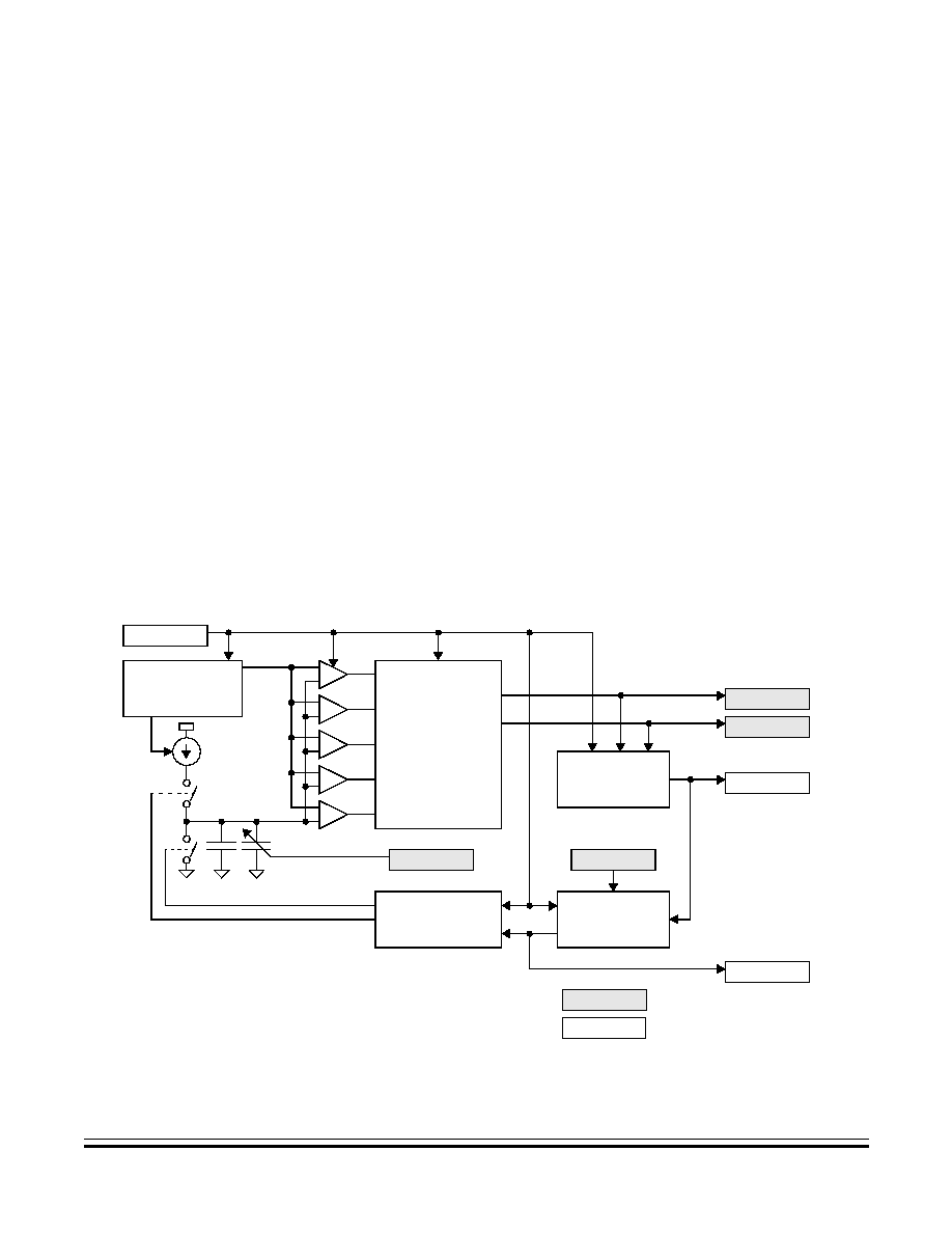
Internal Clock Generator Module (ICG)
Functional Description
MC68HC908RK2
--
Rev. 4.0
Advance Information
MOTOROLA
Internal Clock Generator Module (ICG)
111
8.4.2 Internal Clock Generator
The internal clock generator, shown in
Figure 8-2
, creates a low-
frequency base clock (IBASE), which operates at a nominal frequency
(f
NOM
) of 307.2 kHz
±
25 percent, and an internal clock (ICLK) which is
an integer multiple of IBASE. This multiple is the ICG multiplier factor
(N), which is programmed in the ICG multiplier register (ICGMR). The
internal clock generator is turned off and the output clocks (IBASE and
ICLK) are held low when the internal clock generator enable signal
(ICGEN) is clear.
The internal clock generator contains:
∑
A digitally controlled oscillator
∑
A modulo N divider
∑
A frequency comparator, which contains voltage and current
references, a frequency to voltage converter, and comparators
∑
A digital loop filter
Figure 8-2. Internal Clock Generator Block Diagram
DIGITALLY
CONTROLLED
OSCILLATOR
ICLK
MODULO
N
DIVIDER
FREQUENCY
COMPARATOR
CLOCK GENERATOR
TRIM[7:0]
VOLTAGE &
CURRENT
REFERENCES
DIGITAL
LOOP
FILTER
++
+
≠
≠ ≠
N[6:0]
DSTG[7:0]
ICGEN
IBASE
DDIV[3:0]
NAME
NAME
REGISTER BIT
MODULE SIGNAL

Internal Clock Generator Module (ICG)
Advance Information
MC68HC908RK2
--
Rev. 4.0
112
Internal Clock Generator Module (ICG)
MOTOROLA
8.4.2.1 Digitally Controlled Oscillator
The digitally controlled oscillator (DCO) is an inaccurate oscillator which
generates the internal clock (ICLK). The clock period of ICLK is
dependent on the digital loop filter outputs (DSTG[7:0] and DDIV[3:0]).
Because there is only a limited number of bits in DDIV and DSTG, the
precision of the output (ICLK) is restricted to a long-term precision of
approximately
±
0.202 percent to
±
0.368 percent when measured over
several cycles (of the desired frequency). Additionally, since the
propagation delays of the devices used in the DCO ring oscillator are a
measurable fraction of the bus clock period, reaching the long-term
precision may require alternately running faster and slower than desired,
making the worst case cycle-to-cycle frequency variation
±
6.45 percent
to
±
11.8 percent (of the desired frequency). The valid values of
DDIV:DSTG range from $000 to $9FF. For more information on the
quantization error in the DCO, see
8.5.4 Quantization Error in DCO
Output
.
8.4.2.2 Modulo N Divider
The modulo N divider creates the low-frequency base clock (IBASE) by
dividing the internal clock (ICLK) by the ICG multiplier factor (N)
contained in the ICG multiplier register (ICGMR). When N is
programmed to a $01 or $00, the divider is disabled and ICLK is passed
through to IBASE undivided. When the internal clock generator is stable,
the frequency of IBASE will be equal to the nominal frequency (f
NOM
) of
307.2 kHz
±
25 percent.
8.4.2.3 Frequency Comparator
The frequency comparator effectively compares the low-frequency base
clock (IBASE) to a nominal frequency, f
NOM
. First, the frequency
comparator converts IBASE to a voltage by charging a known capacitor
with a current reference for a period dependent on IBASE. This voltage
is compared to a voltage reference with comparators, whose outputs are
fed to the digital loop filter. The dependence of these outputs on the
capacitor size, current reference, and voltage reference causes up to
±
25 percent error in f
NOM
.
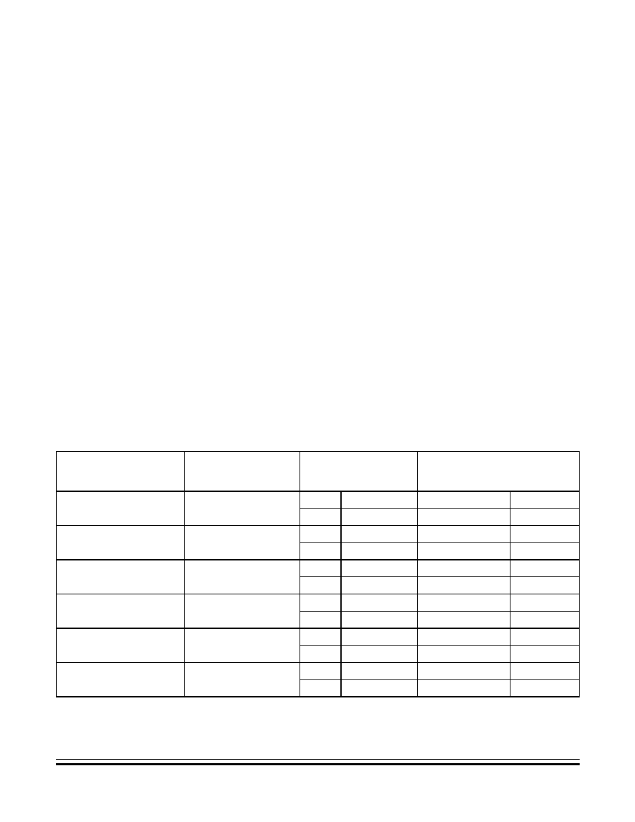
Internal Clock Generator Module (ICG)
Functional Description
MC68HC908RK2
--
Rev. 4.0
Advance Information
MOTOROLA
Internal Clock Generator Module (ICG)
113
8.4.2.4 Digital Loop Filter
The digital loop filter (DLF) uses the outputs of the frequency comparator
to adjust the internal clock (ICLK) clock period. The DLF generates the
DCO divider control bits (DDIV[3:0]) and the DCO stage control bits
(DSTG[7:0]), which are fed to the DCO. The DLF first concatenates the
DDIV and DSTG registers (DDIV[3:0]:DSTG[7:0]) and then adds or
subtracts a value dependent on the relative error in the low-frequency
base clock's period, as shown in
Table 8-1
. In some extreme error
conditions, such as operating at a V
DD
level which is out of specification,
the DLF may attempt to use a value above the maximum ($9FF) or
below the minimum ($000). In both cases, the value for DDIV will be
between $A and $F. In this range, the DDIV value will be interpreted the
same as $9 (the slowest condition). Recovering from this condition
requires subtracting (increasing frequency) in the normal fashion until
the value is again below $9FF (if the desired value is $9xx, the value may
settle at $Axx through $Fxx, an acceptable operating condition). If the
error is less than
±
5 percent, the internal clock generator's filter stable
indicator (FICGS) is set, indicating relative frequency accuracy to the
clock monitor.
Table 8-1. Correction Sizes from DLF to DCO
Frequency Error
of IBASE Compared
to f
NOM
DDVI[3:0]:DSTG[7:0]
Correction
Current to New
DDIV[3:0]:DSTG[7:0]
Relative Correction
in DCO
IBASE < 0.85 f
NOM
≠32 (≠$020)
Min
$xFF to $xDF
≠2/31
≠6.45%
Max
$x20 to $x00
≠2/19
≠10.5%
0.85 f
NOM
< IBASE
IBASE < 0.95 f
NOM
≠8 (≠$008)
Min
$xFF to $xF7
≠0.5/31
≠1.61%
Max
$x08 to $x00
≠0.5/17.5
≠2.86%
0.95 f
NOM
< IBASE
IBASE < f
NOM
≠1 (≠$001)
Min
$xFF to $xFE
≠0.0625/31
≠0.202%
Max
$x01 to $x00
≠0.0625/17.0625
≠0.366%
f
NOM
< IBASE
IBASE < 1.05 f
NOM
+1 (+$001)
Min
$xFE to $xFF
+0.0625/30.9375
+0.202%
Max
$x00 to $x01
+0.0625/17
+0.368%
1.05 f
NOM
< IBASE
IBASE < 1.15 f
NOM
+8 (+$008)
Min
$xF7 to $xFF
+0.5/30.5
+1.64%
Max
$x00 to $x08
+0.5/17
+2.94%
1.15 f
NOM
< IBASE
+32 (+$020)
Min
$xDF to $xFF
+2/29
+6.90%
Max
$x00 to $x20
+2/17
+11.8%
x: Maximum error is independent of value in DDIV[3:0]. DDIV increments or decrements when an addition to DSTG[7:0]
carries or borrows.
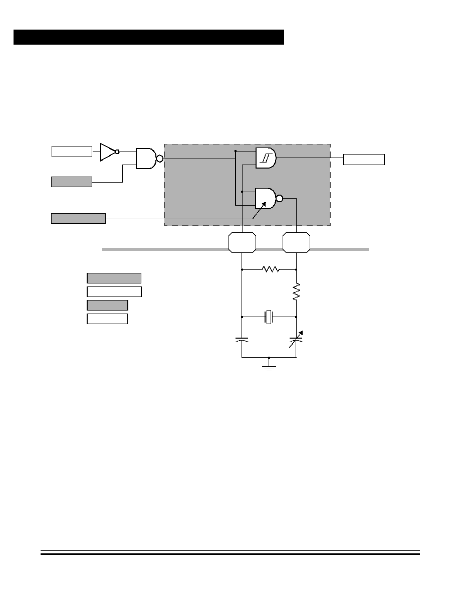
Internal Clock Generator Module (ICG)
Advance Information
MC68HC908RK2
--
Rev. 4.0
114
Internal Clock Generator Module (ICG)
MOTOROLA
8.4.3 External Clock Generator
The ICG also provides for an external oscillator or clock source, if
desired. The external clock generator, shown in
Figure 8-3
, contains an
external oscillator amplifier and an external clock input path.
Figure 8-3. External Clock Generator Block Diagram
8.4.3.1 External Oscillator Amplifier
The external oscillator amplifier provides the gain required by an
external crystal connected in a Pierce oscillator configuration. The
amount of this gain is controlled by the slow external (EXTSLOW) bit in
the configuration register. When EXTSLOW is set, the amplifier gain is
reduced for operating low-frequency crystals (32 kHz to 100 kHz). When
EXTSLOW is clear, the amplifier gain will be sufficient for 1-MHz to
8-MHz crystals. EXTSLOW must be configured correctly for the given
crystal or the circuit may not operate.
C
1
C
2
R
B
X
1
R
S
*
*R
S
can be 0 (shorted) when used
ECLK
INTERNAL TO MCU
EXTERNAL
COMPONENTS REQUIRED FOR
EXTERNAL CRYSTAL USE ONLY
OSC1
OSC2
AMPLIFIER
INPUT PATH
with higher-frequency crystals.
R
efer to manufacturer's data.
EXTSLOW
EXTERNAL
CLOCK
GENERATOR
NAME
NAME
NAME
NAME
CONFIGURATION REGISTER BIT
TOP LEVEL SIGNAL
REGISTER BIT
MODULE SIGNAL
ECGON
STOP

Internal Clock Generator Module (ICG)
Functional Description
MC68HC908RK2
--
Rev. 4.0
Advance Information
MOTOROLA
Internal Clock Generator Module (ICG)
115
The amplifier is enabled when the ECGON bit is set and stop mode is
not enabled. When the amplifier is enabled, it will be connected between
the OSC1 and OSC2 pins. In its typical configuration, the external
oscillator requires five external components:
1. Crystal, X
1
2. Fixed capacitor, C
1
3. Tuning capacitor, C
2
(can also be a fixed capacitor)
4. Feedback resistor, R
B
5. Series resistor, R
S
(included in the diagram to follow strict Pierce
oscillator guidelines and may not be required for all ranges of
operation, especially with high frequency crystals). Refer to the
crystal manufacturer's data for more information.
8.4.3.2 External Clock Input Path
The external clock input path is the means by which the microcontroller
uses an external clock source. The input to the path is the OSC1 pin and
the output is the external clock (ECLK). The path, which contains input
buffering, is enabled when the ECGON bit is set and stop mode is not
enabled.
8.4.4 Clock Monitor Circuit
The ICG contains a clock monitor circuit which, when enabled, will
continuously monitor both the external clock (ECLK) and the internal
clock (ICLK) to determine if either clock source has failed based on these
conditions:
∑
Either ICLK or ECLK has stopped.
∑
The frequency of IBASE < frequency EREF divided by 4
∑
The frequency of ECLK < frequency of IREF divided by 4
Using the clock monitor requires both clocks to be active (ECGON and
ICGON are both set). To enable the clock monitor, both clocks must also
be stable (ECGS and ICGS both set). This is to prevent the use of the
clock monitor when a clock is first turned on and potentially unstable

Internal Clock Generator Module (ICG)
Advance Information
MC68HC908RK2
--
Rev. 4.0
116
Internal Clock Generator Module (ICG)
MOTOROLA
NOTE:
Although the clock monitor can be enabled only when the both clocks are
stable (ICGS or ECGS is set), the clock monitor will remain enabled if
one of the clocks goes unstable.
The clock monitor only works if the external slow (EXTSLOW) bit in the
configuration register is properly defined with respect to the external
frequency source.
The clock monitor circuit, shown in
Figure 8-4
, contains these blocks:
∑
Clock monitor reference generator
∑
Internal clock activity detector
∑
External clock activity detector
8.4.4.1 Clock Monitor Reference Generator
The clock monitor uses a reference based on one clock source to
monitor the other clock source. The clock monitor reference generator
generates the external reference clock (EREF) based on the external
clock (ECLK) and the internal reference clock (IREF) based on the
internal clock (ICLK). To simplify the circuit, the low-frequency base
clock (IBASE) is used in place of ICLK because it always operates at or
near 307.2 kHz. For proper operation, EREF must be at least twice as
slow as IBASE and IREF must be at least twice as slow as ECLK.
To guarantee that IREF is slower than ECLK and EREF is slower than
IBASE, one of the signals is divided down. Which signal is divided and
by how much is determined by the external slow (EXTSLOW) bit in the
configuration register, according to the rules in
Table 8-2
. Note that each
signal (IBASE and ECLK) is always divided by four. A longer divider is
used on either IBASE or ECLK based on the EXTSLOW bit.
NOTE:
If EXTSLOW is not set according to the rules defined in
Table 8-2
, the
clock monitor could switch clock sources unexpectedly.
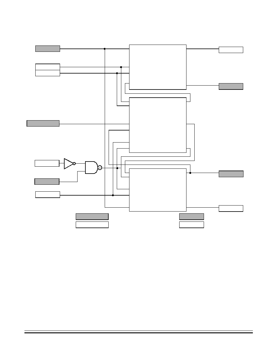
Internal Clock Generator Module (ICG)
Functional Description
MC68HC908RK2
--
Rev. 4.0
Advance Information
MOTOROLA
Internal Clock Generator Module (ICG)
117
Figure 8-4. Clock Monitor Block Diagram
IOFF
CMON
FICGS
IBASE
ICGEN
EREF
IOFF
ICGS
IBASE
EXTXTALEN
EXTSLOW
ECGS
ECGON
ECLK
ICGON
EREF
ESTBCLK
IREF
ESTBCLK
IREF
ECGEN
ECLK
CMON
ECGS
EOFF
ICLK
ACTIVITY
DETECTOR
ECLK
ACTIVITY
DETECTOR
DIVIDER
CMON
EOFF
ECGS
ICGS
IBASE
ICGEN
ECLK
NAME
NAME
NAME
NAME
CONFIGURATION REGISTER BIT
TOP LEVEL SIGNAL
REGISTER BIT
MODULE SIGNAL
ECGON
STOP
EXTSLOW
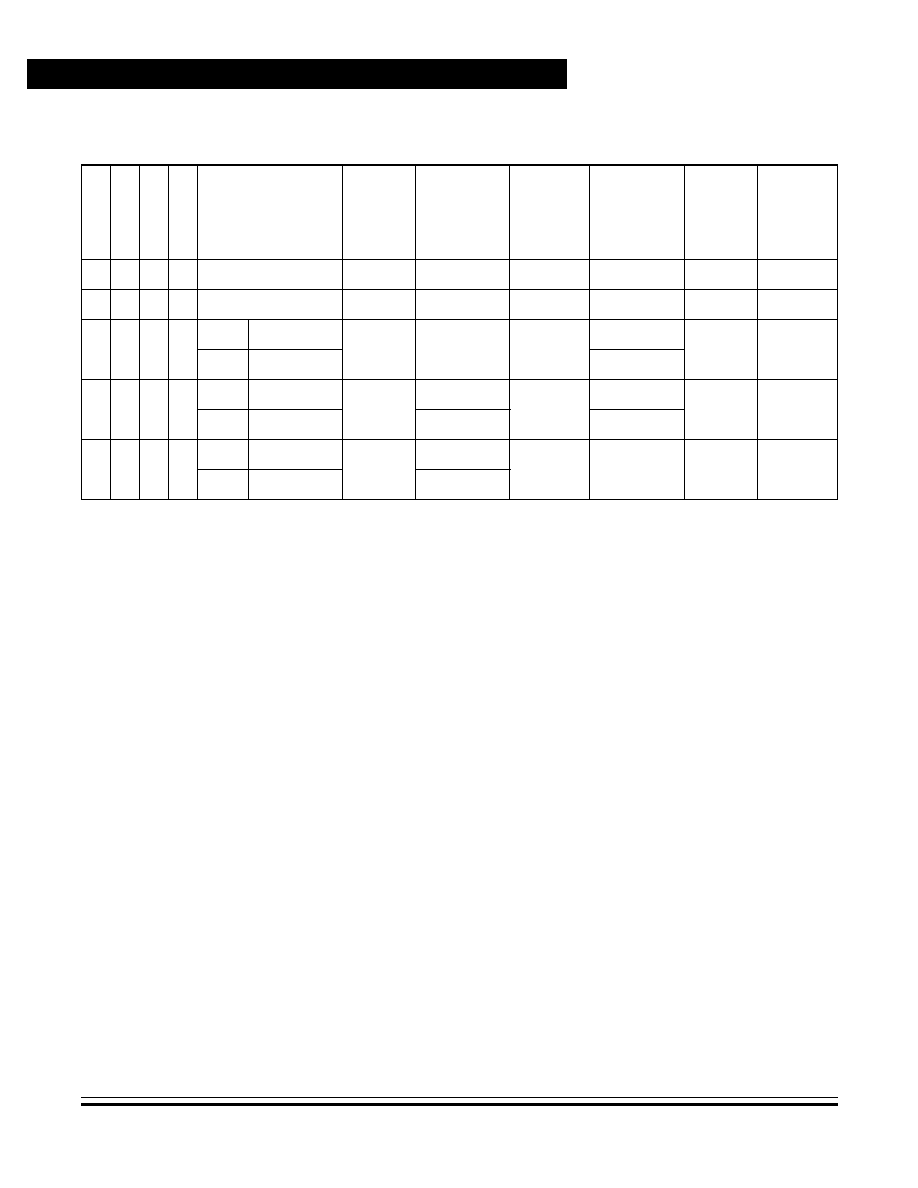
Internal Clock Generator Module (ICG)
Advance Information
MC68HC908RK2
--
Rev. 4.0
118
Internal Clock Generator Module (ICG)
MOTOROLA
The long divider (divide by 4096) is also used as an external crystal
stabilization divider. The divider is reset when the external clock
generator is off (ECGEN is clear). When the external clock generator is
first turned on, the external clock generator stable bit (ECGS) will be
clear. This condition automatically selects ECLK as the input to the long
divider. The external stabilization clock (ESTBCLK) will be ECLK divided
by 4096. This timeout allows the crystal to stabilize. The falling edge of
ESTBCLK is used to set ECGS (ECGS will set after a full 16 or 4096
cycles). When ECGS is set, the divider returns to its normal function.
ESTBCLK may be generated by either IBASE or ECLK, but any clocking
will reinforce only the set condition. If ECGS is cleared because the clock
monitor determined that ECLK was inactive, the divider will revert to a
stabilization divider. Since this will change the EREF and IREF divide
ratios, it is important to turn the clock monitor off (CMON = 0) after
inactivity is detected to ensure valid recovery.
Table 8-2. Clock Monitor Reference Divider Ratios
IC
G
O
N
EC
G
O
N
EC
G
S
EXT
SL
O
W
Ex
t
e
r
n
a
l
Fr
e
q
ue
n
c
y
ER
EF
Di
vi
d
e
r
Ra
t
i
o
ER
EF
Fr
e
q
ue
n
c
y
EST
B
C
L
K
Di
vi
d
e
r
Ra
t
i
o
EST
B
C
L
K
Fr
e
q
ue
n
c
y
IRE
F
Di
vi
d
e
r
Ra
t
i
o
IRE
F
Fr
e
q
ue
n
c
y
0
x
x
x
u
u
u
u
u
off
0
x
0
0
x
0
off
0
off
0
u
u
x
x
0
x
Min
30 kHz
off
0
4096
(ECLK)
1.875 kHz
1*4
76.8 kHz
+/≠ 25%
Max
8 MHz
500 kHz
x
x
1
0
Min
1 MHz
128*4
1.953 kHz
4096
(ECLK)
244 Hz
1*4
76.8 kHz
+/≠ 25%
Max
8 MHz
15.63 kHz
1.953 kHz
x
x
1
1
Min
30 kHz
1*4
7.5 kHz
4096
(IBASE)
75 Hz
+/≠ 25%
16*4
4.8 kHz
+/≠ 25%
Max
100 kHz
25.0 kHz
u: Unaffected; refer to section of table where ICGON or ECGON is set to x (don't care)
[IBASE is always used as the internal frequency (307.2 kHz).]

Internal Clock Generator Module (ICG)
Functional Description
MC68HC908RK2
--
Rev. 4.0
Advance Information
MOTOROLA
Internal Clock Generator Module (ICG)
119
8.4.4.2 Internal Clock Activity Detector
The internal clock activity detector looks for at least one falling edge on
the low-frequency base clock (IBASE) every time the external reference
(EREF) is low. Since EREF is less than half the frequency of IBASE, this
should occur every time. If it does not occur two consecutive times, the
internal clock inactivity indicator (IOFF) is set. IOFF will be cleared the
next time there is a falling edge of IBASE while EREF is low.
The internal clock stable bit (ICGS) is set when IBASE is within
approximately 5 percent of the target 307.2 kHz
±
25 percent for two
consecutive measurements. ICGS is cleared when IBASE is outside the
5 percent of the target 307.2 kHz
±
25 percent, the internal clock
generator is disabled (ICGEN is clear), or when IOFF is set.
8.4.4.3 External Clock Activity Detector
The external clock activity detector looks for at least one falling edge on
the external clock (ECLK) every time the internal reference (IREF) is low.
Since IREF is less than half the frequency of ECLK, this should occur
every time. If it does not occur two consecutive times, the external clock
inactivity indicator (EOFF) is set. EOFF will be cleared the next time
there is a falling edge of ECLK while IREF is low.
The external clock stable bit (ECGS) is also generated in the external
clock activity detector. ECGS is set on a falling edge of the external
stabilization clock (ESTBCLK). This will be 4096 ECLK cycles after the
external clock generator on bit (ECGON) is set. ECGS is cleared when
the external clock generator is disabled (ECGON is clear) or when EOFF
is set.
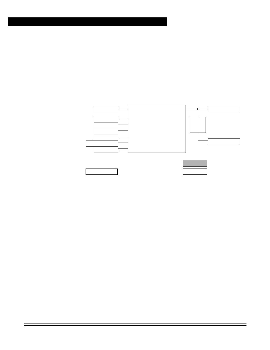
Internal Clock Generator Module (ICG)
Advance Information
MC68HC908RK2
--
Rev. 4.0
120
Internal Clock Generator Module (ICG)
MOTOROLA
8.4.5 Clock Selection Circuit
The clock selection circuit, shown in
Figure 8-5
, contains two clock
switches which generate the oscillator output clock (CGMXCLK) from
either the internal clock (ICLK) or the external clock (ECLK). The clock
selection circuit also contains a divide-by-two circuit which creates the
clock generator output clock (CGMOUT), which generates the bus
clocks.
Figure 8-5. Clock Selection Circuit Block Diagram
8.4.5.1 Clock Selection Switch
The clock select switch creates the oscillator output clock (CGMXCLK)
from either the internal clock (ICLK) or the external clock (ECLK), based
on the clock select bit (CS; set selects ECLK, clear selects ICLK). When
switching the CS bit, both ICLK and ECLK must be on (ICGON and
ECGON set). The clock being switched to must also be stable (ICGS or
ECGS set).
ICLK
ECLK
IOFF
EOFF
FORCE_I
FORCE_E
SELECT
OUTPUT
SYNCHRONIZING
CLOCK
SWITCHER
DIV2
NAME
NAME
NAME
TOP LEVEL SIGNAL
REGISTER BIT
MODULE SIGNAL
RESET
ECLK
EOFF
ICLK
IOFF
V
SS
CS
CGMOUT
CGMXCLK
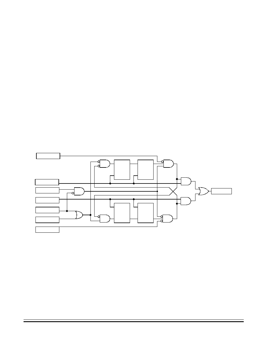
Internal Clock Generator Module (ICG)
Functional Description
MC68HC908RK2
--
Rev. 4.0
Advance Information
MOTOROLA
Internal Clock Generator Module (ICG)
121
8.4.5.2 Clock Switching Circuit
To robustly switch between the internal clock (ICLK) and the external
clock (ECLK), the switch assumes the clocks are completely
asynchronous, so a synchronizing circuit is required to make the
transition (see
Figure 8-6
). When the clock select bit is changed, the
switch will continue to operate off the original clock for between 1 and 2
cycles as the select input transitions through one side of the
synchronizer. Next, the output will be held low for between 1 and 2
cycles of the new clock as the select input transitions through the other
side. Then the output starts switching at the new clock's frequency. This
transition guarantees that no glitches will be seen on the output even
though the select input may change asynchronously to the clocks. The
unpredictably of the transition period is a necessary result of the
asynchronicity.
Figure 8-6. Synchronizing Clock Switcher Circuit Diagram
FORCE_I
ECLK
EOFF
OUTPUT
D
Q
CK
DFF
QB
SELECT
ICLK
D
Q
CK
DFF
QB
D
Q
CK
DFF
QB
D
Q
CK
DFF
QB
FORCE_E
FORCE_I = Force internal; reset condition
FORCE_E = Force external
IOFF

Internal Clock Generator Module (ICG)
Advance Information
MC68HC908RK2
--
Rev. 4.0
122
Internal Clock Generator Module (ICG)
MOTOROLA
The switch automatically selects ICLK during reset. When the clock
monitor is on (CMON is set) and it determines one of the clock sources
is inactive (as indicated by the IOFF or EOFF signals), the circuit is
forced to select the active clock. There are no clocks for the inactive side
of the synchronizer to properly operate, so that side is forced deselected.
However, the active side will not be selected until one to two clock cycles
after the IOFF or EOFF signal transitions.
8.5 Usage Notes
The ICG has several features which can provide protection to the
microcontroller if properly used. There are other features which can
greatly simplify usage of the ICG if certain techniques are employed.
This section will describe several possible ways to use the ICG and its
features. These techniques are not the only ways to use the ICG, and
may not be optimum for all environments. In any case, these techniques
should be used only as a template, and the user should modify them
according to the application's requirements.
These notes include:
∑
Switching clock sources
∑
Enabling the clock monitor
∑
Using clock monitor interrupts
∑
Quantization error in DCO output
∑
Switching internal clock frequencies
∑
Nominal frequency settling time
∑
Improving frequency settling time
∑
Trimming frequency

Internal Clock Generator Module (ICG)
Usage Notes
MC68HC908RK2
--
Rev. 4.0
Advance Information
MOTOROLA
Internal Clock Generator Module (ICG)
123
8.5.1 Switching Clock Sources
Switching from one clock source to another requires both clock sources
to be enabled and stable. A simple flow requires:
1. Enable desired clock source
2. Wait for it to become stable
3. Switch clocks
4. Disable previous clock source
The key point to remember in this flow is that the clock source cannot be
switched (CS cannot be written) unless the desired clock is on and
stable.
A short assembly code example of how to employ this flow is shown in
Figure 8-7
. This code is for illustrative purposes only and does not
represent valid syntax for any particular assembler.
Figure 8-7. Code Example for Switching Clock Sources
;Clock Switching Code Example
;This code switches from Internal to External clock
;Clock Monitor and interrupts are not enabled
start
lda
#$13
;Mask for CS, ECGON, ECGS
;If switching from External to Internal, mask is $0C.
loop
**
**
;Other code here, such as writing the COP, since ECGS may
;take some time to set
sta
icgcr
;Try to set CS, ECGON and clear ICGON. ICGON will not
;clear until CS is set, and CS will not set until
;ECGON and ECGS are set.
cmpa
icgcr
;Check to see if ECGS set, then CS set, then ICGON clear
bne
loop
;Keep looping until ICGON is clear.

Internal Clock Generator Module (ICG)
Advance Information
MC68HC908RK2
--
Rev. 4.0
124
Internal Clock Generator Module (ICG)
MOTOROLA
8.5.2 Enabling the Clock Monitor
Many applications require the clock monitor to determine if one of the
clock sources has become inactive, so the other can be used to recover
from a potentially dangerous situation. Using the clock monitor requires
both clocks to be active (ECGON and ICGON both set). To enable the
clock monitor, both clocks also must be stable (ECGS and ICGS both
set). This is to prevent the use of the clock monitor when a clock is first
turned on and potentially unstable.
Enabling the clock monitor and clock monitor interrupts requires a flow
similar to this flow:
1. Enable the alternate clock source
2. Wait for both clock sources to be stable
3. Switch to the desired clock source if necessary
4. Enable the clock monitor
5. Enable clock monitor interrupts
These events must happen in sequence. A short assembly code
example of how to employ this flow is shown in
Figure 8-8
. This code is
for illustrative purposes only and does not represent valid syntax for any
particular assembler.
Figure 8-8. Code Example for Enabling the Clock Monitor
;Clock Monitor Enabling Code Example
;This code turns on both clocks, selects the desired
; one, then turns on the Clock Monitor and Interrupts
start
lda
#$AF
;Mask for CMIE, CMON, ICGON, ICGS, ECGON, ECGS
; If Internal Clock desired, mask is $AF
; If External Clock desired, mask is $BF
; If interrupts not desired mask is $2F int; $3F ext
loop
**
**
;Other code here, such as writing the COP, since ECGS
; and ICGS may take some time to set.
sta
icgcr
;Try to set CMIE. CMIE wont set until CMON set; CMON
; won't set until ICGON, ICGS, ECGON, ECGS set.
brset
6,ICGCR,error
;Verify CMF is not set
cmpa
icgcr
;Check if ECGS set, then CMON set, then CMIE set
bne
loop
;Keep looping until CMIE is set.

Internal Clock Generator Module (ICG)
Usage Notes
MC68HC908RK2
--
Rev. 4.0
Advance Information
MOTOROLA
Internal Clock Generator Module (ICG)
125
8.5.3 Clock Monitor Interrupts
The clock monitor circuit can be used to recover from perilous situations
such as crystal loss. To use the clock monitor effectively, these notes
should be observed:
∑
Enable the clock monitor and clock monitor interrupts.
∑
The first statement in the clock monitor interrupt service routine
should be a read to the ICG control register (ICGCR) to verify that
the clock monitor flag (CMF) is set. This is also the first step in
clearing the CMF bit.
∑
Never use BSET or BCLR instructions on the ICGCR, as this may
inadvertently clear CMF. Only use the BRSET and BRCLR
instructions to check the CMF bit and not to check any other bits
in the ICGCR.
∑
When the clock monitor detects inactivity on the selected clock
source (defined by the CS bit of the ICG control register), the
inactive clock is deselected automatically and the remaining active
clock is selected as the source for CGMXCLK. The interrupt
service routine can use the state of the CS bit to check which clock
is inactive.
∑
When the clock monitor detects inactivity, the application may
have been subjected to extreme conditions which may have
affected other circuits. The clock monitor interrupt service routine
should take any appropriate precautions.
8.5.4 Quantization Error in DCO Output
The digitally controlled oscillator (DCO) is comprised of three major sub-
blocks:
1. Binary weighted divider
2. Variable-delay ring oscillator
3. Ring oscillator fine-adjust circuit
Each of these blocks affects the clock period of the internal clock (ICLK).
Since these blocks are controlled by the digital loop filter (DLF) outputs

Internal Clock Generator Module (ICG)
Advance Information
MC68HC908RK2
--
Rev. 4.0
126
Internal Clock Generator Module (ICG)
MOTOROLA
DDIV and DSTG, the output of the DCO can change only in quantized
steps as the DLF increments or decrements its output. The following
sections describe how each block will affect the output frequency.
8.5.4.1 Digitally Controlled Oscillator
The digitally controlled oscillator (DCO) is an inaccurate oscillator which
generates the internal clock (ICLK), whose clock period is dependent on
the digital loop filter outputs (DSTG[7:0] and DDIV[3:0]). Because of the
digital nature of the DCO, the clock period of ICLK will change in
quantized steps. This will create a clock period difference or quantization
error (Q-ERR) from one cycle to the next. Over several cycles or for
longer periods, this error is divided out until it reaches a minimum error
of 0.202 percent to 0.368 percent. The dependence of this error on the
DDIV[3:0] value and the number of cycles the error is measured over is
shown in
Table 8-3
.
8.5.4.2 Binary Weighted Divider
The binary weighted divider divides the output of the ring oscillator by a
power of 2, specified by the DCO divider control bits (DDIV[3:0]). DDIV
maximizes at %1001 (values of %1010 through %1111 are interpreted
as %1001), which corresponds to a divide by 512. When DDIV is %0000,
Table 8-3. Quantization Error in ICLK
DDIV[3:0]
ICLK Cycles
Bus Cycles
ICLK
Q-ERR
%0000 (min)
4
1
1.61%≠2.94%
%0000 (min)
32
8
0.202%≠0.368%
%0001
4
1
0.806%≠1.47%
%0001
16
4
0.202%≠0.368%
%0010
4
1
0.403%≠0.735%
%0010
8
2
0.202%≠0.368%
%0011
4
1
0.202%≠0.368%
%0100
2
1
0.202%≠0.368%
%0101≠%1001 (max)
1
1
0.202%≠0.368%

Internal Clock Generator Module (ICG)
Usage Notes
MC68HC908RK2
--
Rev. 4.0
Advance Information
MOTOROLA
Internal Clock Generator Module (ICG)
127
the ring oscillator's output is divided by 1. Incrementing DDIV by one will
double the period; decrementing DDIV will halve the period. The DLF
cannot directly increment or decrement DDIV; DDIV is only incremented
or decremented when an addition or subtraction to DSTG carries or
borrows.
8.5.4.3 Variable-Delay Ring Oscillator
The variable-delay ring oscillator's period is adjustable from 17 to 31
stage delays, in increments of two, based on the upper three DCO stage
control bits (DSTG[7:5]). A DSTG[7:5] of %000 corresponds to 17 stage
delays; DSTG[7:5] of %111 corresponds to 31 stage delays. Adjusting
the DSTG[5] bit has a 6.45 percent to 11.8 percent effect on the output
frequency. This also corresponds to the size correction made when the
frequency error is greater than
±
15 percent. The value of the binary
weighted divider does not affect the relative change in output clock
period for a given change in DSTG[7:5].
8.5.4.4 Ring Oscillator Fine-Adjust Circuit
The ring oscillator fine-adjust circuit causes the ring oscillator to
effectively operate at non-integer numbers of stage delays by operating
at two different points for a variable number of cycles specified by the
lower five DCO stage control bits (DSTG[4:0]). For example, when
DSTG[7:5] is %011, the ring oscillator nominally operates at 23 stage
delays. When DSTG[4:0] is %00000, the ring will always operate at 23
stage delays. When DSTG[4:0] is %00001, the ring will operate at 25
stage delays for one of 32 cycles and at 23 stage delays for 31 of 32
cycles. Likewise, when DSTG[4:0] is %11111, the ring operates at 25
stage delays for 31 of 32 cycles and at 23 stage delays for one of 32
cycles. When DSTG[7:5] is %111, similar results are achieved by
including a variable divide-by-two, so the ring operates at 31 stages for
some cycles and at 17 stage delays, with a divide-by-two for an effective
34 stage delays, for the remainder of the cycles. Adjusting the DSTG[0]
bit has a 0.202 percent to 0.368 percent effect on the output clock period.
This corresponds to the minimum size correction made by the DLF, and
the inherent, long-term quantization error in the output frequency.

Internal Clock Generator Module (ICG)
Advance Information
MC68HC908RK2
--
Rev. 4.0
128
Internal Clock Generator Module (ICG)
MOTOROLA
8.5.5 Switching Internal Clock Frequencies
The frequency of the internal clock (ICLK) may need to be changed for
some applications. For example, if the reset condition does not provide
the correct frequency, or if the clock is slowed down for a low-power
mode (or sped up after a low-power mode), the frequency must be
changed by programming the internal clock multiplier factor (N). The
frequency of ICLK is N times the frequency of IBASE, which is 307.2 kHz
±
25 percent.
Before switching frequencies by changing the N value, the clock monitor
must be disabled. This is because when N is changed, the frequency of
the low-frequency base clock (IBASE) will change proportionally until the
digital loop filter has corrected the error. Since the clock monitor uses
IBASE, it could erroneously detect an inactive clock. The clock monitor
cannot be re-enabled until the internal clock is stable again (ICGS is set).
NOTE:
There is no hardware mechanism to prevent changing bus frequency
dynamically. Be careful when changing bus frequency and consider the
impact on the system.
This flow is an example of how to change the clock frequency:
1. Verify there is no clock monitor interrupt by reading the CMF bit.
2. Turn off the clock monitor.
3. If desired, switch to the external clock (see
8.5.1 Switching Clock
Sources
).
4. Change the value of N.
5. Switch back to internal (see
8.5.1 Switching Clock Sources
),
if desired.
6. Turn on the clock monitor (see
8.5.2 Enabling the Clock
Monitor
), if desired.

Internal Clock Generator Module (ICG)
Usage Notes
MC68HC908RK2
--
Rev. 4.0
Advance Information
MOTOROLA
Internal Clock Generator Module (ICG)
129
8.5.6 Nominal Frequency Settling Time
Because the clock period of the internal clock (ICLK) is dependent on the
digital loop filter outputs (DDIV and DSTG) which cannot change
instantaneously, ICLK will temporarily operate at an incorrect clock
period when any of the operating condition changes. This happens
whenever the part is reset, the ICG multiply factor (N) is changed, the
ICG trim factor (TRIM) is changed, or the internal clock is enabled after
inactivity (STOP or disabled operation). The time that the ICLK takes to
adjust to the correct period is known as the settling time.
Settling time depends primarily on how many corrections it takes to
change the clock period, and the period of each correction. Since the
corrections require four periods of the low-frequency base clock
(4*t
IBASE
), and since ICLK is N (the ICG multiply factor for the desired
frequency) times faster than IBASE, each correction takes 4*N*t
ICLK
.
The period of ICLK, however, will vary as the corrections occur.
8.5.6.1 Settling to Within 15 Percent
When the error is greater than 15 percent, the filter takes eight
corrections to double or halve the clock period. Due to how the DCO
increases or decreases the clock period, the total period of these eight
corrections is approximately 11 times the period of the fastest correction.
(If the corrections were perfectly linear, the total period would be 11.5
times the minimum period; however, the ring must be slightly non-linear.)
Therefore, the total time it takes to double or halve the clock period is
44*N*t
ICLKFAST
.
If the clock period needs more than doubled or halved, the same
relationship applies, only for each time the clock period needs doubled,
the total number of cycles doubles.
That is, when transitioning from fast to slow:
∑
Going from the initial speed to half speed takes 44*N*t
ICLKFAST
∑
From half speed to quarter speed takes 88*N*t
ICLKFAST
∑
Going from quarter speed to eighth speed takes 176*N*t
ICLKFAST
,
and so on.

Internal Clock Generator Module (ICG)
Advance Information
MC68HC908RK2
--
Rev. 4.0
130
Internal Clock Generator Module (ICG)
MOTOROLA
This series can be expressed as (2
x
≠1)*44*N*t
ICLKFAST
, where x is the
number of times the speed needs doubled or halved. Since 2
x
happens
to be equal to t
ICLKSLOW
/t
ICLKFAST
, the equation reduces to
44*N*(t
ICLKSLOW
-t
ICLKFAST
). Note that increasing speed takes much
longer than decreasing speed since N is higher. This can be expressed
in terms of the initial clock period (t
1
) minus the final clock period (t
2
) as
such:
8.5.6.2 Settling to Within 5 Percent
Once the clock period is within 15 percent of the desired clock period,
the filter starts making smaller adjustments. When between 15 percent
and 5 percent error, each correction will adjust the clock period between
1.61 percent and 2.94 percent. In this mode, a maximum of eight
corrections will be required to get to less than 5 percent error. Since the
clock period is relatively close to desired, each correction takes
approximately the same period of time, or 4*t
IBASE
. At this point, the
internal clock stable bit (ICGS) will be set and the clock frequency is
usable, although the error will be as high as 5 percent. The total time to
this point is:
8.5.6.3 Total Settling Time
Once the clock period is within 5 percent of the desired clock period, the
filter starts making minimum adjustments. In this mode, each correction
will adjust the frequency between 0.202 percent and 0.368 percent. A
maximum of 24 corrections will be required to get to the minimum error.
Each correction takes approximately the same period of time or 4*t
IBASE
.
Added to the corrections for 15 percent to 5 percent, this makes 32
corrections (128*t
IBASE
) to get from 15 percent to the minimum error.
The total time to the minimum error is:
t
15
abs 44
N t
1
t
2
≠
(
)
[
]
=
t
5
abs 44
N t
1
t
2
≠
(
)
[
]
32
t
IBASE
+
=
t
tot
abs 44
N t
1
t
2
≠
(
)
[
]
128
t
IBASE
+
=

Internal Clock Generator Module (ICG)
Usage Notes
MC68HC908RK2
--
Rev. 4.0
Advance Information
MOTOROLA
Internal Clock Generator Module (ICG)
131
The equations for t
15
, t
5
, and t
tot
are dependent on the actual initial and
final clock periods t
1
and t
2
, not the nominal. This means the variability
in the ICLK frequency due to process, temperature, and voltage must be
considered. Additionally, other process factors and noise can affect the
actual tolerances of the points at which the filter changes modes. This
means a worst case adjustment of up to 35 percent (ICLK clock period
tolerance plus 10 percent) must be added. This adjustment can be
reduced with trimming.
Table 8-4
shows some typical values for settling
time.
8.5.7 Improving Settling Time
The settling time of the internal clock generator can be vastly improved
if an external clock source can be used during the settling time. When
the internal clock generator is disabled (ICGON is low), the DDIV[3:0]
and DSTG[7:0] bits can be written. Then, when the internal clock
generator is re-enabled, the clock period will automatically start at the
point written in the DDIV and DSTG bits.
Since a change in the DDIV and DSTG bits only cause a change in the
clock period relative to the starting point, the starting point must first be
captured. The initial clock period can be expressed as in the next
example, where t
X
is a process, temperature, and voltage dependent
constant and DDIV1 and DSTG1 are the values of DDIV and DSTG
when operating at t
1
.
Table 8-4. Typical Settling Time Examples
t
1
t
2
N
t
15
t
5
t
tot
1/ (6.45 MHz)
1/ (25.8 MHz)
84
430
µ
s
535
µ
s
850
µ
s
1/ (25.8 MHz)
1/ (6.45 MHz)
21
107
µ
s
212
µ
s
525
µ
s
1/ (25.8 MHz)
1/ (307.2 kHz)
1
141
µ
s
246
µ
s
560
µ
s
1/ (307.2 kHz)
1/ (25.8 MHz)
84
11.9 ms
12.0 ms
12.3 ms
t
1
t
X
2
DDIV1
DSTG1
=

Internal Clock Generator Module (ICG)
Advance Information
MC68HC908RK2
--
Rev. 4.0
132
Internal Clock Generator Module (ICG)
MOTOROLA
Finding the new values for DDIV and DSTG is easy if the new clock
period is a binary multiple or fraction of the original. In this case, DSTG
is unchanged and DDIV2 is DDIV1 + log
2
(t
2
/t
1
).
If the new clock period is not a binary multiple or fraction of the original,
both DSTG and DDIV may need to change according to these
equations:
If DSTG2 is greater than 255:
The software required to do this is relatively simple, since most of the
math can be done before coding because the initial and final clock
periods are known. An example of how to code this in assembly code is
shown in
Figure 8-9
. This example is for illustrative purposes only and
does not represent a valid syntax for any particular assembler.
DVFACT
int
t
2
t
1
/
(
)
log
2
( )
log
----------------------------
=
DDIV2
DDIV1
DVFACT
+
=
DSFACT
t
2
t
1
/
(
)
2
DDIV2
DDIV1
≠
(
)
---------------------------------------
=
DSTG2
DSFACT DSTG1
=
DDIV2
DDIV2
1
+
=
DSTG2
DSTG2
2
------------------
=

Internal Clock Generator Module (ICG)
Usage Notes
MC68HC908RK2
--
Rev. 4.0
Advance Information
MOTOROLA
Internal Clock Generator Module (ICG)
133
Figure 8-9. Code Example for Writing DDIV and DSTG
8.5.8 Trimming Frequency on the Internal Clock Generator
The unadjusted frequency of the low-frequency base clock (IBASE),
when the comparators in the frequency comparator indicate zero error,
will vary as much as
±
25 percent due to process, temperature, and
voltage dependencies. These dependencies are in the voltage and
current references, the offset of the comparators, and the internal
capacitor. The voltage and temperature dependencies have been
designed to be a maximum of approximately
±
1 percent error. The
process dependencies account for the rest.
;DDIV and DSTG modification code example
;Changes DDIV and DSTG according to the initial and
; desired clock period values
;Requires ICGON to be clear (disabled)
;User must previously calculate DVFACT and STFACT by
; the equations listed in the specification
;Modifies X and A registers
start
lda
icgcr
;Verify ICGON clear (this will require
cmp
#13
; CMIE,CMF,CMON,ICGON,ICGS clear and CS,ECGON,ECGS set)
lda
#dvfact
;Add the DDIV factor (calculated before
add
icgdvr
; coding by the DDIV2 equation)
sta
icgdvr
lda
#stfact
;Load the DSTG factor (calculated before coding and
; multiplied by 128 to make it 0-255 for maximum precision
ldx
icgdsr
;Load current stage register contents
mul
;Multiply factor times current value
rola
;Since factor was multiplied by 128,
rolx
; result is x6-x0:a7, so put it all in X
bcc
store
;If result is >255, rolx will set carry
rorx
; so divide result by two and
inc
; add one to DDIV
store
stx
icgdsr
;Store value
lda
icgdvr
;Test to see if DDIV too high or low
cmp
#09
;Valid range 0-9; too low is FF/FE; too high is 0A/0B
bhi
exit
;If DDIV is 0-9, you're almost done
lda
#09
;Otherwise, maximize period and execute error code
sta
icgdvr
jmp
error
exit
jmp
enable
;Jump to code which turns on desired
;clock, clock monitor, interrupts, etc.

Internal Clock Generator Module (ICG)
Advance Information
MC68HC908RK2
--
Rev. 4.0
134
Internal Clock Generator Module (ICG)
MOTOROLA
Fortunately, for an individual part, the process dependencies are
constant. An individual part can operate at approximately
±
2 percent
variance from its unadjusted operating point over the entire specification
range of the application. If the unadjusted operating point can be
changed, the entire variance can be limited to
±
2 percent.
The method of changing the unadjusted operating point is by changing
the size of the capacitor. This capacitor is designed with 639 equally
sized units. 384 of which are always connected. The remaining 255 units
are put in by adjusting the ICG trim factor (TRIM). The default value for
TRIM is $80, or 128 units, making the default capacitor size 512. Each
unit added or removed will adjust the output frequency by about
±
0.195
percent of the unadjusted frequency (adding to TRIM will decrease
frequency). Therefore, the frequency of IBASE can be changed to
±
25
percent of its unadjusted value, which is enough to cancel the process
variability mentioned before.
The best way to trim the internal clock is to use the timer to measure the
width of an input pulse on an input capture pin (this pulse must be
supplied by the application and should be as long or wide as possible).
Considering the prescale value of the timer and the theoretical (zero
error) frequency of the bus (307.2 kHz *N/4), the error can be calculated.
This error, expressed as a percentage, can be divided by 0.195 percent
and the resultant factor added or subtracted from TRIM. This process
should be repeated to eliminate any residual error.
NOTE:
It is recommended that the user preserve a copy of the contents of the
ICG trim register (ICGTR) in non-volitale memory.
Address $7FEF is reserved for an optional factory-determined value.
Consult with a local Motorola representative for more information and
availability of this option.

Internal Clock Generator Module (ICG)
Low-Power Modes
MC68HC908RK2
--
Rev. 4.0
Advance Information
MOTOROLA
Internal Clock Generator Module (ICG)
135
8.6 Low-Power Modes
The WAIT and STOP instructions put the MCU in low power-
consumption standby modes.
8.6.1 Wait Mode
The ICG remains active in wait mode. If enabled, the ICG interrupt to the
CPU can bring the MCU out of wait mode.
In some applications, low-power consumption is desired in wait mode
and a high-frequency clock is not needed. In these applications, reduce
power consumption by either selecting a low-frequency external clock
and turn the internal clock generator off, or reduce the bus frequency by
minimizing the ICG multiplier factor (N) before executing the WAIT
instruction.
8.6.2 Stop Mode
The ICG is disabled in stop mode. Upon execution of the STOP
instruction, all ICG activity will cease and the output clocks (CGMXCLK
and CGMOUT) will be held low. Power consumption will be minimal.
The STOP instruction does not affect the values in the ICG registers.
Normal execution will resume after the MCU exits stop mode.
8.7 Configuration Register Option
One configuration register option affects the functionality of the ICG:
EXTSLOW (slow external clock).
All configuration register options will have a default setting. Refer to
Section 9. Configuration Register (CONFIG)
on how the configuration
register is used.

Internal Clock Generator Module (ICG)
Advance Information
MC68HC908RK2
--
Rev. 4.0
136
Internal Clock Generator Module (ICG)
MOTOROLA
8.7.1 EXTSLOW
Slow external clock (EXTSLOW), when set, will decrease the drive
strength of the oscillator amplifier, enabling low-frequency crystal
operation (30 kHz≠100 kHz). When clear, EXTSLOW enables high
frequency crystal operation (1 MHz to 8 MHz).
EXTSLOW, when set, also configures the clock monitor to expect an
external clock source that is slower than the low-frequency base clock
(60 Hz≠307.2 kHz). When EXTSLOW is clear, the clock monitor will
expect an external clock faster than the low-frequency base clock
(307.2 kHz≠32 MHz).
The default state for this option is clear.
8.8 I/O Registers
The ICG contains five registers, summarized in
Figure 8-10
. These
registers are:
∑
ICG control register, ICGCR
∑
ICG multiplier register, ICGMR
∑
ICG trim register, ICGTR
∑
ICG DCO divider control register, ICGDVR
∑
ICG DCO stage control register, ICGDSR
Several of the bits in these registers have interaction where the state of
one bit may force another bit to a particular state or prevent another bit
from being set or cleared. A summary of this interaction is shown in
Table 8-5
.
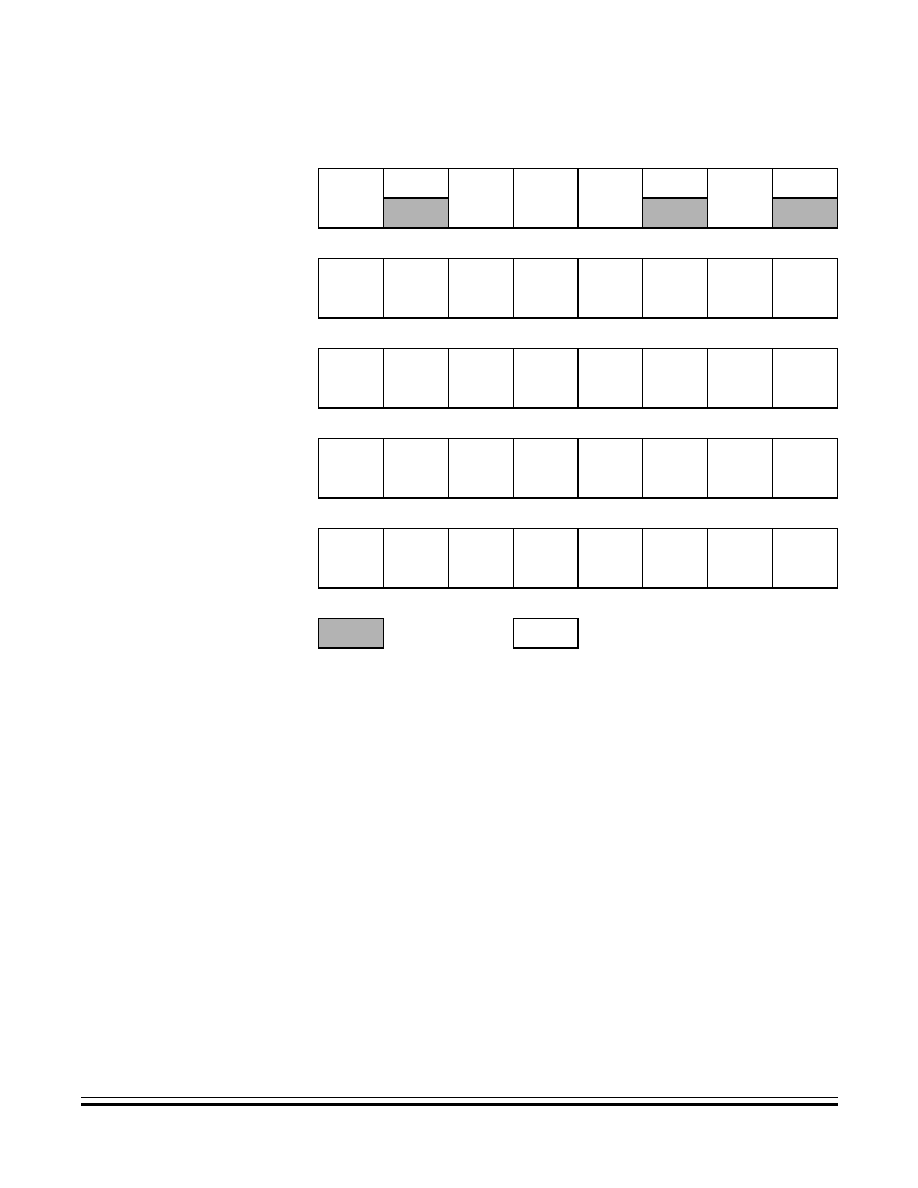
Internal Clock Generator Module (ICG)
I/O Registers
MC68HC908RK2
--
Rev. 4.0
Advance Information
MOTOROLA
Internal Clock Generator Module (ICG)
137
Addr.
Register Name
Bit 7
6
5
4
3
2
1
Bit 0
$0036
Internal Clock Generator
Control Register
(ICGCR)
See page 139.
Read:
CMIE
CMF
CMON
CS
ICGON
ICGS
ECGON
ECGS
Write:
Reset:
0
0
0
0
1
0
0
0
$0037
Internal Clock Generator
Multiplier Register
(ICGMR)
See page 141.
Read:
R
N6
N5
N4
N3
N2
N1
N0
Write:
Reset:
0
0
0
1
0
1
0
1
$0038
Internal Clock Generator
Trim Register (ICGTR)
See page 142.
Read:
TRIM7
TRIM6
TRIM5
TRIM4
TRIM3
TRIM2
TRIM1
TRIM0
Write:
Reset:
1
0
0
0
0
0
0
0
$0039
I
CG DCO Divider Control
Register (ICGDVR)
See page 143.
Read:
R
R
R
R
DDIV3
DDIV2
DDIV1
DDIV0
Write:
Reset:
0
0
0
0
U
U
U
U
$003A
ICG DCO Stage Register
(ICGDSR)
See page 144.
Read:
DSTG7
DSTG6
DSTG5
DSTG4
DSTG3
DSTG2
DSTG1
DSTG0
Write:
Reset:
Unaffected by reset
= Unimplemented
R
= Reserved
U = Unaffected
Figure 8-10. ICG I/O Register Summary
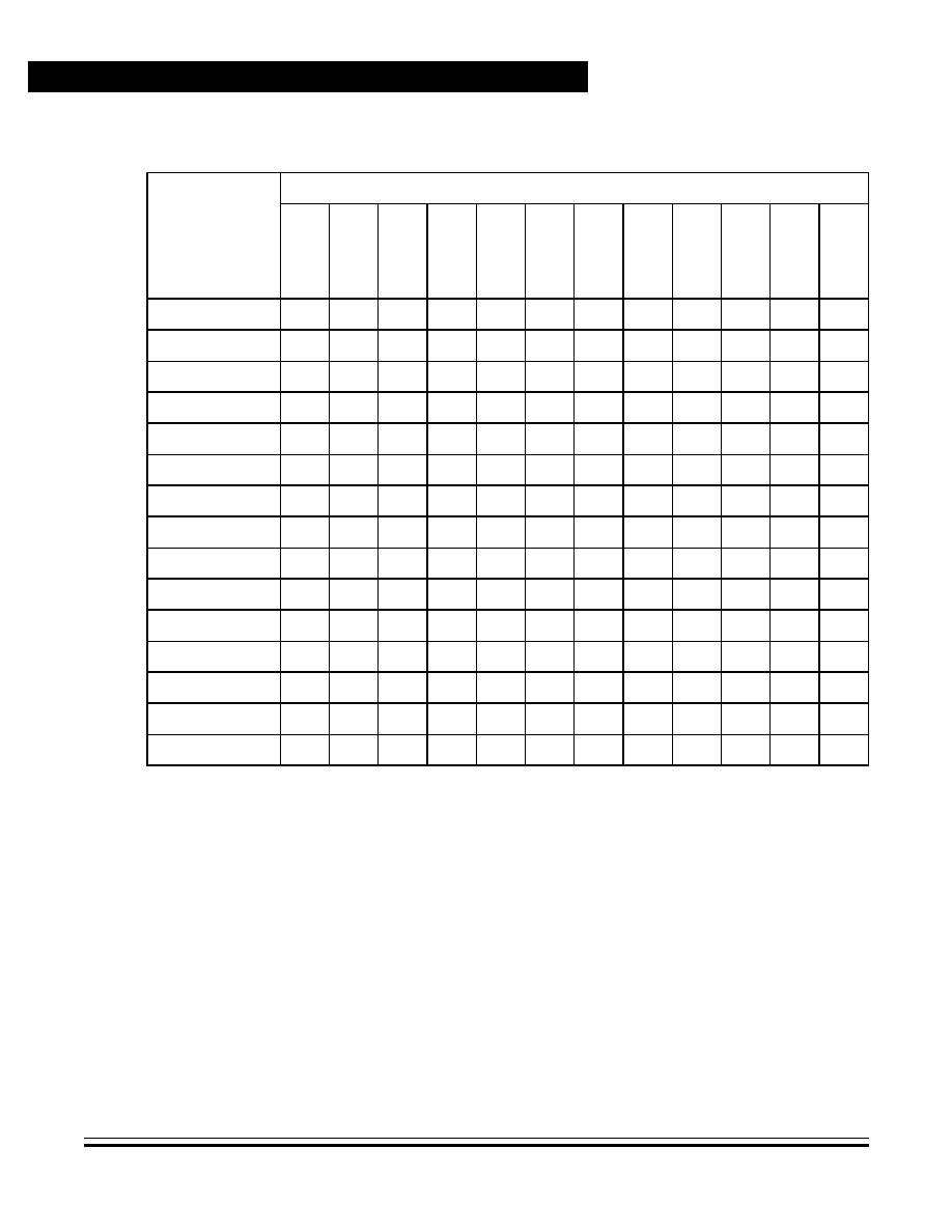
Internal Clock Generator Module (ICG)
Advance Information
MC68HC908RK2
--
Rev. 4.0
138
Internal Clock Generator Module (ICG)
MOTOROLA
Table 8-5. ICG Module Register Bit Interaction Summary
Condition
Register Bit Results for Given Condition
CM
I
E
CM
F
CM
O
N
CS
I
C
GON
IC
G
S
E
C
GON
EC
G
S
N[6:0]
T
R
I
M
[7:0]
DD
I
V
[3:0]
DS
T
G
[7:0]
Reset
0
0
0
0
1
0
0
0
$15
$80
--
--
CMF = 1
--
(1)
1
--
1
--
1
--
uw
uw
uw
uw
CMON = 0
0
0
(0)
--
--
--
--
--
--
--
--
--
CMON = 1
--
--
(1)
--
1
--
1
--
uw
uw
uw
uw
CS = 0
--
--
--
(0)
1
--
--
--
--
--
uw
uw
CS = 1
--
--
--
(1)
--
--
1
--
--
--
--
--
ICGON = 0
0
0
0
1
(0)
0
1
--
--
--
--
--
ICGON = 1
--
--
--
--
(1)
--
--
--
--
--
uw
uw
ICGS = 0
us
--
us
uc
--
(0)
--
--
--
--
--
--
ECGON = 0
0
0
0
0
1
--
(0)
0
--
--
uw
uw
ECGS = 0
us
--
us
us
--
--
--
(0)
--
--
--
--
IOFF = 1
--
1*
(1)
1
(1)
0
(1)
--
uw
uw
uw
uw
EOFF = 1
--
1*
(1)
0
(1)
--
(1)
0
uw
uw
uw
uw
N = written
(0)
(0)
(0)
--
--
0*
--
--
--
--
--
--
TRIM = written
(0)
(0)
(0)
--
--
0*
--
--
--
--
--
--
--
Register bit is unaffected by the given condition.
0, 1
Register bit is forced clear or set, respectively, in the given condition.
0*, 1*
Register bit is temporarily forced clear or set, respectively, in the given condition.
(0), (1)
Register bit must be clear or set, respectively, for the given condition to occur.
us, uc, uw
Register bit cannot be set, cleared, or written, respectively, in the given condition.
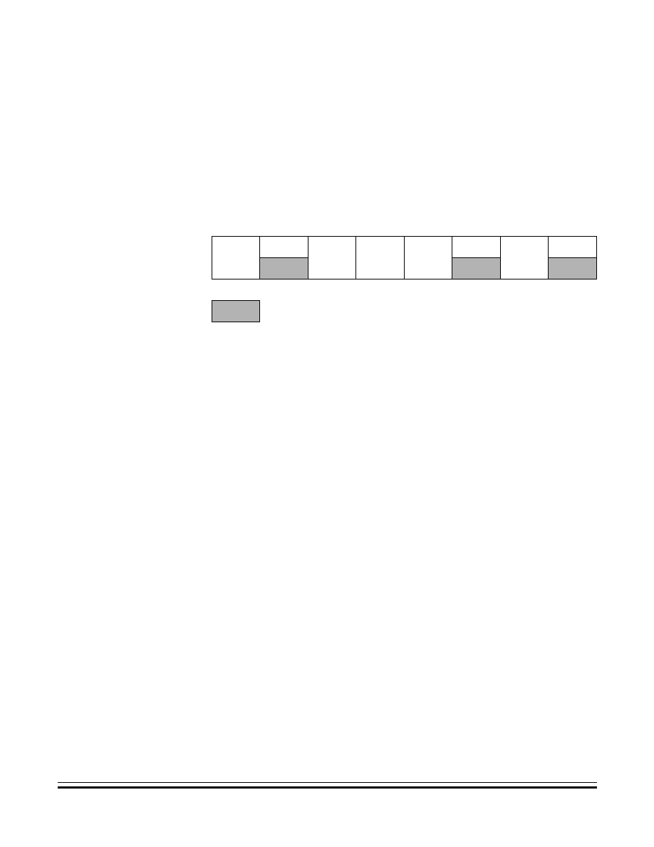
Internal Clock Generator Module (ICG)
I/O Registers
MC68HC908RK2
--
Rev. 4.0
Advance Information
MOTOROLA
Internal Clock Generator Module (ICG)
139
8.8.1 ICG Control Register
The ICG control register (ICGCR) contains the control and status bits for
the internal clock generator, external clock generator, and clock monitor
as well as the clock select and interrupt enable bits.
CMIE -- Clock Monitor Interrupt Enable Bit
This read/write bit enables clock monitor interrupts. An interrupt will
occur when both CMIE and CMF are set. CMIE can be set when the
CMON bit has been set for at least one cycle. CMIE is forced clear
when CMON is clear or during reset.
1 = Clock monitor interrupts enabled
0 = Clock monitor interrupts disabled
CMF -- Clock Monitor Interrupt Flag
This read-only bit is set when the clock monitor determines that either
ICLK or ECLK becomes inactive and the CMON bit is set. This bit is
cleared by first reading the bit while it is set, followed by writing the bit
low. This bit is forced clear when CMON is clear or during reset.
1 = Either ICLK or ECLK has become inactive.
0 = ICLK and ECLK have not become inactive since the last read
of the ICGCR or the clock monitor is disabled.
CMON -- Clock Monitor On Bit
This read/write bit enables the clock monitor. CMON can be set when
both ICLK and ECLK have been on and stable for at least one bus
cycle (ICGON, ECGON, ICGS, and ECGS are all set). CMON is
Address: $0036
Bit 7
6
5
4
3
2
1
Bit 0
Read:
CMIE
CMF
CMON
CS
ICGON
ICGS
ECGON
ECGS
Write:
Reset:
0
0
0
0
1
0
0
0
= Unimplemented
Figure 8-11. ICG Control Register (ICGCR)

Internal Clock Generator Module (ICG)
Advance Information
MC68HC908RK2
--
Rev. 4.0
140
Internal Clock Generator Module (ICG)
MOTOROLA
forced set when CMF is set, to avoid inadvertent clearing of CMF.
CMON is forced clear when either ICGON or ECGON is clear or
during reset.
1 = Clock monitor output enabled
0 = Clock monitor output disabled
CS -- Clock Select Bit
This read/write bit determines which clock will generate the oscillator
output clock (CGMXCLK). This bit can be set when ECGON and
ECGS have been set for at least one bus cycle and can be cleared
when ICGON and ICGS have been set for at least one bus cycle. This
bit is forced set when the clock monitor determines the internal clock
(ICLK) is inactive or when ICGON is clear. This bit is forced clear
when the clock monitor determines that the external clock (ECLK) is
inactive, when ECGON is clear, or during reset.
1 = External clock (ECLK) sources CGMXCLK
0 = Internal clock (ICLK) sources CGMXCLK
ICGON -- Internal Clock Generator On Bit
This read/write bit enables the internal clock generator. ICGON can
be cleared when the CS bit has been set and the CMON bit has been
clear for at least one bus cycle. ICGON is forced set when the CMON
bit is set, the CS bit is clear, or during reset.
1 = Internal clock generator enabled
0 = Internal clock generator disabled
ICGS -- Internal Clock Generator Stable Bit
This read-only bit indicates when the internal clock generator has
determined that the internal clock (ICLK) is within about 5 percent of
the desired value. This bit is forced clear when the clock monitor
determines the ICLK is inactive, when ICGON is clear, when the ICG
multiplier factor is written, or during reset.
1 = Internal clock is within 5 percent of the desired value.
0 = Internal clock may not be within 5 percent of the desired value.

Internal Clock Generator Module (ICG)
I/O Registers
MC68HC908RK2
--
Rev. 4.0
Advance Information
MOTOROLA
Internal Clock Generator Module (ICG)
141
ECGON -- External Clock Generator On Bit
This read/write bit enables the external clock generator. ECGON can
be cleared when the CS and CMON bits have been clear for at least
one bus cycle. ECGON is forced set when the CMON bit or the CS bit
is set. ECGON is forced clear during reset.
1 = External clock generator enabled
0 = External clock generator disabled
ECGS -- External Clock Generator Stable Bit
This read-only bit indicates when at least 4096 external clock (ECLK)
cycles have elapsed since the external clock generator was enabled.
This is not an assurance of the stability of ECLK but is meant to
provide a start-up delay. This bit is forced clear when the clock
monitor determines ECLK is inactive, when ECGON is clear, or during
reset.
1 = 4096 ECLK cycles have elapsed since ECGON was set.
0 = External cock is unstable, inactive, or disabled.
8.8.2 ICG Multiplier Register
N6≠N0 -- ICG Multiplier Factor Bits
These read/write bits change the multiplier used by the internal clock
generator. The internal clock (ICLK) will be (307.2 kHz
±
25
percent) * N. A value of $00 in this register is interpreted the same as
a value of $01. This register cannot be written when the CMON bit is
set. Reset sets this factor to $15 (decimal 21) for default frequency of
6.45 MHz
±
25 percent (1.613 MHz
±
25 percent bus).
Address: $0037
Bit 7
6
5
4
3
2
1
Bit 0
Read:
R
N6
N5
N4
N3
N2
N1
N0
Write:
Reset:
0
0
0
1
0
1
0
1
R
= Reserved
Figure 8-12. ICG Multiplier Register (ICGMR)

Internal Clock Generator Module (ICG)
Advance Information
MC68HC908RK2
--
Rev. 4.0
142
Internal Clock Generator Module (ICG)
MOTOROLA
8.8.3 ICG Trim Register
TRIM7≠TRIM0 -- ICG Trim Factor Bits
These read/write bits change the size of the internal capacitor used
by the internal clock generator. By testing the frequency of the internal
clock and incrementing or decrementing this factor accordingly, the
accuracy of the internal clock can be improved to
±
2 percent.
Incrementing this register by one decreases the frequency by
0.195 percent of the unadjusted value. Decrementing this register by
one increases the frequency by 0.195 percent. This register cannot
be written when the CMON bit is set. Reset sets these bits to $80,
centering the range of possible adjustment.
NOTE:
It is recommended that the user preserve a copy of the contents of the
ICG trim register (ICGTR) in non-volitale memory.
Address $7FEF is reserved for an optional factory-determined ICG trim
value. Consult with a local Motorola representative for more information
and availability of this option.
Address: $0038
Bit 7
6
5
4
3
2
1
Bit 0
Read:
TRIM7
TRIM6
TRIM5
TRIM4
TRIM3
TRIM2
TRIM1
TRIM0
Write:
Reset:
1
0
0
0
0
0
0
0
Figure 8-13. ICG Trim Register (ICGTR)

Internal Clock Generator Module (ICG)
I/O Registers
MC68HC908RK2
--
Rev. 4.0
Advance Information
MOTOROLA
Internal Clock Generator Module (ICG)
143
8.8.4 ICG DCO Divider Register
DDIV3≠DDIV0 -- ICG DCO Divider Control Bits
These bits indicate the number of divide-by-twos (DDIV) that follow
the digitally controlled oscillator. Incrementing DDIV will add another
divide-by-two, doubling the period (halving the frequency).
Decrementing has the opposite effect. DDIV cannot be written when
ICGON is set to prevent inadvertent frequency shifting. When ICGON
is set, DDIV is controlled by the digital loop filter. The range of valid
values for DDIV is from $0 to $9. Values of $A≠$F are interpreted the
same as $9. Since the DCO is active during reset, reset has no effect
on DSTG and the value may vary.
Address: $0039
Bit 7
6
5
4
3
2
1
Bit 0
Read:
R
R
R
R
DDIV3
DDIV2
DDIV1
DDIV0
Write:
Reset:
0
0
0
0
U
U
U
U
R
= Reserved
U = Unaffected
Figure 8-14. ICG DCO Divider Register (ICGDVR)
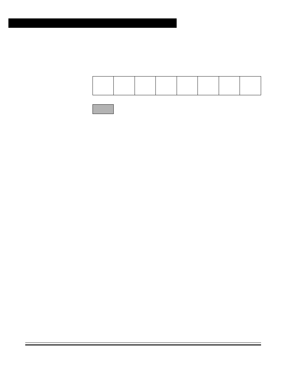
Internal Clock Generator Module (ICG)
Advance Information
MC68HC908RK2
--
Rev. 4.0
144
Internal Clock Generator Module (ICG)
MOTOROLA
8.8.5 ICG DCO Stage Register
DSTG7≠DSTG0 -- ICG DCO Stage Control Bits
These bits indicate the number of stages DSTG (above the minimum)
in the digitally controlled oscillator. The total number of stages is
approximately equal to $1FF, so changing DSTG from $00 to $FF will
approximately double the period. Incrementing DSTG will increase
the period (decrease the frequency) by 0.202 percent to 0.368
percent (decrementing has the opposite effect). DSTG cannot be
written when ICGON is set to prevent inadvertent frequency shifting.
When ICGON is set, DSTG is controlled by the digital loop filter. Since
the DCO is active during reset, reset has no effect on DSTG and the
value may vary.
Address: $003A
Bit 7
6
5
4
3
2
1
Bit 0
Read:
DSTG7
DSTG6
DSTG5
DSTG4
DSTG3
DSTG2
DSTG1
DSTG0
Write:
Reset:
Unaffected by reset
= Unimplemented
Figure 8-15. ICG DCO Stage Register (ICGDSR)

MC68HC908RK2
--
Rev. 4.0
Advance Information
MOTOROLA
Configuration Register (CONFIG)
145
Advance Information -- MC68HC908RK2
Section 9. Configuration Register (CONFIG)
9.1 Contents
9.2
Introduction . . . . . . . . . . . . . . . . . . . . . . . . . . . . . . . . . . . . . . . 145
9.3
Functional Description . . . . . . . . . . . . . . . . . . . . . . . . . . . . . . 145
9.2 Introduction
This section describes the configuration register (CONFIG). The
configuration register enables or disables these options:
∑
Stop mode recovery time (32 CGMXCLK cycles or 4,096
CGMXCLK cycles)
∑
COP timeout period (2
18
≠ 2
4
or 2
13
≠ 2
4
CGMXCLK cycles)
∑
STOP instruction
∑
Computer operating properly module (COP)
∑
Low-voltage inhibit (LVI) module control
9.3 Functional Description
The CONFIG register is used in the initialization of various options and
can be written once after each reset. The register is set to the
documented value during reset. Since the various options affect the
operation of the MCU, it is recommended that these registers be written
immediately after reset. The configuration register is located at $001F.
NOTE:
On a FLASH device, the options are one-time writable by the user after
each reset. The CONFIG register is not in the FLASH memory but is a
special register containing one-time writable latches after each reset.

Configuration Register (CONFIG)
Advance Information
MC68HC908RK2
--
Rev. 4.0
146
Configuration Register (CONFIG)
MOTOROLA
Upon a reset, the CONFIG register defaults to predetermined settings as
shown in
Figure 2-1. Memory Map
.
EXTSLOW -- Slow External Crystal Enable Bit
The EXTSLOW bit has two functions. It configures the ICG module for
a fast (1 MHz≠8 MHz) or slow (30 kHz≠100 kHz) speed crystal. The
option also configures the clock monitor operation in the ICG module
to expect an external frequency higher (307.2 kHz≠32 MHz) or lower
(60 Hz≠307.2 kHz) than the base frequency of the internal oscillator.
(See
Section 8. Internal Clock Generator Module (ICG)
.)
1 = ICG set for slow external crystal operation
0 = ICG set for fast external crystal operation
LVISTOP -- LVI Enable in Stop Mode Bit
When the LVIPWR bit is set, setting the LVISTOP bit enables the LVI
to operate during stop mode. Reset clears LVISTOP.
1 = LVI enabled during stop mode
0 = LVI disabled during stop mode
LVIRST -- LVI Reset Enable Bit
LVIRST enables the reset signal from the LVI module.
(See
Section 12. Low-Voltage Inhibit (LVI)
.)
1 = LVI module resets enabled
0 = LVI module resets disabled
LVIPWR -- LVI Power Enable Bit
LVIPWR disables the LVI module. (See
Section 12. Low-Voltage
Inhibit (LVI)
.)
1 = LVI module power enabled
0 = LVI module power disabled
Address:
$001F
BIt 7
6
5
4
3
2
1
Bit 0
Read:
EXTSLOW LVISTOP
LVIRST
LVIPWR
COPRS
SSREC
STOP
COPD
Write:
Reset:
0
0
1
1
0
0
0
0
Figure 9-1. Configuration Register (CONFIG)

Configuration Register (CONFIG)
Functional Description
MC68HC908RK2
--
Rev. 4.0
Advance Information
MOTOROLA
Configuration Register (CONFIG)
147
COPRS -- COP Rate Select Bit
COPRS selects the COP timeout period. Reset clears COPRS. (See
Section 11. Computer Operating Properly Module (COP)
.)
1 = COP timeout period = 2
13
≠ 2
4
CGMXCLK cycles
0 = COP timeout period = 2
18
≠ 2
4
CGMXCLK cycles
SSREC -- Short Stop Recovery Bit
SSREC enables the CPU to exit stop mode with a delay of 32
CGMXCLK cycles instead of a 4096-CGMXCLK cycle delay.
1 = Stop mode recovery after 32 CGMXCLK cycles
0 = Stop mode recovery after 4096 CGMXCLK cycles
NOTE:
Exiting stop mode by pulling reset will result in the long stop recovery.
If using the internal clock generator module or an external crystal
oscillator, do not set the SSREC bit.
The LVI has an enable time of t
en
. The system stabilization time for
power-on reset and long stop recovery (both 4096 CGMXCLK cycles)
gives a delay longer than the LVI enable time for these startup scenarios.
There is no period where the MCU is not protected from a low power
condition. However, when using the short stop recovery configuration
option, the 32 CGMXCLK delay must be greater than the LVI's turn on
time to avoid a period in startup where the LVI is not protecting the MCU.
STOP -- STOP Instruction Enable Bit
STOP enables the STOP instruction.
1 = STOP instruction enabled
0 = STOP instruction treated as illegal opcode
COPD -- COP Disable Bit
COPD disables the COP module. (See
Section 11. Computer
Operating Properly Module (COP)
.)
1 = COP module disabled
0 = COP module enabled

Configuration Register (CONFIG)
Advance Information
MC68HC908RK2
--
Rev. 4.0
148
Configuration Register (CONFIG)
MOTOROLA

MC68HC908RK2
--
Rev. 4.0
Advance Information
MOTOROLA
Monitor Read-Only Memory (MON)
149
Advance Information -- MC68HC908RK2
Section 10. Monitor Read-Only Memory (MON)
10.1 Contents
10.2
Introduction . . . . . . . . . . . . . . . . . . . . . . . . . . . . . . . . . . . . . . . 149
10.3
Features . . . . . . . . . . . . . . . . . . . . . . . . . . . . . . . . . . . . . . . . . 150
10.4
Functional Description . . . . . . . . . . . . . . . . . . . . . . . . . . . . . . 150
10.4.1
Monitor Mode Entry . . . . . . . . . . . . . . . . . . . . . . . . . . . . . . 152
10.4.2
Data Format . . . . . . . . . . . . . . . . . . . . . . . . . . . . . . . . . . . . 153
10.4.3
Echoing . . . . . . . . . . . . . . . . . . . . . . . . . . . . . . . . . . . . . . . 154
10.4.4
Break Signal . . . . . . . . . . . . . . . . . . . . . . . . . . . . . . . . . . . . 154
10.4.5
Commands . . . . . . . . . . . . . . . . . . . . . . . . . . . . . . . . . . . . .155
10.4.6
Baud Rate . . . . . . . . . . . . . . . . . . . . . . . . . . . . . . . . . . . . .158
10.4.7
Security . . . . . . . . . . . . . . . . . . . . . . . . . . . . . . . . . . . . . . . 158
10.2 Introduction
This section describes the monitor read-only memory (MON). The MON
allows complete testing of the MCU through a single-wire interface with
a host computer.

Monitor Read-Only Memory (MON)
Advance Information
MC68HC908RK2
--
Rev. 4.0
150
Monitor Read-Only Memory (MON)
MOTOROLA
10.3 Features
Features of the monitor ROM include:
∑
Normal user-mode pin functionality
∑
One pin dedicated to serial communication between monitor ROM
and host computer
∑
Standard mark/space non-return-to-zero (NRZ) communication
with host computer
∑
9600 baud communication with host computer when using a
9.8304-MHz crystal
∑
Execution of code in random-access memory (RAM) or FLASH
∑
FLASH security
∑
FLASH programming
10.4 Functional Description
Monitor ROM receives and executes commands from a host computer.
Figure 10-1
shows a sample circuit used to enter monitor mode and
communicate with a host computer via a standard RS-232 interface.
While simple monitor commands can access any memory address, the
MC68HC908RK2 has a FLASH security feature to prevent external
viewing of the contents of FLASH. Proper procedures must be followed
to verify FLASH content. Access to the FLASH is denied to unauthorized
users of customer-specified software (see
10.4.7 Security
).
In monitor mode, the MCU can execute host-computer code in RAM
while all MCU pins except PTA0 retain normal operating mode functions.
All communication between the host computer and the MCU is through
the PTA0 pin. A level-shifting and multiplexing interface is required
between PTA0 and the host computer. PTA0 is used in a wired-OR
configuration and requires a pullup resistor.
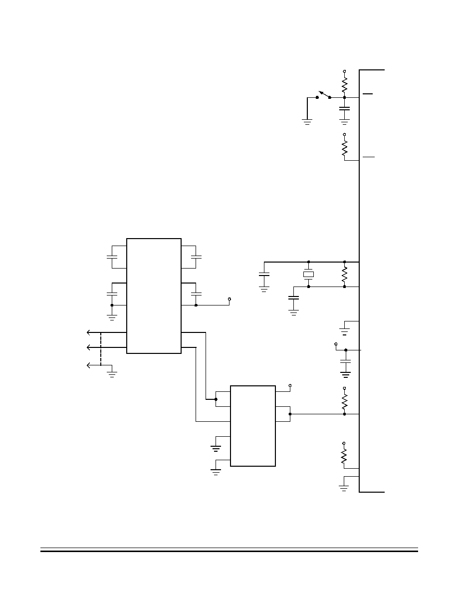
Monitor Read-Only Memory (MON)
Functional Description
MC68HC908RK2
--
Rev. 4.0
Advance Information
MOTOROLA
Monitor Read-Only Memory (MON)
151
Figure 10-1. Monitor Mode Circuit
+
+
+
10 M
X1
V
DD
V
HI
MC145407
MC74HC125
68HC908RK2
RST
IRQ1
OSC1
OSC2
V
SS
V
DD
PTA0
V
DD
10 k
0.1
µ
F
10 k
6
5
2
4
3
1
DB-25
2
3
7
20
18
17
19
16
15
V
DD
V
DD
V
DD
20 pF
20 pF
10
µ
F
10
µ
F
10
µ
F
10
µ
F
1
2
4
7
14
3
0.1
µ
F
9.8304 MHz
10 k
10 k
5
6
+
PTB0
PTB2
V
DD
10 k

Monitor Read-Only Memory (MON)
Advance Information
MC68HC908RK2
--
Rev. 4.0
152
Monitor Read-Only Memory (MON)
MOTOROLA
10.4.1 Monitor Mode Entry
Table 10-1
shows the pin conditions for entering monitor mode.
Enter monitor mode by either:
∑
Executing a software interrupt instruction (SWI), or
∑
Applying a logic 0 and then a logic 1 to the RST pin
NOTE:
Upon entering monitor mode, an interrupt stack frame plus a stacked H
register will leave the stack pointer at address $00F9.
Once out of reset, the MCU waits for the host to send eight security bytes
(see
10.4.7 Security
). After the security bytes, the MCU sends a break
signal (10 consecutive logic 0s) to the host computer, indicating that it is
ready to receive a command.
Monitor mode uses alternate vectors for reset, SWI, and break interrupt.
The alternate vectors are in the $FE page instead of the $FF page and
allow code execution from the internal monitor firmware instead of user
code. The COP module is disabled in monitor mode as long as V
HI
(see
Section 16. Preliminary Electrical Specifications
) is applied to either
the IRQ1 pin or the RST pin. (See
Section 6. System Integration
Module (SIM)
for more information on modes of operation.) The ICG
module is bypassed in monitor mode as long as V
HI
is applied to the
IRQ1 pin. RST does not affect the ICG.
Table 10-1. Monitor Mode Entry
IR
Q
Pi
n
PT
B
0
Pin
PT
B
2
Pin
PT
A
0
Pin
CGMOUT
(2)
Bus
Frequency
V
HI
(1)
1
0
1
1. For V
HI
, see
16.7 3.0-Volt DC Electrical Characteristics
and
16.3 Absolute Maximum
Ratings
.
2. If the high voltage (V
HI
) is removed from the IRQ1 pin while in monitor mode, the clock
select bit (CS) controls the source of CGMOUT.
CGMXCLK
2
-----------------------------
CGMOUT
2
--------------------------
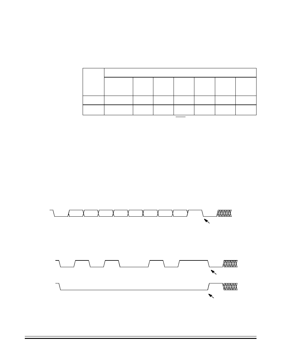
Monitor Read-Only Memory (MON)
Functional Description
MC68HC908RK2
--
Rev. 4.0
Advance Information
MOTOROLA
Monitor Read-Only Memory (MON)
153
Table 10-2
is a summary of the differences between user mode and
monitor mode.
10.4.2 Data Format
Communication with the monitor ROM is in standard non-return-to-zero
(NRZ) mark/space data format. (See
Figure 10-2
and
Figure 10-3
.)
The data transmit and receive rate is determined by the crystal. Transmit
and receive baud rates must be identical.
Figure 10-2. Monitor Data Format
Figure 10-3. Sample Monitor Waveforms
Table 10-2. Mode Differences
Modes
Functions
COP
Reset
Vector
High
Reset
Vector
Low
Break
Vector
High
Break
Vector
Low
SWI
Vector
High
SWI
Vector
Low
User
Enabled
$FFFE
$FFFF
$FFFC
$FFFD
$FFFC
$FFFD
Monitor
Disabled
(1)
1. If the high voltage (V
HI
) is removed from the IRQ1 pin while in monitor mode, the SIM
asserts its COP enable output. The COP is a mask option enabled or disabled by the
COPD bit in the configuration register. See
16.7 3.0-Volt DC Electrical Characteristics
.
$FEFE
$FEFF
$FEFC
$FEFD
$FEFC
$FEFD
BIT 5
START
BIT
BIT 0
BIT 1
NEXT
STOP
BIT
START
BIT
BIT 2
BIT 3
BIT 4
BIT 6
BIT 7
Notes: 1 = Echo delay (2 bit times)
2 = Data return delay (2 bit times)
3 = Wait 1 bit time before sending next byte.
1, 2, 3
BIT 5
START
BIT
BIT 0
BIT 1
NEXT
STOP
BIT
START
BIT
BIT 2
BIT 3
BIT 4
BIT 6
BIT 7
START
BIT
BIT 0
BIT 1
NEXT
STOP
BIT
START
BIT
BIT 2
$A5
BREAK
BIT 3
BIT 4
BIT 5
BIT 6
BIT 7
Notes: 1 = Echo delay (2 bit times)
2 = Data return delay (2 bit times)
3 = Wait 1 bit time before sending next byte.
1, 2, 3
1, 2, 3
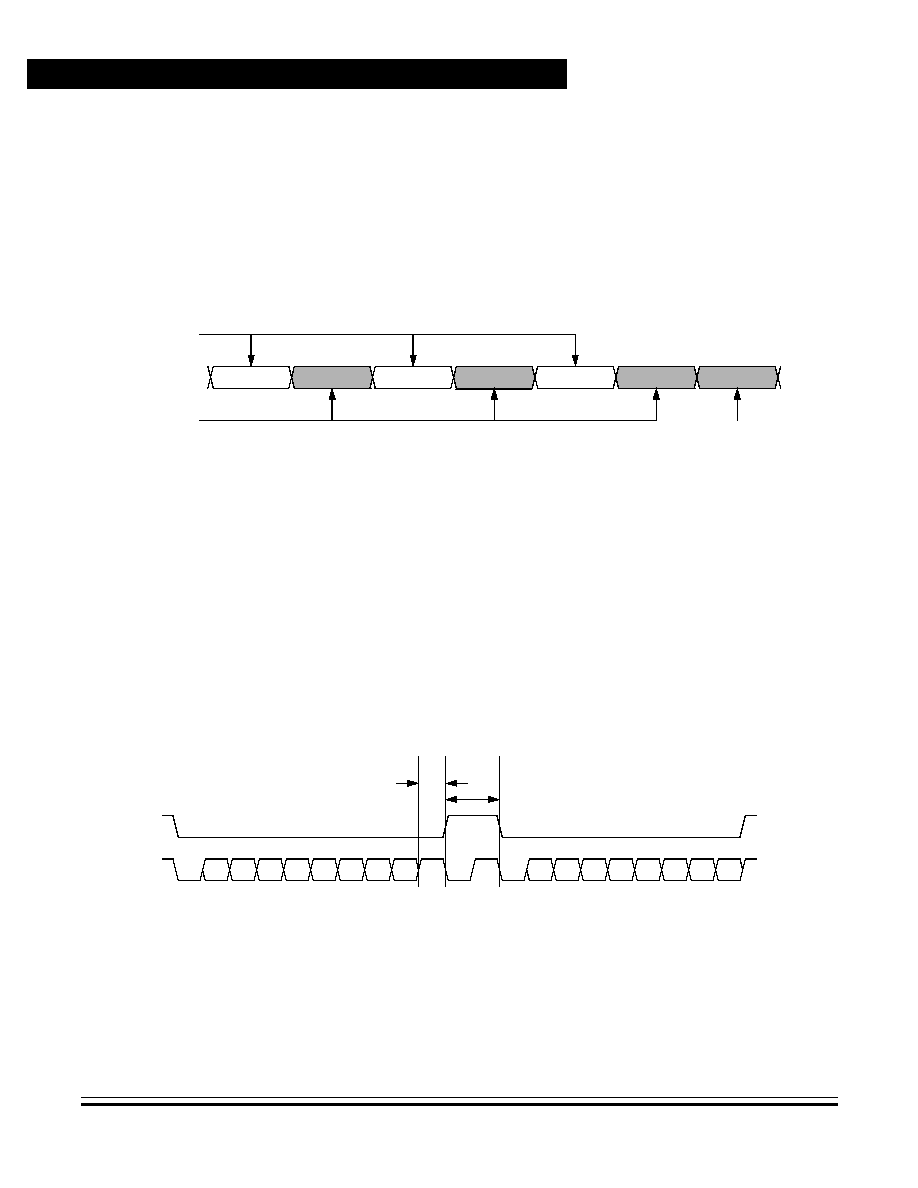
Monitor Read-Only Memory (MON)
Advance Information
MC68HC908RK2
--
Rev. 4.0
154
Monitor Read-Only Memory (MON)
MOTOROLA
10.4.3 Echoing
As shown in
Figure 10-4
, the monitor ROM immediately echoes each
received byte back to the PTA0 pin for error checking.
Any result of a command appears after the echo of the last byte of the
command.
Figure 10-4. Read Transaction
10.4.4 Break Signal
A start bit followed by nine low bits is a break signal. (See
Figure 10-5
.)
When the monitor receives a break signal, it drives the PTA0 pin high for
the duration of two bits before echoing the break signal.
Figure 10-5. Break Transaction
ADDR. HIGH
READ
READ
ADDR. HIGH
ADDR. LOW
ADDR. LOW
DATA
ECHO
SENT TO
MONITOR
RESULT
Notes: 1 = Echo delay (2 bit times)
2 = Data return delay (2 bit times)
3 = Wait 1 bit time before sending next byte.
1
3
1
3
1
2
0
1
2
3
4
5
6
7
0
1
2
3
4
5
6
7
MISSING STOP BIT
2-STOP-BIT DELAY BEFORE ZERO ECHO
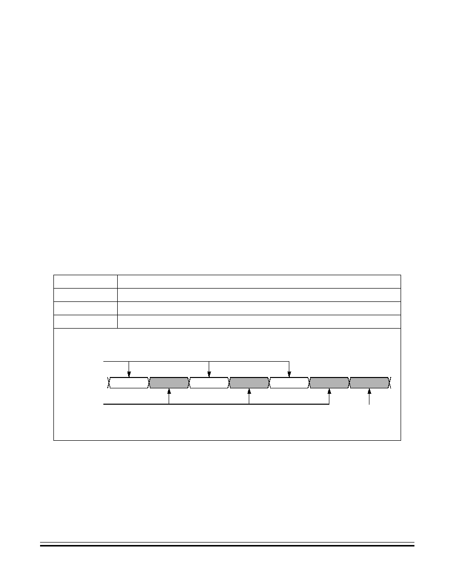
Monitor Read-Only Memory (MON)
Functional Description
MC68HC908RK2
--
Rev. 4.0
Advance Information
MOTOROLA
Monitor Read-Only Memory (MON)
155
10.4.5 Commands
The monitor ROM uses these commands:
∑
READ, read memory
∑
WRITE, write memory
∑
IREAD, indexed read
∑
IWRITE, indexed write
∑
READSP, read stack pointer
∑
RUN, run user program
A sequence of IREAD or IWRITE commands can access a block of
memory sequentially over the full 64-Kbyte memory map.
Table 10-3. READ (Read Memory) Command
Description
Read byte from memory
Operand
Specifies 2-byte address in high byte:low byte order
Data Returned
Returns contents of specified address
Opcode
$4A
Command Sequence
ADDR. HIGH
READ
READ
ADDR. HIGH
ADDR. LOW
ADDR. LOW
DATA
ECHO
SENT TO
MONITOR
RESULT
Notes: 1 = Echo delay (2 bit times)
2 = Data return delay (2 bit times)
3 = Wait 1 bit time before sending next byte.
1
3
1
3
1
2
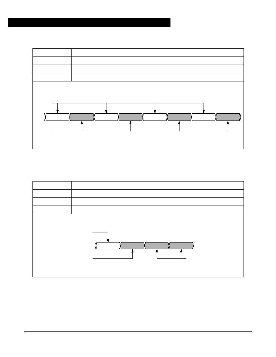
Monitor Read-Only Memory (MON)
Advance Information
MC68HC908RK2
--
Rev. 4.0
156
Monitor Read-Only Memory (MON)
MOTOROLA
Table 10-4. WRITE (Write Memory) Command
Description
Write byte to memory
Operand
Specifies 2-byte address in high byte:low byte order; low byte followed by data byte
Data Returned
None
Opcode
$49
Command Sequence
ADDR. HIGH
WRITE
WRITE
ADDR. HIGH
ADDR. LOW
ADDR. LOW
DATA
ECHO
SENT TO
MONITOR
DATA
Notes: 1 = Echo delay (2 bit times)
2 = Wait 1 bit time before sending next byte.
1
2
1
2
1
2
1
Table 10-5. IREAD (Indexed Read) Command
Description
Read next 2 bytes in memory from last address accessed
Operand
Specifies 2-byte address in high byte:low byte order
Data Returned
Returns contents of next two addresses
Opcode
$1A
Command Sequence
DATA
IREAD
IREAD
DATA
ECHO
SENT TO
MONITOR
RESULT
Notes: 1 = Echo delay (2 bit times)
2 = Data return delay (2 bit times)
1
2
2
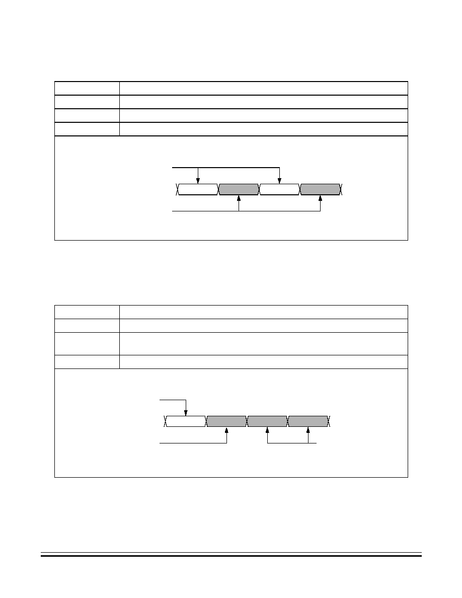
Monitor Read-Only Memory (MON)
Functional Description
MC68HC908RK2
--
Rev. 4.0
Advance Information
MOTOROLA
Monitor Read-Only Memory (MON)
157
Table 10-6. IWRITE (Indexed Write) Command
Description
Write to last address accessed + 1
Operand
Specifies single data byte
Data Returned
None
Opcode
$19
Command Sequence
DATA
IWRITE
IWRITE
DATA
ECHO
SENT TO
MONITOR
Notes: 1 = Echo delay (2 bit times)
2 = Wait 1 bit time before sending next byte.
1
2
1
Table 10-7. READSP (Read Stack Pointer) Command
Description
Reads stack pointer
Operand
None
Data Returned
Returns stack pointer plus one in high byte:low byte order. The plus one is due to
the use of the TSX instruction.
Opcode
$0C
Command Sequence
SP HIGH
READSP
READSP
SP LOW
ECHO
SENT TO
MONITOR
RESULT
Notes: 1 = Echo delay (2 bit times)
2 = Data return delay (2 bit times)
1
2
2

Monitor Read-Only Memory (MON)
Advance Information
MC68HC908RK2
--
Rev. 4.0
158
Monitor Read-Only Memory (MON)
MOTOROLA
10.4.6 Baud Rate
With a 9.8304-MHz crystal, data is transferred between the monitor and
host at 9600 baud. If a 14.7456-MHz crystal is used, the monitor baud
rate is 14400.
NOTE:
While in monitor mode with V
HI
applied to IRQ1, the MCU bus clock is
always driven from the external clock.
10.4.7 Security
A security feature discourages unauthorized reading of FLASH locations
while in monitor mode. The host can bypass the security feature at
monitor mode entry by sending eight consecutive security bytes that
match the bytes at locations $FFF6≠$FFFD. Locations $FFF6≠$FFFD
contain user-defined data.
NOTE:
Do not leave locations $FFF6≠$FFFD blank. For security reasons,
program locations $FFF6≠$FFFD even if they are not used for vectors.
If FLASH is unprogrammed, the eight security byte values to be sent are
$00, the unprogrammed state of the FLASH.
During monitor mode entry, the MCU waits after the power-on reset for
the host to send the eight security bytes on pin PA0.
Table 10-8. RUN (Run User Program) Command
Description
Executes RTI instruction
Operand
None
Data Returned
None
Opcode
$28
Command Sequence
RUN
RUN
ECHO
SENT TO
MONITOR
Note 1 = Echo delay (2 bit times)
1
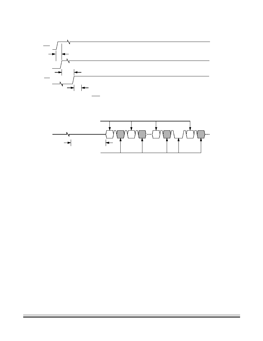
Monitor Read-Only Memory (MON)
Functional Description
MC68HC908RK2
--
Rev. 4.0
Advance Information
MOTOROLA
Monitor Read-Only Memory (MON)
159
Figure 10-6. Monitor Mode Entry Timing
If the received bytes match those at locations $FFF6≠$FFFD, the host
bypasses the security feature and can read all FLASH locations and
execute code from FLASH. Security remains bypassed until a power-on
reset occurs. After the host bypasses security, any reset other than a
power-on reset requires the host to send another eight bytes, but
security remains bypassed regardless of the data that the host sends.
If the received bytes do not match the data at locations $FFF6≠$FFFD,
the host fails to bypass the security feature. The MCU remains in monitor
mode, but reading FLASH locations returns undefined data, and trying
to execute code from FLASH causes an illegal address reset. After the
host fails to bypass security, any reset other than a power-on reset
causes an endless loop of illegal address resets.
BYT
E 1
BYT
E 1 EC
H
O
BYT
E 2
BYT
E 2 EC
H
O
BYT
E 8
BYT
E 8 EC
H
O
CO
MM
A
N
D
CO
MMA
ND
E
CHO
PA0
RST
4096 + 32 CGMXCLK CYCLES
24 CGMXCLK CYCLES
1
3
1
1
2
1
BR
EAK
Notes: 1 = Echo delay (2 bit times)
2 = Data return delay (2 bit times)
3 = Wait 1 bit time before sending next byte.
3
FROM HOST
FROM MCU
(
$
FF
F6
)
(
$
FF
F7
)
(
$
FF
FD)
256 CGMXCLK CYCLES
(ONE BIT TIME)
V
DD
IRQ1
SEE NOTE
Note: Any delay between rising IRQ1 and rising V
DD
will guarantee that the MCU bus is driven by the external clock.

Monitor Read-Only Memory (MON)
Advance Information
MC68HC908RK2
--
Rev. 4.0
160
Monitor Read-Only Memory (MON)
MOTOROLA
After receiving the eight security bytes from the host, the MCU transmits
a break character signalling that it is ready to receive a command.
NOTE:
The MCU does not transmit a break character until after the host sends
the eight security bytes.

MC68HC908RK2
--
Rev. 4.0
Advance Information
MOTOROLA
Computer Operating Properly Module (COP)
161
Advance Information -- MC68HC908RK2
Section 11. Computer Operating Properly Module (COP)
11.1 Contents
11.2
Introduction . . . . . . . . . . . . . . . . . . . . . . . . . . . . . . . . . . . . . . . 162
11.3
Functional Description . . . . . . . . . . . . . . . . . . . . . . . . . . . . . . 162
11.4
I/O Signals . . . . . . . . . . . . . . . . . . . . . . . . . . . . . . . . . . . . . . . 163
11.4.1
CGMXCLK . . . . . . . . . . . . . . . . . . . . . . . . . . . . . . . . . . . . .163
11.4.2
STOP Instruction . . . . . . . . . . . . . . . . . . . . . . . . . . . . . . . .163
11.4.3
COPCTL Write . . . . . . . . . . . . . . . . . . . . . . . . . . . . . . . . . . 164
11.4.4
Power-On Reset . . . . . . . . . . . . . . . . . . . . . . . . . . . . . . . . .164
11.4.5
Internal Reset . . . . . . . . . . . . . . . . . . . . . . . . . . . . . . . . . . . 164
11.4.6
Reset Vector Fetch. . . . . . . . . . . . . . . . . . . . . . . . . . . . . . . 164
11.4.7
COPD . . . . . . . . . . . . . . . . . . . . . . . . . . . . . . . . . . . . . . . . . 164
11.4.8
COPRS. . . . . . . . . . . . . . . . . . . . . . . . . . . . . . . . . . . . . . . . 164
11.5
COP Control Register . . . . . . . . . . . . . . . . . . . . . . . . . . . . . . . 165
11.6
Interrupts. . . . . . . . . . . . . . . . . . . . . . . . . . . . . . . . . . . . . . . . . 165
11.7
Monitor Mode . . . . . . . . . . . . . . . . . . . . . . . . . . . . . . . . . . . . .165
11.8
Low-Power Modes . . . . . . . . . . . . . . . . . . . . . . . . . . . . . . . . . 165
11.8.1
Wait Mode . . . . . . . . . . . . . . . . . . . . . . . . . . . . . . . . . . . . .165
11.8.2
Stop Mode . . . . . . . . . . . . . . . . . . . . . . . . . . . . . . . . . . . . .166
11.9
COP Module During Break Interrupts . . . . . . . . . . . . . . . . . . .166

Computer Operating Properly Module (COP)
Advance Information
MC68HC908RK2
--
Rev. 4.0
162
Computer Operating Properly Module (COP)
MOTOROLA
11.2 Introduction
The computer operating properly (COP) module contains a free-running
counter that generates a reset if allowed to overflow. The COP module
helps software recover from runaway code. Prevent a COP reset by
periodically clearing the COP counter.
11.3 Functional Description
Figure 11-1. COP Block Diagram
COPCTL WRITE
CGMXCLK
RESET VECTOR FETCH
RESET
RESET STATUS
INTERNAL RESET SOURCES
STOP INSTRUCTION
C
L
EAR
S
T
AG
ES
5
≠
12
C
L
E
A
R
A
L
L
ST
AG
ES
6-BIT COP COUNTER
COPD FROM CONFIG
RESET
COPCTL WRITE
CLEAR COP
COUNTER
COPRS FROM CONFIG
12-BIT COP PRESCALER
REGISTER

Computer Operating Properly Module (COP)
I/O Signals
MC68HC908RK2
--
Rev. 4.0
Advance Information
MOTOROLA
Computer Operating Properly Module (COP)
163
The COP counter is a free-running 6-bit counter preceded by a 12-bit
prescaler. If not cleared by software, the COP counter overflows and
generates an asynchronous reset after 2
13
≠ 2
4
or 2
18
≠ 2
4
CGMXCLK
cycles, depending on the state of the COP rate select bit, COPRS, in the
configuration register. When COPRS = 1, a 4.9152-MHz crystal gives a
COP timeout period of 53.3 ms. Writing any value to location $FFFF
before an overflow occurs prevents a COP reset by clearing the COP
counter and stages 5 through 12 of the prescaler.
NOTE:
Service the COP immediately after reset and before entering or after
exiting stop mode to guarantee the maximum time before the first COP
counter overflow.
A COP reset pulls the RST pin low for 32 CGMXCLK cycles and sets the
COP bit in the SIM reset status register (SRSR).
In monitor mode, the COP is disabled if the RST pin or the IRQ1 pin is
held at V
HI
. During the break state, V
HI
on the RST pin disables the COP.
NOTE:
Place COP clearing instructions in the main program and not in an
interrupt subroutine. Such an interrupt subroutine could keep the COP
from generating a reset even while the main program is not working
properly.
11.4 I/O Signals
The following paragraphs describe the signals shown in
Figure 11-1
.
11.4.1 CGMXCLK
CGMXCLK is the oscillator output signal. See
8.4.5 Clock Selection
Circuit
for a description of CGMXCLK.
11.4.2 STOP Instruction
The STOP instruction clears the COP prescaler.

Computer Operating Properly Module (COP)
Advance Information
MC68HC908RK2
--
Rev. 4.0
164
Computer Operating Properly Module (COP)
MOTOROLA
11.4.3 COPCTL Write
Writing any value to the COP control register (COPCTL) (see
11.5 COP
Control Register
), clears the COP counter and clears stages 12
through 5 of the COP prescaler. Reading the COP control register
returns the reset vector.
11.4.4 Power-On Reset
The power-on reset (POR) circuit clears the COP prescaler 4096
CGMXCLK cycles after power up.
11.4.5 Internal Reset
An internal reset clears the COP prescaler and the COP counter.
11.4.6 Reset Vector Fetch
A reset vector fetch occurs when the vector address appears on the data
bus. A reset vector fetch clears the COP prescaler.
11.4.7 COPD
The COPD signal reflects the state of the COP disable bit (COPD) in the
configuration register. (See
Section 9. Configuration Register
(CONFIG)
).
11.4.8 COPRS
The COPRS signal reflects the state of the COP rate select bit (COPRS)
in the configuration register. (See
Section 9. Configuration Register
(CONFIG)
).

Computer Operating Properly Module (COP)
COP Control Register
MC68HC908RK2
--
Rev. 4.0
Advance Information
MOTOROLA
Computer Operating Properly Module (COP)
165
11.5 COP Control Register
The COP control register is located at address $FFFF and overlaps the
reset vector. Writing any value to $FFFF clears the COP counter and
starts a new timeout period. Reading location $FFFF returns the low
byte of the reset vector.
11.6 Interrupts
The COP does not generate CPU interrupt requests.
11.7 Monitor Mode
The COP is disabled in monitor mode when V
HI
is present on the IRQ1
pin or on the RST pin.
11.8 Low-Power Modes
The WAIT and STOP instructions put the MCU in low power-
consumption standby modes.
11.8.1 Wait Mode
The COP remains active in wait mode. To prevent a COP reset during
wait mode, periodically clear the COP counter in a CPU interrupt routine.
Address:
$FFFF
Bit 7
6
5
4
3
2
1
Bit 0
Read:
Low byte of reset vector
Write:
Clear COP counter
Reset:
Unaffected by reset
Figure 11-2. COP Control Register (COPCTL)

Computer Operating Properly Module (COP)
Advance Information
MC68HC908RK2
--
Rev. 4.0
166
Computer Operating Properly Module (COP)
MOTOROLA
11.8.2 Stop Mode
Stop mode turns off the CGMXCLK input to the COP and clears the COP
prescaler. Service the COP immediately before entering or after exiting
stop mode to ensure a full COP timeout period after entering or exiting
stop mode.
The STOP bit (see
Section 9. Configuration Register (CONFIG)
)
enables the STOP instruction. To prevent inadvertently turning off the
COP with a STOP instruction, disable the STOP instruction by clearing
the STOP bit.
11.9 COP Module During Break Interrupts
The COP is disabled during a break interrupt when V
HI
is present on the
RST pin.

MC68HC908RK2
--
Rev. 4.0
Advance Information
MOTOROLA
Low-Voltage Inhibit (LVI)
167
Advance Information -- MC68HC908RK2
Section 12. Low-Voltage Inhibit (LVI)
12.1 Contents
12.2
Introduction . . . . . . . . . . . . . . . . . . . . . . . . . . . . . . . . . . . . . . . 167
12.3
Features . . . . . . . . . . . . . . . . . . . . . . . . . . . . . . . . . . . . . . . . . 168
12.4
Functional Description . . . . . . . . . . . . . . . . . . . . . . . . . . . . . . 168
12.4.1
False Trip Protection . . . . . . . . . . . . . . . . . . . . . . . . . . . . . 169
12.4.2
Short Stop Recovery Option. . . . . . . . . . . . . . . . . . . . . . . . 169
12.5
LVI Status Register. . . . . . . . . . . . . . . . . . . . . . . . . . . . . . . . .170
12.6
LVI Interrupts . . . . . . . . . . . . . . . . . . . . . . . . . . . . . . . . . . . . .170
12.7
Low-Power Modes . . . . . . . . . . . . . . . . . . . . . . . . . . . . . . . . . 170
12.7.1
Wait Mode . . . . . . . . . . . . . . . . . . . . . . . . . . . . . . . . . . . . .171
12.7.2
Stop Mode . . . . . . . . . . . . . . . . . . . . . . . . . . . . . . . . . . . . .171
12.2 Introduction
The low-voltage inhibit (LVI) module monitors the voltage on the V
DD
pin
and will set a low voltage sense bit when V
DD
voltage falls to the LVI
sense voltage. The LVI will force a reset when the V
DD
voltage falls to
the LVI trip voltage.

Low-Voltage Inhibit (LVI)
Advance Information
MC68HC908RK2
--
Rev. 4.0
168
Low-Voltage Inhibit (LVI)
MOTOROLA
12.3 Features
Features of the LVI module include:
∑
Detects two levels of low-voltage condition:
≠
Low-voltage detection
≠
Low-voltage reset
∑
User-configurable for stop mode
12.4 Functional Description
Figure 12-1
shows the structure of the LVI module. The LVI module
contains a bandgap reference circuit and two comparators. The LVI
monitors V
DD
voltage during normal MCU operation. When enabled, the
LVI module generates a reset when V
DD
falls below the V
LVR
threshold.
In addition to forcing a reset condition, the LVI module has a second
circuit dedicated to low-voltage detection. When V
DD
falls below V
LVS
,
the output of the low-voltage comparator asserts the LOWV flag in the
LVI status register (LVISR). In applications that require detecting low
batteries, software can monitor by polling the LOWV bit.
Figure 12-1. LVI Module Block Diagram
DEAD
DETECTOR
STOP INSTRUCTION
V
DD
> V
LVR
= 0
V
DD
V
LVR
= 1
V
DD
RESET
BATTERY
WEAK
DETECTOR
BATTERY
LOWV
V
DD
> V
LVS
= 0
V
DD
V
LVS
= 1
LOWV FLAG
V
DD
DIGITAL FILTER
CGMXCLK
LVI STOP BIT IN CONFIGURATION REGISTER
LVI PWR BIT IN CONFIGURATION REGISTER
LVIRST BIT IN CONFIGURATION REGISTER
LVITRIP

Low-Voltage Inhibit (LVI)
Functional Description
MC68HC908RK2
--
Rev. 4.0
Advance Information
MOTOROLA
Low-Voltage Inhibit (LVI)
169
12.4.1 False Trip Protection
The V
DD
pin level is digitally filtered to reduce false dead battery
detection due to power supply noise. For the LVI module to reset due to
a low-power supply, V
DD
must remain at or below the V
LVR
level for a
minimum 32≠40 CGMXCLK cycles. See
Table 12-1
.
12.4.2 Short Stop Recovery Option
The LVI has an enable time of t
EN
. The system stabilization time for
power-on reset and long stop recovery (both 4096 CGMXCLK cycles)
gives a delay longer than the LVI enable time for these startup scenarios.
There is no period where the MCU is not protected from a low-power
condition. However, when using the short stop recovery configuration
option, the 32 CGMXCLK delay must be greater than the LVI turn on
time to avoid a period in startup where the LVI is not protecting the MCU.
NOTE:
The LVI is enabled automatically after reset or stop recovery, if the
LVISTOP of the CONFIG register is set. (See
Section 9. Configuration
Register (CONFIG)
.)
Table 12-1. LOWV Bit Indication
VDD
Result
At Level:
For Number of
CGMXCLK Cycles:
VDD > VLVR
ANY
Filter counter remains
clear
VDD
<
VLVR
< 32 CGMXCLK cycles
No reset, continue
counting CGMXCLK
VDD
<
VLVR
Between 32 & 40 CGMXCLK
cycles
LVI may generate
a reset after
32 CGMXCLK
VDD
<
VLVR
> 40 CGMXCLK cycles
LVI is guaranteed to
generate a reset
Low-Voltage Inhibit (LVI)
Advance Information
MC68HC908RK2
--
Rev. 4.0
170
Low-Voltage Inhibit (LVI)
MOTOROLA
12.5 LVI Status Register
The LVI status register flags V
DD
voltages below theV
LVR
and V
LVS
levels.
LVIOUT -- LVI Output Bit
The read-only flag becomes set when the V
DD
voltage falls below the
V
LVR
voltage for 32 to 40 CGMXCLK cycles. Reset clears the LVIOUT
bit.
LOWV-- LVI Low Indicator Bit
This read-only flag becomes set when the LVI is detecting V
DD
voltage below the V
LVS
threshold.
12.6 LVI Interrupts
The LVI module does not generate CPU interrupt requests.
12.7 Low-Power Modes
The STOP and WAIT instructions put the MCU in low power-
consumption standby modes.
Address:
$FE0F
Bit 7
6
5
4
3
2
1
Bit 0
Read:
LVIOUT
0
LOWV
0
0
0
0
0
Write:
Reset:
0
0
0
0
0
0
0
0
= Unimplemented
Figure 12-2. LVI Status Register (LVISR)

Low-Voltage Inhibit (LVI)
Low-Power Modes
MC68HC908RK2
--
Rev. 4.0
Advance Information
MOTOROLA
Low-Voltage Inhibit (LVI)
171
12.7.1 Wait Mode
The LVI module remains active in wait mode. The LVI module can
generate a reset if a V
DD
voltage below the V
LVR
voltage is detected.
12.7.2 Stop Mode
The LVI can be enabled or disabled in stop mode by setting the
LVISTOP bit in the CONFIG register. (See
Section 9. Configuration
Register (CONFIG)
.)
NOTE:
To minimize STOP I
DD,
disable the LVI in stop mode.

Low-Voltage Inhibit (LVI)
Advance Information
MC68HC908RK2
--
Rev. 4.0
172
Low-Voltage Inhibit (LVI)
MOTOROLA

MC68HC908RK2
--
Rev. 4.0
Advance Information
MOTOROLA
Input/Output (I/O) Ports
173
Advance Information -- MC68HC908RK2
Section 13. Input/Output (I/O) Ports
13.1 Contents
13.2
Introduction . . . . . . . . . . . . . . . . . . . . . . . . . . . . . . . . . . . . . . . 173
13.3
Port A . . . . . . . . . . . . . . . . . . . . . . . . . . . . . . . . . . . . . . . . . . . 175
13.3.1
Port A Data Register . . . . . . . . . . . . . . . . . . . . . . . . . . . . . 175
13.3.2
Data Direction Register A . . . . . . . . . . . . . . . . . . . . . . . . . . 176
13.4
Port B . . . . . . . . . . . . . . . . . . . . . . . . . . . . . . . . . . . . . . . . . . . 178
13.4.1
Port B Data Register . . . . . . . . . . . . . . . . . . . . . . . . . . . . . 178
13.4.2
Data Direction Register B . . . . . . . . . . . . . . . . . . . . . . . . . 179
13.2 Introduction
Fourteen bidirectional input/output (I/O) pins form two parallel ports in
the 20-pin SSOP/SOIC package. All I/O pins are programmable as
inputs or outputs. Port A bits PTA6≠PTA1 have keyboard wakeup
interrupts and internal pullup resistors.
NOTE:
Connect any unused I/O pins to an appropriate logic level, either V
DD
or
V
SS
. Although the I/O ports do not require termination for proper
operation, termination reduces excess current consumption and the
possibility of electrostatic damage.
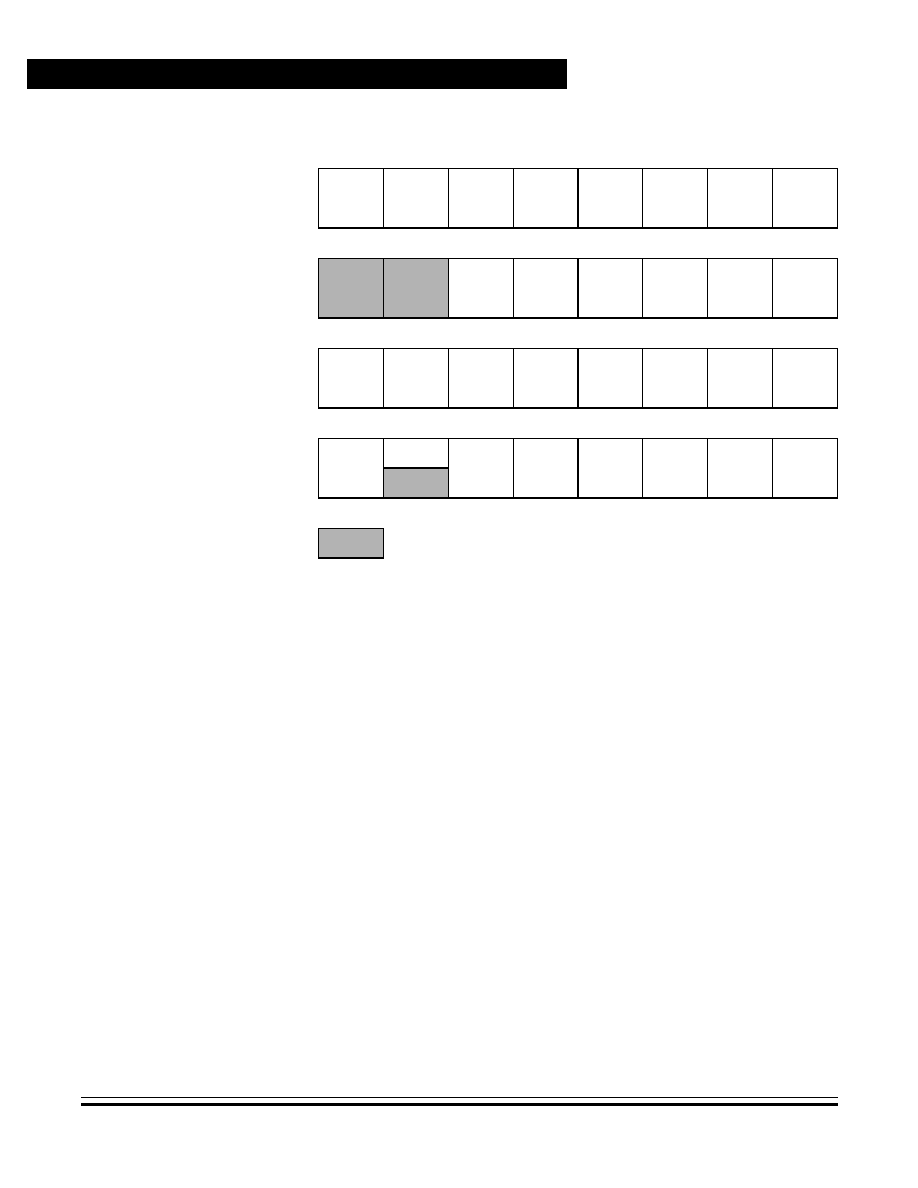
Input/Output (I/O) Ports
Advance Information
MC68HC908RK2
--
Rev. 4.0
174
Input/Output (I/O) Ports
MOTOROLA
Addr.
Register Name
Bit 7
6
5
4
3
2
1
Bit 0
$0000
Port A Data Register
(PTA)
See page 175.
Read:
PTA7
PTA6
PTA5
PTA4
PTA3
PTA2
PTA1
PTA0
Write:
Reset:
Unaffected by reset
$0001
Port B Data Register
(PTB)
See page 178.
Read:
PTB5
PTB4
PTB3
PTB2
PTB1
PTB0
Write:
Reset:
Unaffected by reset
$0004
Data Direction Register A
(DDRA)
See page 176.
Read:
DDRA7
DDRA6
DDRA5
DDRA4
DDRA3
DDRA2
DDRA1
DDRA0
Write:
Reset:
0
0
0
0
0
0
0
0
$0005
Data Direction Register B
(DDRB)
See page 179.
Read:
MCLKEN
0
DDRB5
DDRB4
DDRB3
DDRB2
DDRB1
DDRB0
Write:
Reset:
0
0
0
0
0
0
0
0
= Unimplemented
Figure 13-1. I/O Port Register Summary
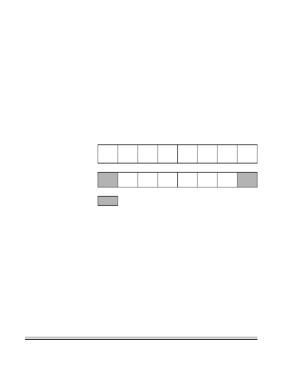
Input/Output (I/O) Ports
Port A
MC68HC908RK2
--
Rev. 4.0
Advance Information
MOTOROLA
Input/Output (I/O) Ports
175
13.3 Port A
Port A is an 8-bit special function port that shares six of its pins with the
keyboard interrupt module (KBD). PTA6≠PTA1 contain pullup resistors
enabled when the port pin is enabled as a keyboard interrupt. Port A pins
are also high-current port pins with 3-mA sink capabilities.
13.3.1 Port A Data Register
The port A data register (PTA) contains a data latch for each of the eight
port A pins.
PTA[7:0] -- Port A Data Bits
These read/write bits are software programmable. Data direction of
each port A pin is under the control of the corresponding bit in data
direction register A. Reset has no effect on port A data.
KBD[6:1] -- Keyboard Wakeup Pins
The keyboard interrupt enable bits, KBIE[6:1], in the keyboard
interrupt control register enable the port A pin as external interrupt
pins and related internal pullup resistor. See
Section 14.
Keyboard/External Interrupt Module (KBI)
.
NOTE:
The enabling of a keyboard interrupt pin will overide the corresponding
definition of the pin in the data direction register. However, the data
direction register bit must be a logic 0 for software to read the pin.
Address:
$0000
Bit 7
6
5
4
3
2
1
Bit 0
Read:
PTA7
PTA6
PTA5
PTA4
PTA3
PTA2
PTA1
PTA0
Write:
Reset:
Unaffected by reset
Alternate
Function:
KBD6
KBD5
KBD4
KBD3
KBD2
KBD1
= Unimplemented
Figure 13-2. Port A Data Register (PTA)

Input/Output (I/O) Ports
Advance Information
MC68HC908RK2
--
Rev. 4.0
176
Input/Output (I/O) Ports
MOTOROLA
13.3.2 Data Direction Register A
Data direction register A (DDRA) determines whether each port A pin is
an input or an output. Writing a logic 1 to a DDRA bit enables the output
buffer for the corresponding port A pin; a logic 0 disables the output
buffer.
DDRA[7:0] -- Data Direction Register A Bits
These read/write bits control port A data direction. Reset clears
DDRA[7:0], configuring all port A pins as inputs.
1 = Corresponding port A pin configured as output
0 = Corresponding port A pin configured as input
NOTE:
Avoid glitches on port A pins by writing to the port A data register before
changing data direction register A bits from 0 to 1.
Figure 13-4
shows the port A I/O logic.
When bit DDRAx is a logic 1, reading address $0000 reads the PTAx
data latch. When bit DDRAx is a logic 0, reading address $0000 reads
the voltage level on the pin. The data latch can always be written,
regardless of the state of its data direction bit.
Table 13-1
summarizes
the operation of the port A pins.
Address:
$0004
Bit 7
6
5
4
3
2
1
Bit 0
Read:
DDRA7
DDRA6
DDRA5
DDRA4
DDRA3
DDRA2
DDRA1
DDRA0
Write:
Reset:
0
0
0
0
0
0
0
0
Figure 13-3. Data Direction Register A (DDRA)
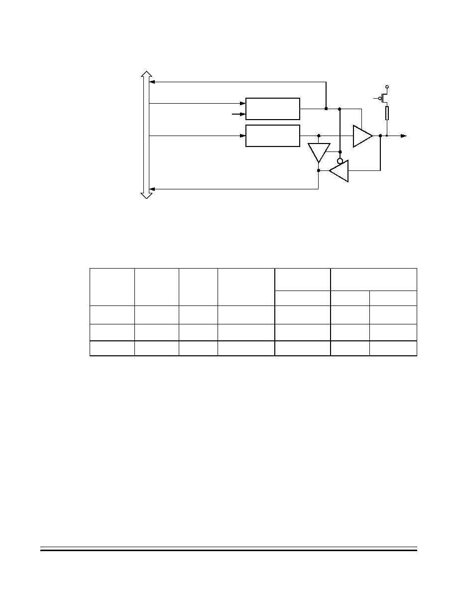
Input/Output (I/O) Ports
Port A
MC68HC908RK2
--
Rev. 4.0
Advance Information
MOTOROLA
Input/Output (I/O) Ports
177
Figure 13-4. Port A I/O Circuit
NOTE:
Setting a keyboard interrupt enable bit (KBIEx) forces the corresponding
keyboard interrupt pin to be an input, overriding the data direction
register. However, the data direction register bit must be a logic 0 for
software to read the pin.
READ DDRA ($0004)
WRITE DDRA ($0004)
RESET
WRITE PTA ($0000)
READ PTA ($0000)
DDRAx
PTAx
INT
E
RNA
L
DA
T
A
B
U
S
PTAx
V
DD
KBIE
X
INTERNAL
PULLUP
DEVICE
Table 13-1. Port A Pin Functions
KBIE
(2)
Bit
DDRA Bit
PTA Bit
I/O Pin Mode
Accesses
to DDRA
Accesses to PTA
Read/Write
Read
Write
1
X
X
(1)
Input, V
DD
(4)
DDRA[7:0]
Pin
PTA[7:0]
(3)
0
0
X
Input, Hi-Z
(5)
DDRA[7:0]
Pin
PTA[7:0]
(3)
0
1
X
Output
DDRA[7:0]
PTA[7:0]
PTA[7:0]
Notes:
1. X = Don't care
2. Keyboard interrupt enable bit (see
14.6.2 Keyboard Interrupt Enable Register
)
3. Writing affects data register, but does not affect input.
4. I/O pin pulled up to V
DD
by internal pullup device
5. Hi-Z = High impedance
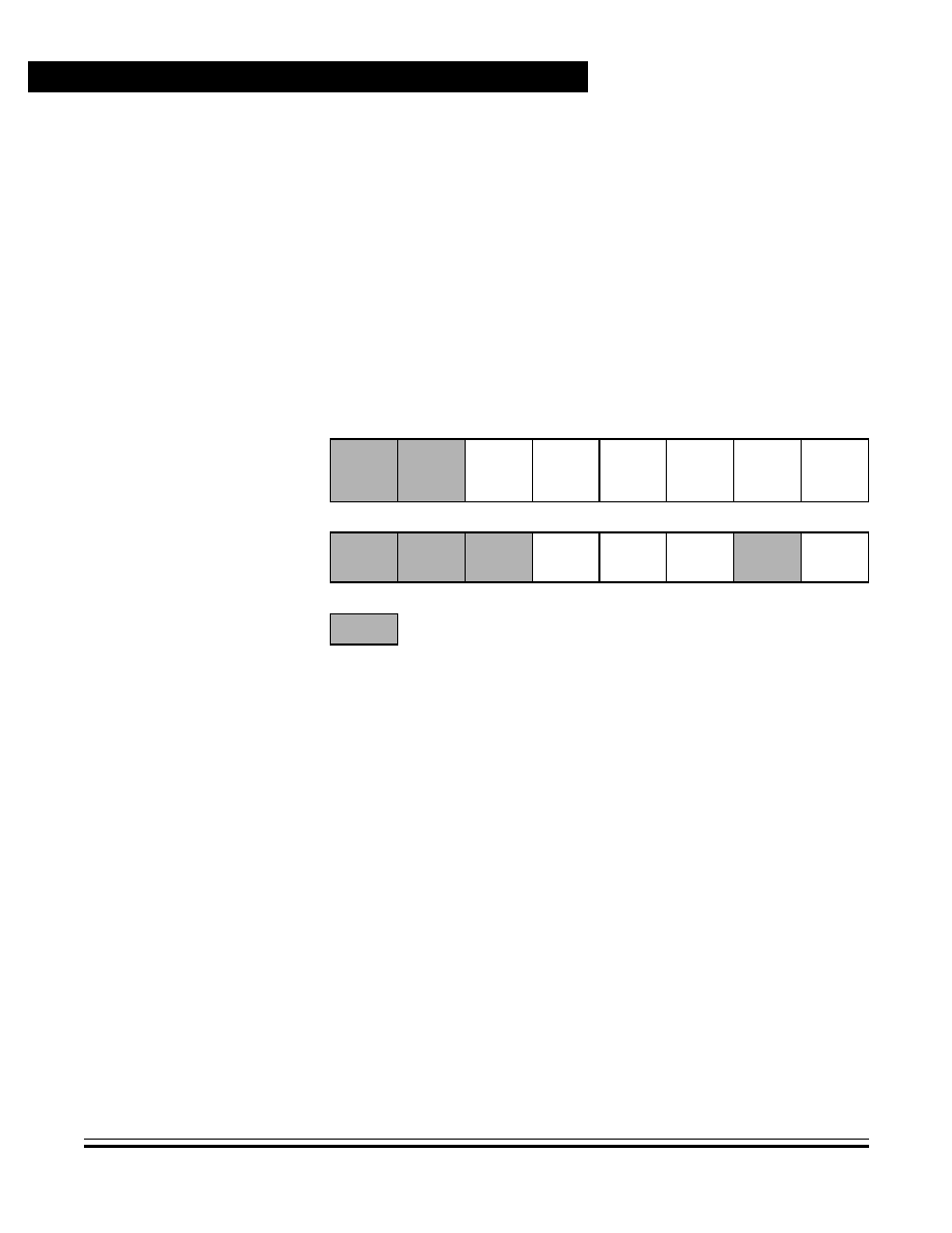
Input/Output (I/O) Ports
Advance Information
MC68HC908RK2
--
Rev. 4.0
178
Input/Output (I/O) Ports
MOTOROLA
13.4 Port B
Port B is a 6-bit special function port that shares three of its pins with the
timer (TIM) module and one with the buffered internal bus clock MCLK.
13.4.1 Port B Data Register
The port B data register (PTB) contains a data latch for each of the six
port B pins.
PTB[5:0] -- Port B Data Bits
These read/write bits are software-programmable. Data direction of
each port B pin is under the control of the corresponding bit in data
direction register B. Reset has no effect on port B data.
TCH1 -- Timer Channel I/O Bit
The PTB4/TCH1 pin is the TIM channel 1input capture/output
compare pin. The edge/level select bits, ELS1B:ELS1A, determine
whether the PTB4/TCH1 pin is a timer channel I/O or a general-
purpose I/O pin. See
Section 15. Timer Interface Module (TIM)
.
TCH0 -- Timer Channel I/O Bit
The PTB2/TCH0 pin is the TIM channel 0 input capture/output
compare pin. The edge/level select bits, ELS0B:ELS0A, determine
whether the PTB2/TCH0 pin is a timer channel I/O or a general-
purpose I/O pin. See
Section 15. Timer Interface Module (TIM)
.
Address:
$0001
Bit 7
6
5
4
3
2
1
Bit 0
Read:
PTB5
PTB4
PTB3
PTB2
PTB1
PTB0
Write:
Reset:
Unaffected by reset
Alternate
Functions:
TCH1
TCLK
TCH0
MCLK
= Unimplemented
Figure 13-5. Port B Data Register (PTB)

Input/Output (I/O) Ports
Port B
MC68HC908RK2
--
Rev. 4.0
Advance Information
MOTOROLA
Input/Output (I/O) Ports
179
TCLK -- Timer Clock
The PTB3/TCLK pin is the external clock input for TIM. The prescaler
select bits, PS[2:0], select PTB3/TCLK as the TIM clock input. (See
15.9.1 TIM Status and Control Register
.) When not selected as the
TIM clock, PTB3/TCLK is available for general-purpose I/O.
MCLK -- Bus Clock
The bus clock (MCLK) is driven out of pin PTB0/MCLK when enabled
by the MCLKEN bit in port B data direction register bit 7.
13.4.2 Data Direction Register B
Data direction register B (DDRB) determines whether each port B pin is
an input or an output. Writing a logic 1 to a DDRB bit enables the output
buffer for the corresponding port B pin; a logic 0 disables the output
buffer.
MCLKEN -- MCLK Enable Bit
This read/write bit enables MCLK to be an output signal on PTB0. If
MCLK is enabled, PTB0 is under the control of MCLKEN. Reset
clears this bit.
1 = MCLK output enabled
0 = MCLK output disabled
DDRB[5:0] -- Data Direction Register B Bits
These read/write bits control port B data direction. Reset clears
DDRB[5:0], configuring all port B pins as inputs.
1 = Corresponding port B pin configured as output
0 = Corresponding port B pin configured as input
Address:
$0005
Bit 7
6
5
4
3
2
1
Bit 0
Read:
MCLKEN
0
DDRB5
DDRB4
DDRB3
DDRB2
DDRB1
DDRB0
Write:
Reset:
0
0
0
0
0
0
0
0
= Unimplemented
Figure 13-6. Data Direction Register B (DDRB)
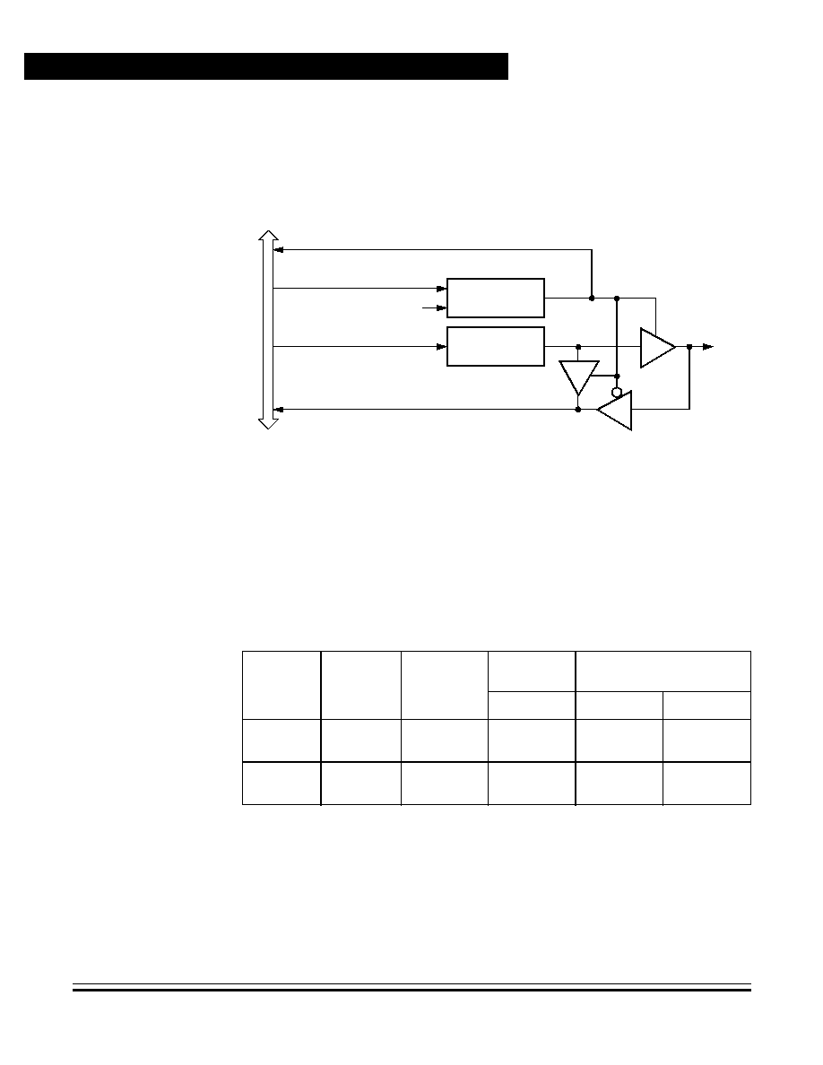
Input/Output (I/O) Ports
Advance Information
MC68HC908RK2
--
Rev. 4.0
180
Input/Output (I/O) Ports
MOTOROLA
NOTE:
Avoid glitches on port B pins by writing to the port B data register before
changing data direction register B bits from 0 to 1.
Figure 13-7
shows the port B I/O logic.
Figure 13-7. Port B I/O Circuit
When bit DDRBx is a logic 1, reading address $0001 reads the PTBx
data latch. When bit DDRBx is a logic 0, reading address $0001 reads
the voltage level on the pin. The data latch can always be written,
regardless of the state of its data direction bit.
Table 13-2
summarizes
the operation of the port B pins.
Table 13-2. Port B Pin Functions
DDRB
Bit
PTB
Bit
I/O Pin
Mode
Accesses
to DDRB
Accesses to PTB
Read/Write
Read
Write
0
X
Input, Hi-Z
DDRB[7]
DDRB[5:0]
Pin
PTB[5:0]
(1)
1
X
Output
DDRB[7]
DDRB[5:0]
PTB[5:0]
PTB[5:0]
X = Don't care
Hi-Z = High impedance
1. Writing affects data register, but does not affect input.
READ DDRB ($0005)
WRITE DDRB ($0005)
RESET
WRITE PTB ($0001)
READ PTB ($0001)
PTBx
DDRBx
PTBx
IN
TE
RNA
L
DA
T
A
B
U
S

MC68HC908RK2
--
Rev. 4.0
Advance Information
MOTOROLA
Keyboard/External Interrupt Module (KBI)
181
Advance Information -- MC68HC908RK2
Section 14. Keyboard/External Interrupt Module (KBI)
14.1 Contents
14.2
Introduction . . . . . . . . . . . . . . . . . . . . . . . . . . . . . . . . . . . . . . . 181
14.3
Features . . . . . . . . . . . . . . . . . . . . . . . . . . . . . . . . . . . . . . . . . 182
14.4
Functional Description . . . . . . . . . . . . . . . . . . . . . . . . . . . . . . 182
14.4.1
External Interrupt . . . . . . . . . . . . . . . . . . . . . . . . . . . . . . . .182
14.4.2
IRQ1 Pin. . . . . . . . . . . . . . . . . . . . . . . . . . . . . . . . . . . . . . . 186
14.4.3
KBI Module During Break Interrupts. . . . . . . . . . . . . . . . . . 187
14.4.4
Keyboard Interrupt Pins . . . . . . . . . . . . . . . . . . . . . . . . . . . 187
14.4.5
Keyboard Initialization . . . . . . . . . . . . . . . . . . . . . . . . . . . . 189
14.5
Low-Power Modes . . . . . . . . . . . . . . . . . . . . . . . . . . . . . . . . . 190
14.5.1
Wait Mode . . . . . . . . . . . . . . . . . . . . . . . . . . . . . . . . . . . . .190
14.5.2
Stop Mode . . . . . . . . . . . . . . . . . . . . . . . . . . . . . . . . . . . . .190
14.6
I/O Registers. . . . . . . . . . . . . . . . . . . . . . . . . . . . . . . . . . . . . . 191
14.6.1
IRQ and Keyboard Status and Control Register . . . . . . . . 191
14.6.2
Keyboard Interrupt Enable Register . . . . . . . . . . . . . . . . . . 193
14.2 Introduction
This section describes the maskable external interrupt (IRQ1) input and
six independently maskable keyboard wakeup interrupt pins.

Keyboard/External Interrupt Module (KBI)
Advance Information
MC68HC908RK2
--
Rev. 4.0
182
Keyboard/External Interrupt Module (KBI)
MOTOROLA
14.3 Features
Features of the KBI include:
∑
Dedicated external interrupt pin (IRQ1)
∑
Six keyboard interrupt pins with separate keyboard interrupt
enable bits and one keyboard interrupt mask
∑
Internal pullup resistor
∑
Hysteresis buffer
∑
Programmable edge-only or edge- and level-interrupt sensitivity
∑
Automatic interrupt acknowledge
14.4 Functional Description
This section provides a functional description of the keyboard/external
interrupt module (KBI).
14.4.1 External Interrupt
A logic 0 applied to the external interrupt pin (IRQ1) can latch a CPU
interrupt request.
Figure 14-1
shows the structure of the external (IRQ1)
interrupt of the KBI module.
A logic 0 applied to one or more of the keyboard interrupt pins can latch
a CPU interrupt request.
Figure 14-4
shows the structure of the
keyboard interrupts of the KBI module
See
Figure 14-2
for a summary of the interrupt and keyboard
input/output (I/O) registers.
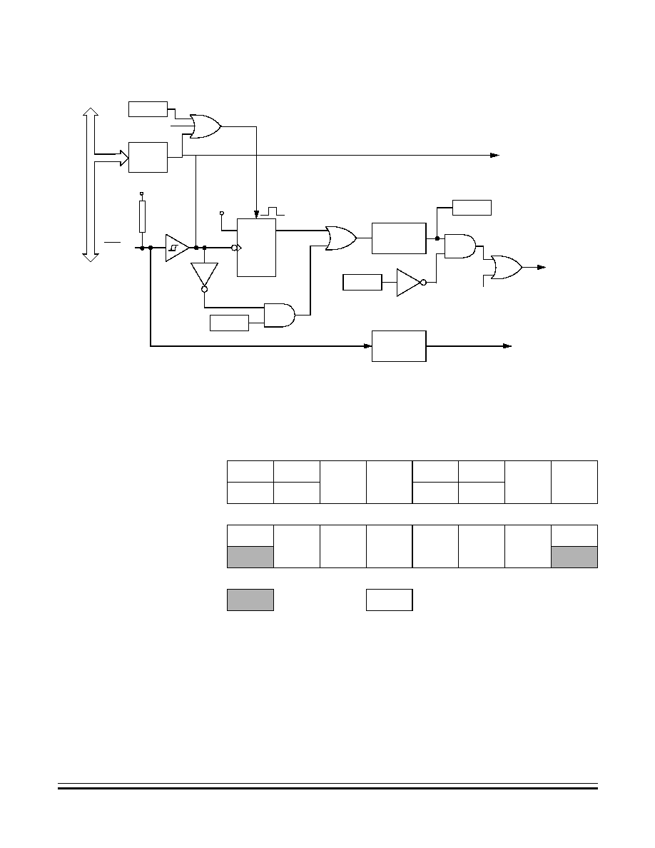
Keyboard/External Interrupt Module (KBI)
Functional Description
MC68HC908RK2
--
Rev. 4.0
Advance Information
MOTOROLA
Keyboard/External Interrupt Module (KBI)
183
Figure 14-1. IRQ Block Diagram
ACKI
IMASKI
D
Q
CK
CLR
IRQ1
HIGH
INTERRUPT
TO MODE
SELECT
LOGIC
IRQ1
LATCH
REQUEST
IRQ1
V
DD
MODEI
VOLTAGE
DETECT
SYNCHRO-
NIZER
IRQ1F
TO CPU FOR
BIL/BIH
INSTRUCTIONS
VECTOR
FETCH
DECODER
I
N
T
E
R
N
A
L AD
D
R
ES
S
B
U
S
V
DD
KEYBOARD
INTERRUPT
REQUEST
IRQ1/KEYBOARD
INTERRUPT
REQUEST
INTERNAL
PULLUP
DEVICE
RESET
Addr.
Register Name
Bit 7
6
5
4
3
2
1
Bit 0
$001A
IRQ and Keyboard Status
and Control Register
(INTKBSCR)
See page 191.
Read:
IRQ1F
0
IMASKI
MODEI
KEYF
0
IMASKK
MODEK
Write:
R
ACKI
R
ACKK
Reset:
0
0
0
0
0
0
0
0
$001B
Keyboard Interrupt Enable
Register
(INTKBIER)
See page 193.
Read:
0
KBIE6
KBIE5
KBIE4
KBIE3
KBIE2
KBIE1
0
Write:
Reset:
0
0
0
0
0
0
0
0
= Unimplemented
R
= Reserved
Figure 14-2. IRQ and Keyboard I/O Register Summary

Keyboard/External Interrupt Module (KBI)
Advance Information
MC68HC908RK2
--
Rev. 4.0
184
Keyboard/External Interrupt Module (KBI)
MOTOROLA
Interrupt signals on the IRQ1 pin are latched into the IRQ1 latch.
Keyboard interrupts are latched in the keyboard interrupt latch. An
interrupt latch remains set until one of these actions occurs:
∑
Vector fetch -- A vector fetch automatically generates an interrupt
acknowledge signal that clears IRQ1 latch and keyboard interrupt
latch.
∑
Software clear -- Software can clear an interrupt latch by writing
to the appropriate acknowledge bit in the interrupt status and
control register (INTKBSCR). Writing a logic 1 to the ACKI bit
clears the IRQ1 latch. Writing a logic 1 to the ACKK bit clears the
keyboard interrupt latch.
∑
Reset -- A reset automatically clears both interrupt latches.
The IRQ1 pin and keyboard interrupt pins are falling-edge triggered and
are software-configurable to be both falling-edge and low-level triggered.
The MODEI and MODEK bits in the INTKBSCR controls the triggering
sensitivity of the IRQ1 pin and keyboard interrupt pins.
When an interrupt pin is edge-triggered only, the interrupt latch remains
set until a vector fetch, software clear, or reset occurs.
When an interrupt pin is both falling-edge and low-level-triggered, the
interrupt latch remains set until both of these occur:
∑
Vector fetch or software clear
∑
Return of the interrupt pin to logic 1
The vector fetch or software clear may occur before or after the interrupt
pin returns to logic 1. As long as the pin is low, the interrupt request
remains pending. A reset will clear the latch, the MODEI and MODEK
control bits, thereby clearing the interrupt even if the pin stays low.
When set, the IMASKI and IMASKK bits in the INTKBSCR masks all
external interrupt requests. A latched interrupt request is not presented
to the interrupt priority logic unless the corresponding IMASK<x> bit is
clear.
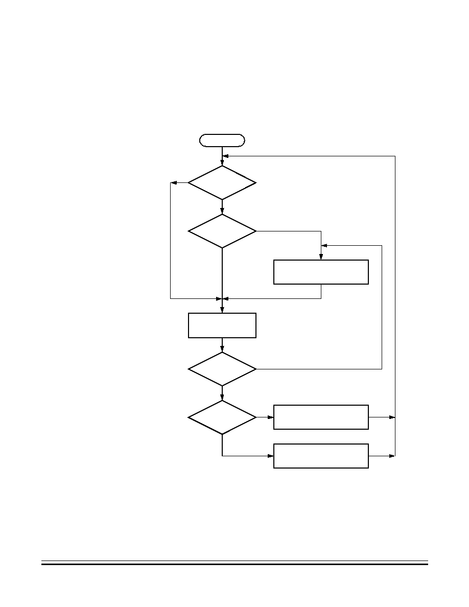
Keyboard/External Interrupt Module (KBI)
Functional Description
MC68HC908RK2
--
Rev. 4.0
Advance Information
MOTOROLA
Keyboard/External Interrupt Module (KBI)
185
NOTE:
The interrupt mask (I) in the condition code register (CCR) masks all
interrupt requests, including external interrupt requests.
(See
Figure 14-3
.)
Figure 14-3. IRQ Interrupt Flowchart
FROM RESET
I BIT SET?
FETCH NEXT
YES
NO
INTERRUPT?
INSTRUCTION
SWI
INSTRUCTION?
RTI
INSTRUCTION?
NO
STACK CPU REGISTERS
NO
SET I BIT
LOAD PC WITH INTERRUPT VECTOR
NO
YES
UNSTACK CPU REGISTERS
EXECUTE INSTRUCTION
YES
YES

Keyboard/External Interrupt Module (KBI)
Advance Information
MC68HC908RK2
--
Rev. 4.0
186
Keyboard/External Interrupt Module (KBI)
MOTOROLA
14.4.2 IRQ1 Pin
A logic 0 on the IRQ1 pin can latch an interrupt request into the IRQ1
latch. A vector fetch, software clear, or reset clears the IRQ1 latch. If the
MODEI bit is set, the IRQ1 pin is both falling-edge sensitive and low-level
sensitive. With MODEI set, both of these actions must occur to clear the
IRQ1 latch:
∑
Vector fetch or software clear -- A vector fetch generates an
interrupt acknowledge signal to clear the latch. Software may
generate the interrupt acknowledge signal by writing a logic 1 to
the ACKI bit in the IRQ and keyboard status and control register
(INTKBSCR). The ACKI bit is useful in applications that poll the
IRQ1 pin and require software to clear the IRQ1 latch. Writing to
the ACKI bit can also prevent spurious interrupts due to noise.
Setting ACKI does not affect subsequent transitions on the IRQ1
pin. A falling edge on IRQ1 that occurs after writing to the ACKI bit
latches another interrupt request. If the IRQ1 mask bit, IMASKI, is
clear, the CPU loads the program counter with the vector address
at locations $FFFA and $FFFB.
∑
Return of the IRQ1 pin to logic 1 -- As long as the IRQ1 pin is at
logic 0, the IRQ1 latch remains set.
The vector fetch or software clear and the return of the IRQ1 pin to
logic 1 can occur in any order. The interrupt request remains pending as
long as the IRQ1 pin is at logic 0. A reset will clear the latch and the
MODEI control bit, thereby clearing the interrupt even if the pin stays low.
If the MODEI bit is clear, the IRQ1 pin is falling-edge sensitive only. With
MODEI clear, a vector fetch or software clear immediately clears the
IRQ1 latch.The IRQ1F bit in the INTKBSCR register can be used to
check for pending interrupts. The IRQ1F bit is not affected by the IMASKI
bit, which makes it useful in applications where polling is preferred.
Use the BIH or BIL instruction to read the logic level on the IRQ1 pin.
NOTE:
When using the level-sensitive interrupt trigger, avoid false interrupts by
masking interrupt requests in the interrupt routine.

Keyboard/External Interrupt Module (KBI)
Functional Description
MC68HC908RK2
--
Rev. 4.0
Advance Information
MOTOROLA
Keyboard/External Interrupt Module (KBI)
187
14.4.3 KBI Module During Break Interrupts
The system integration module (SIM) controls whether the IRQ1 or
keyboard interrupt latchs can be cleared during the break state. The
BCFE bit in the break flag control register (BFCR) enables software to
clear the latches during the break state. (See
6.8.3 SIM Break Flag
Control Register
.)
To allow software to clear the IRQ1 or keyboard latchs during a break
interrupt, write a logic 1 to the BCFE bit. If a latch is cleared during the
break state, it remains cleared when the MCU exits the break state.
To protect the latch during the break state, write a logic 0 to the BCFE
bit. With BCFE at logic 0 (its default state), writing to the ACKI or ACKK
bits in the IRQ and keyboard status and control register during the break
state has no effect on the IRQ1 or keyboard latchs.
14.4.4 Keyboard Interrupt Pins
Writing to the KBIE6≠KBIE1 bits in the keyboard interrupt enable register
independently enables or disables each port A pin as a keyboard
interrupt pin. Enabling a keyboard interrupt pin also enables its internal
pullup device. A logic 0 applied to an enabled keyboard interrupt pin
latches an IRQ1/keyboard interrupt request.
An IRQ1/keyboard interrupt is latched when one or more keyboard pins
goes low after all were high. The MODEK bit in the keyboard status and
control register controls the triggering mode of the keyboard interrupt.
∑
If the keyboard interrupt is edge-sensitive only, a falling edge on a
keyboard pin does not latch an interrupt request if another
keyboard pin is already low. To prevent losing an interrupt request
on one pin because another pin is still low, software can disable
the latter pin while it is low.
∑
If the keyboard interrupt is falling edge- and low level-sensitive, an
interrupt request is present as long as any keyboard pin is low.
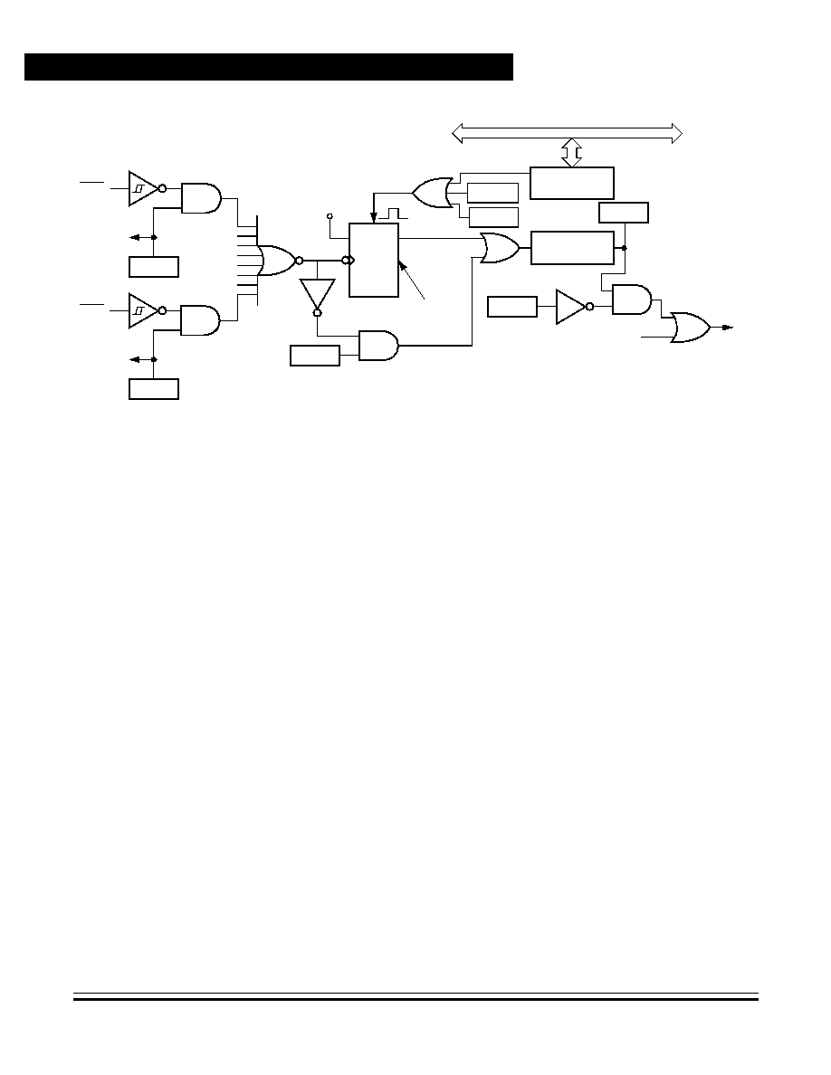
Keyboard/External Interrupt Module (KBI)
Advance Information
MC68HC908RK2
--
Rev. 4.0
188
Keyboard/External Interrupt Module (KBI)
MOTOROLA
Figure 14-4. Keyboard Interrupt Block Diagram
If the MODEK bit is set, the keyboard interrupt pins are both falling edge-
and low level-sensitive, and both of these actions must occur to clear a
keyboard interrupt request:
∑
Vector fetch or software clear -- A vector fetch generates an
interrupt acknowledge signal to clear the interrupt request.
Software may generate the interrupt acknowledge signal by
writing a logic 1 to the ACKK bit in the keyboard status and control
register (INTKBSCR). The ACKK bit is useful in applications that
poll the keyboard interrupt pins and require software to clear the
keyboard interrupt request. Writing to the ACKK bit prior to leaving
an interrupt service routine also can prevent spurious interrupts
due to noise. Setting ACKK does not affect subsequent transitions
on the keyboard interrupt pins. A falling edge that occurs after
writing to the ACKK bit latches another interrupt request. If the
keyboard interrupt mask bit, IMASKK, is clear, the CPU loads the
program counter with the vector address at locations $FFFA and
$FFFB.
∑
Return of all enabled keyboard interrupt pins to logic 1. As long as
any enabled keyboard interrupt pin is at logic 0, the keyboard
interrupt remains set.
KB1IE
KB6IE
.
.
.
KEYBOARD
INTERRUPT
D
Q
CK
CLR
V
DD
MODEK
IMASKK
KEYBOARD
INTERRUPT LATCH
REQUEST
VECTOR FETCH
DECODER
ACKK
INTERNAL BUS
RESET
TO PULLUP
KBD6
KBD1
TO PULLUP
SYNCHRONIZER
KEYF
ENABLE
ENABLE
IRQ1
INTERRUPT
REQUEST
IRQ1/KEYBOARD
INTERRUPT
REQUEST

Keyboard/External Interrupt Module (KBI)
Functional Description
MC68HC908RK2
--
Rev. 4.0
Advance Information
MOTOROLA
Keyboard/External Interrupt Module (KBI)
189
The vector fetch or software clear and the return of all enabled keyboard
interrupt pins to logic 1 may occur in any order.
If the MODEK bit is clear, the keyboard interrupt pin is falling edge-
sensitive only. With MODEK clear, a vector fetch or software clear
immediately clears the keyboard interrupt request.
Reset clears the keyboard interrupt request and the MODEK bit, clearing
the interrupt request even if a keyboard interrupt pin stays at logic 0.
The keyboard flag bit (KEYF) in the IRQ and keyboard status and control
register can be used to see if a pending interrupt exists. The KEYF bit is
not affected by the keyboard interrupt mask bit (IMASKK) which makes
it useful in applications where polling is preferred.
To determine the logic level on a keyboard interrupt pin, use the data
direction register to configure the pin as an input and read the data
register.
NOTE:
Setting a keyboard interrupt enable bit (KBIE<x>) forces the
corresponding keyboard interrupt pin to be an input, overriding the data
direction register. However, the data direction register bit must be a logic
0 for software to read the pin.
14.4.5 Keyboard Initialization
When a keyboard interrupt pin is enabled, it takes time for the internal
pullup to reach a logic 1. Therefore, a false interrupt can occur as soon
as the pin is enabled.
To prevent a false interrupt on keyboard initialization:
1. Mask keyboard interrupts by setting the IMASKK bit in the
keyboard status and control register.
2. Enable the KBI pins by setting the appropriate KBIEx bits in the
keyboard interrupt enable register.
3. Write to the ACKK bit in the keyboard status and control register
to clear any false interrupts.
4. Clear the IMASKK bit.

Keyboard/External Interrupt Module (KBI)
Advance Information
MC68HC908RK2
--
Rev. 4.0
190
Keyboard/External Interrupt Module (KBI)
MOTOROLA
An interrupt signal on an edge-triggered pin can be acknowledged
immediately after enabling the pin. An interrupt signal on an edge- and
level-triggered interrupt pin must be acknowledged after a delay that
depends on the external load.
Another way to avoid a false interrupt:
1. Configure the keyboard pins as outputs by setting the appropriate
DDRA bits in data direction register A.
2. Write logic 1s to the appropriate port A data register bits.
3. Enable the KBI pins by setting the appropriate KBIEx bits in the
keyboard interrupt enable register.
14.5 Low-Power Modes
The WAIT and STOP instructions put the MCU in low power-
consumption standby modes.
14.5.1 Wait Mode
The IRQ1/keyboard interrupts remain active in wait mode. Clearing the
IMASKI or IMASKK bits in the IRQ and keyboard status and control
register enables keyboard interrupt requests to bring the MCU out of wait
mode.
14.5.2 Stop Mode
The IRQ1/keyboard interrupt remains active in stop mode. Clearing the
IMASKI or IMASKK bit in the IRQ and keyboard status and control
register enables keyboard interrupt requests to bring the MCU out of
stop mode.

Keyboard/External Interrupt Module (KBI)
I/O Registers
MC68HC908RK2
--
Rev. 4.0
Advance Information
MOTOROLA
Keyboard/External Interrupt Module (KBI)
191
14.6 I/O Registers
These registers control and monitor operation of the keyboard/external
interrupt module:
∑
IRQ and keyboard status and control register (INTKBSCR)
∑
Keyboard interrupt enable register (KBIER)
14.6.1 IRQ and Keyboard Status and Control Register
The IRQ and keyboard status and control register (INTKBSCR) controls
and monitors operation of the keyboard/external interrupt module. The
INTKBSCR has these functions:
∑
Flags the keyboard interrupt requests
∑
Acknowledges the keyboard interrupt requests
∑
Masks the keyboard interrupt requests
∑
Shows the state of the IRQ1 interrupt flag
∑
Clears the IRQ1 interrupt latch
∑
Masks the IRQ1 interrupt request
∑
Controls the triggering sensitivity of the keyboard and IRQ1
interrupt pins
IRQ1F -- IRQ1 Flag Bit
This read-only status bit is high when the IRQ1 interrupt is pending.
1 = IRQ1 interrupt pending
0 = IRQ1 interrupt not pending
Address: $001A
Bit 7
6
5
4
3
2
1
Bit 0
Read:
IRQ1F
0
IMASKI
MODEI
KEYF
0
IMASKK
MODEK
Write:
R
ACKI
R
ACKK
Reset:
0
0
0
0
0
0
0
0
R
= Reserved
Figure 14-5. IRQ and Keyboard Status and Control Register
(INTKBSCR)

Keyboard/External Interrupt Module (KBI)
Advance Information
MC68HC908RK2
--
Rev. 4.0
192
Keyboard/External Interrupt Module (KBI)
MOTOROLA
ACKI -- IRQ1 Interrupt Request Acknowledge Bit
Writing a logic 1 to this write-only bit clears the IRQ1 latch. ACKI
always reads as logic 0. Reset clears ACKI.
IMASKI -- IRQ1 Interrupt Mask Bit
Writing a logic 1 to this read/write bit disables IRQ1 interrupt requests.
Reset clears IMASKI.
1 = IRQ1 interrupt requests disabled
0 = IRQ1 interrupt requests enabled
MODEI -- IRQ1 Triggering Sensitivity Bit
This read/write bit controls the triggering sensitivity of the IRQ1 pin.
Reset clears MODEI.
1 = IRQ1 interrupt requests on falling edges and low levels
0 = interrupt requests on falling edges only
KEYF -- Keyboard Flag Bit
This read-only bit is set when a keyboard interrupt is pending. Reset
clears the KEYF bit.
1 = Keyboard interrupt pending
0 = No keyboard interrupt pending
ACKK -- Keyboard Acknowledge Bit
Writing a logic 1 to this write-only bit clears the keyboard interrupt
request. ACKK always reads as logic 0. Reset clears ACKK.
IMASKK -- Keyboard Interrupt Mask Bit
Writing a logic 1 to this read/write bit prevents the output of the
keyboard interrupt mask from generating interrupt requests. Reset
clears the IMASKK bit.
1 = Keyboard interrupt requests masked
0 = Keyboard interrupt requests not masked
MODEK -- Keyboard Triggering Sensitivity Bit
This read/write bit controls the triggering sensitivity of the keyboard
interrupt pins. Reset clears MODEK.
1 = Keyboard interrupt requests on falling edges and low levels
0 = Keyboard interrupt requests on falling edges only
Keyboard/External Interrupt Module (KBI)
I/O Registers
MC68HC908RK2
--
Rev. 4.0
Advance Information
MOTOROLA
Keyboard/External Interrupt Module (KBI)
193
14.6.2 Keyboard Interrupt Enable Register
The keyboard interrupt enable register (INTKBIER) enables or disables
each port A pin to operate as a keyboard interrupt pin.
KBIE6≠KBIE1 -- Keyboard Interrupt Enable Bits
Each of these read/write bits enables the corresponding keyboard
interrupt pin to latch interrupt requests. These bits also enable the
corresponding internal pullup resistor which is enabled only when the
bit is set. Reset clears the keyboard interrupt enable register.
1 = PAx pin enabled as keyboard interrupt pin and corresponding
internal pullup resistor enabled
0 = PAx pin not enabled as keyboard interrupt pin and
corresponding internal pullup resistor disabled
NOTE:
Setting a keyboard interrupt enable bit (KBIEx) forces the corresponding
keyboard interrupt pin to be an input, overriding the data direction
register. However, the data direction register bit must be a logic 0 for
software to read the pin.
Address: $001B
Bit 7
6
5
4
3
2
1
Bit 0
Read:
0
KBIE6
KBIE5
KBIE4
KBIE3
KBIE2
KBIE1
0
Write:
Reset:
0
0
0
0
0
0
0
0
= Unimplemented
Figure 14-6. Keyboard Interrupt Enable Register (INTKBIER)

Keyboard/External Interrupt Module (KBI)
Advance Information
MC68HC908RK2
--
Rev. 4.0
194
Keyboard/External Interrupt Module (KBI)
MOTOROLA

MC68HC908RK2
--
Rev. 4.0
Advance Information
MOTOROLA
Timer Interface Module (TIM)
195
Advance Information -- MC68HC908RK2
Section 15. Timer Interface Module (TIM)
15.1 Contents
15.2
Introduction . . . . . . . . . . . . . . . . . . . . . . . . . . . . . . . . . . . . . . . 196
15.3
Features . . . . . . . . . . . . . . . . . . . . . . . . . . . . . . . . . . . . . . . . . 196
15.4
Pin Name Conventions . . . . . . . . . . . . . . . . . . . . . . . . . . . . . . 196
15.5
Functional Description . . . . . . . . . . . . . . . . . . . . . . . . . . . . . . 197
15.5.1
TIM Counter Prescaler . . . . . . . . . . . . . . . . . . . . . . . . . . . .199
15.5.2
Input Capture . . . . . . . . . . . . . . . . . . . . . . . . . . . . . . . . . . . 199
15.5.3
Output Compare . . . . . . . . . . . . . . . . . . . . . . . . . . . . . . . . .199
15.5.4
Unbuffered Output Compare . . . . . . . . . . . . . . . . . . . . . . .200
15.5.5
Buffered Output Compare . . . . . . . . . . . . . . . . . . . . . . . . . 201
15.5.6
Pulse-Width Modulation (PWM) . . . . . . . . . . . . . . . . . . . . . 201
15.5.7
Unbuffered PWM Signal Generation . . . . . . . . . . . . . . . . . 202
15.5.8
Buffered PWM Signal Generation . . . . . . . . . . . . . . . . . . . 203
15.5.9
PWM Initialization. . . . . . . . . . . . . . . . . . . . . . . . . . . . . . . . 204
15.6
Interrupts. . . . . . . . . . . . . . . . . . . . . . . . . . . . . . . . . . . . . . . . . 205
15.6.1
Low-Power Modes . . . . . . . . . . . . . . . . . . . . . . . . . . . . . . . 205
15.6.2
Wait Mode . . . . . . . . . . . . . . . . . . . . . . . . . . . . . . . . . . . . .206
15.6.3
Stop Mode . . . . . . . . . . . . . . . . . . . . . . . . . . . . . . . . . . . . .206
15.7
TIM During Break Interrupts . . . . . . . . . . . . . . . . . . . . . . . . . . 206
15.8
I/O Signals . . . . . . . . . . . . . . . . . . . . . . . . . . . . . . . . . . . . . . . 207
15.8.1
TIM Clock Pin (TCLK) . . . . . . . . . . . . . . . . . . . . . . . . . . . . 207
15.8.2
TIM Channel I/O Pins (TCH0 and TCH1) . . . . . . . . . . . . . .207
15.9
I/O Registers. . . . . . . . . . . . . . . . . . . . . . . . . . . . . . . . . . . . . . 208
15.9.1
TIM Status and Control Register . . . . . . . . . . . . . . . . . . . . 208
15.9.2
TIM Counter Registers . . . . . . . . . . . . . . . . . . . . . . . . . . . .210
15.9.3
TIM Counter Modulo Registers . . . . . . . . . . . . . . . . . . . . . 211
15.9.4
TIM Channel Status and Control Registers . . . . . . . . . . . . 211
15.9.5
TIM Channel Registers. . . . . . . . . . . . . . . . . . . . . . . . . . . .215

Timer Interface Module (TIM)
Advance Information
MC68HC908RK2
--
Rev. 4.0
196
Timer Interface Module (TIM)
MOTOROLA
15.2 Introduction
This section describes the timer interface module (TIM). The TIM is a
2-channel timer that provides a timing reference with input capture,
output compare, and pulse-width-modulation (PWM) functions.
Figure 15-1
is a block diagram of the TIM.
15.3 Features
Features of the TIM include:
∑
Two input capture/output compare channels:
≠
Rising-edge, falling-edge, or any-edge input capture trigger
≠
Set, clear, or toggle output compare action
∑
Buffered and unbuffered PWM signal generation
∑
Programmable TIM clock input:
≠
7-frequency internal bus clock prescaler selection
≠
External TIM clock input (bus frequency
˜
2 maximum)
∑
Free-running or modulo up-count operation
∑
Toggle any channel pin on overflow
∑
TIM counter stop and reset bits
15.4 Pin Name Conventions
The TIM module shares pins with three port B input/output (I/O) port
pins. The full names of the TIM I/O pins and generic pin names are listed
in
Table 15-1
.
Table 15-1. Pin Name Conventions
TIM Generic
Pin Names:
TCH0
TCH1
TCLK
Full TIM
Pin Names:
PTB2/TCH0
PTB4/TCH1
PTB3/TCLK
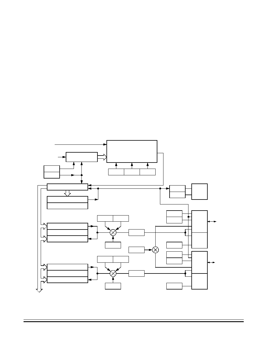
Timer Interface Module (TIM)
Functional Description
MC68HC908RK2
--
Rev. 4.0
Advance Information
MOTOROLA
Timer Interface Module (TIM)
197
15.5 Functional Description
Figure 15-1
shows the structure of the TIM. The central component of
the TIM is the 16-bit TIM counter that can operate as a free-running
counter or a modulo up-counter. The TIM counter provides the timing
reference for the input capture and output compare functions. The TIM
counter modulo registers, TMODH and TMODL, control the modulo
value of the TIM counter. Software can read the TIM counter value at any
time without affecting the counting sequence.
The two TIM channels are programmable independently as input
capture or output compare channels.
Refer to
Figure 15-2
for a summary of the TIM I/O registers.
Figure 15-1. TIM Block Diagram
PRESCALER
PRESCALER SELECT
16-BIT COMPARATOR
PS2
PS1
PS0
16-BIT COMPARATOR
16-BIT LATCH
TCH0H:TCH0L
MS0A
ELS0B
ELS0A
PORT
TOF
TOIE
INTER-
16-BIT COMPARATOR
16-BIT LATCH
TCH1H:TCH1L
CHANNEL 0
CHANNEL 1
TMODH:TMODL
TRST
TSTOP
TOV0
CH0IE
CH0F
ELS1B
ELS1A
TOV1
CH1IE
CH1MAX
CH1F
CH0MAX
MS0B
16-BIT COUNTER
INT
E
RNA
L
B
U
S
BUS CLOCK
MS1A
LOGIC
RUPT
LOGIC
INTER-
RUPT
LOGIC
PORT
LOGIC
INTER-
RUPT
LOGIC
PTB3/TCLK
PTB2/TCH0
PTB4/TCH1
INTERNAL
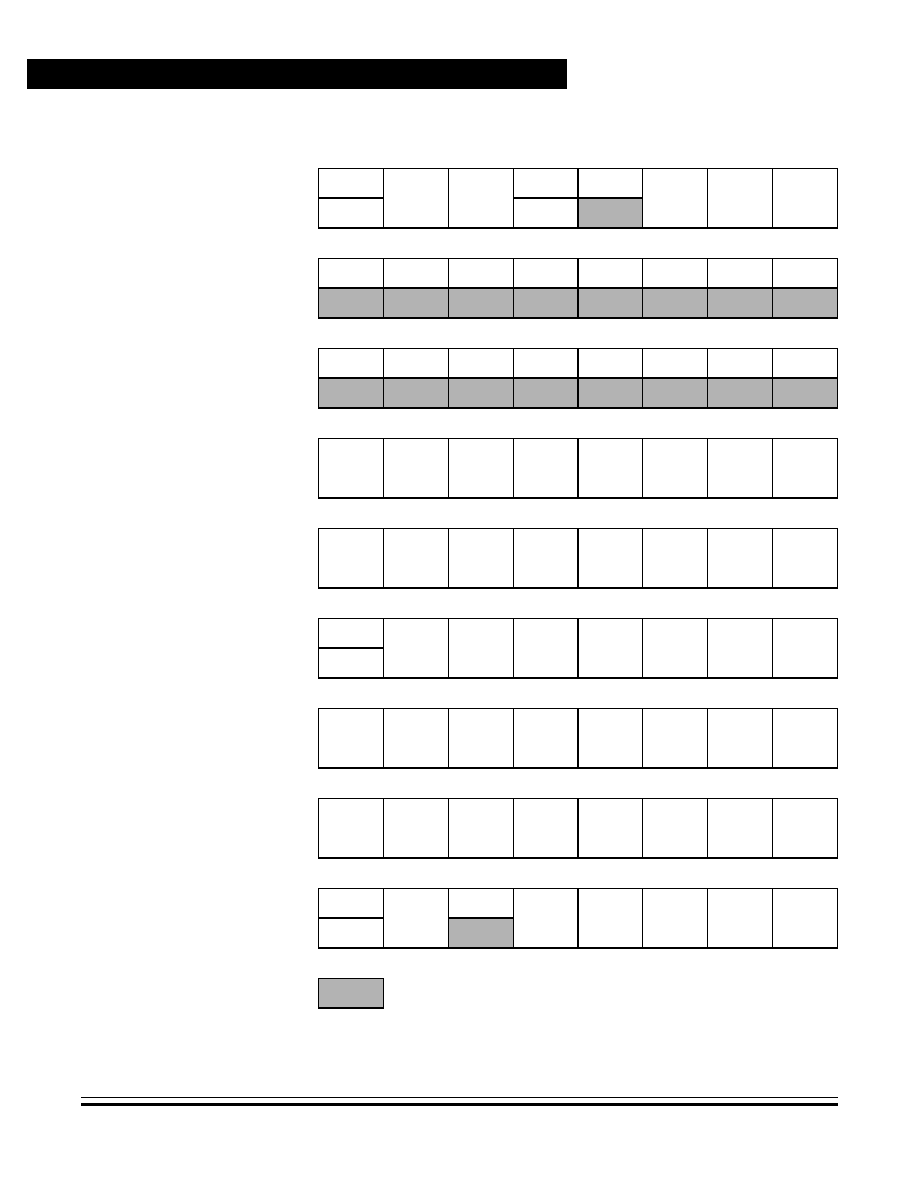
Timer Interface Module (TIM)
Advance Information
MC68HC908RK2
--
Rev. 4.0
198
Timer Interface Module (TIM)
MOTOROLA
Addr.
Register Name
Bit 7
6
5
4
3
2
1
Bit 0
$0020
Timer Status and Control
Register (TSC)
See page 208.
Read:
TOF
TOIE
TSTOP
0
0
PS2
PS1
PS0
Write:
0
TRST
Reset:
0
0
1
0
0
0
0
0
$0021
Timer Counter Register
High (TCNTH)
See page 210.
Read:
Bit 15
14
13
12
11
10
9
Bit 8
Write:
Reset:
0
0
0
0
0
0
0
0
$0022
Timer Counter Register
Low (TCNTL)
See page 210.
Read:
Bit 7
6
5
4
3
2
1
Bit 0
Write:
Reset:
0
0
0
0
0
0
0
0
$0023
Timer Counter Modulo
Register High (TMODH)
See page 211.
Read:
Bit 15
14
13
12
11
10
9
Bit 8
Write:
Reset:
1
1
1
1
1
1
1
1
$0024
Timer Counter Modulo
Register Low (TMODL)
See page 211.
Read:
Bit 7
6
5
4
3
2
1
Bit 0
Write:
Reset:
1
1
1
1
1
1
1
1
$0025
Timer Channel 0 Status
and Control Register
(TSC0)
See page 212.
Read:
CH0F
CH0IE
MS0B
MS0A
ELS0B
ELS0A
TOV0
CH0MAX
Write:
0
Reset:
0
0
0
0
0
0
0
0
$0026
Timer Channel 0 Register
High (TCH0H)
See page 216.
Read:
Bit 15
14
13
12
11
10
9
Bit 8
Write:
Reset:
Indeterminate after reset
$0027
Timer Channel 0 Register
Low (TCH0L)
See page 216.
Read:
Bit 7
6
5
4
3
2
1
Bit 0
Write:
Reset:
Indeterminate after reset
$0028
Timer Channel 1 Status
and Control Register
(TSC1)
See page 212.
Read:
CH1F
CH1IE
0
MS1A
ELS1B
ELS1A
TOV1
CH1MAX
Write:
0
Reset:
0
0
0
0
0
0
0
0
= Unimplemented
Figure 15-2. TIM I/O Register Summary
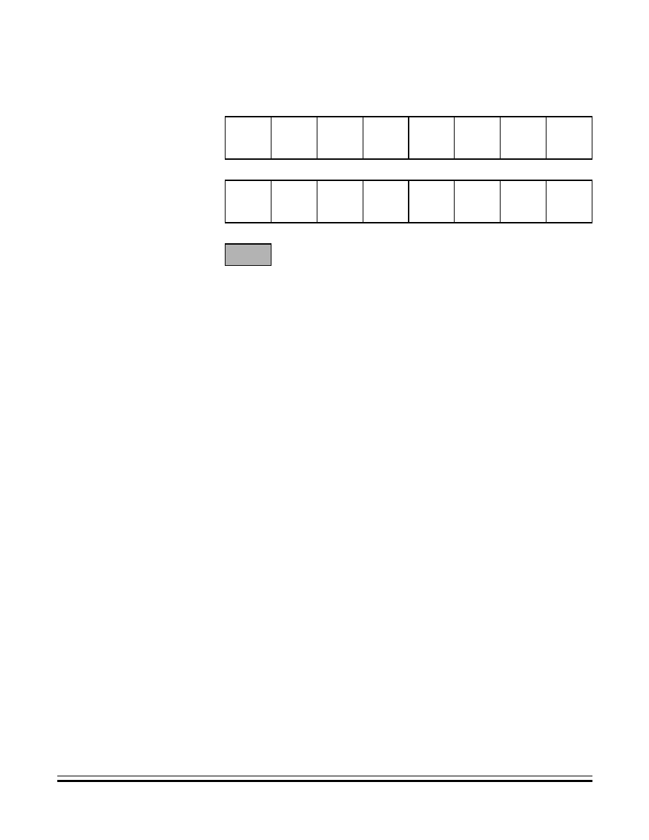
Timer Interface Module (TIM)
Functional Description
MC68HC908RK2
--
Rev. 4.0
Advance Information
MOTOROLA
Timer Interface Module (TIM)
199
15.5.1 TIM Counter Prescaler
The TIM clock source can be one of the seven prescaler outputs or the
TIM clock pin, TCLK. The prescaler generates seven clock rates from
the internal bus clock. The prescaler select bits, PS[2:0], in the TIM
status and control register select the TIM clock source.
15.5.2 Input Capture
With the input capture function, the TIM can capture the time at which an
external event occurs. When an active edge occurs on the pin of an input
capture channel, the TIM latches the contents of the TIM counter into the
TIM channel registers, TCHxH and TCHxL. The polarity of the active
edge is programmable. Input captures can generate TIM CPU interrupt
requests.
15.5.3 Output Compare
With the output compare function, the TIM can generate a periodic pulse
with a programmable polarity, duration, and frequency. When the
counter reaches the value in the registers of an output compare channel,
the TIM can set, clear, or toggle the channel pin. Output compares can
generate TIM CPU interrupt requests.
$0029
Timer Channel 1 Register
High (TCH1H))
See page 216.
Read:
Bit 15
14
13
12
11
10
9
Bit 8
Write:
Reset:
Indeterminate after reset
$002A
Timer Channel 1 Register
Low (TCH1L))
See page 216.
Read:
Bit 7
6
5
4
3
2
1
Bit 0
Write:
Reset:
Indeterminate after reset
Addr.
Register Name
Bit 7
6
5
4
3
2
1
Bit 0
= Unimplemented
Figure 15-2. TIM I/O Register Summary (Continued)

Timer Interface Module (TIM)
Advance Information
MC68HC908RK2
--
Rev. 4.0
200
Timer Interface Module (TIM)
MOTOROLA
15.5.4 Unbuffered Output Compare
Any output compare channel can generate unbuffered output compare
pulses as described in
15.5.3 Output Compare
. The pulses are
unbuffered because changing the output compare value requires writing
the new value over the old value currently in the TIM channel registers.
An unsynchronized write to the TIM channel registers to change an
output compare value could cause incorrect operation for up to two
counter overflow periods. For example, writing a new value before the
counter reaches the old value but after the counter reaches the new
value prevents any compare during that counter overflow period. Also,
using a TIM overflow interrupt routine to write a new, smaller output
compare value may cause the compare to be missed. The TIM may pass
the new value before it is written.
Use these methods to synchronize unbuffered changes in the output
compare value on channel x:
∑
When changing to a smaller value, enable channel x output
compare interrupts and write the new value in the output compare
interrupt routine. The output compare interrupt occurs at the end
of the current output compare pulse. The interrupt routine has until
the end of the counter overflow period to write the new value.
∑
When changing to a larger output compare value, enable TIM
overflow interrupts and write the new value in the TIM overflow
interrupt routine. The TIM overflow interrupt occurs at the end of
the current counter overflow period. Writing a larger value in an
output compare interrupt routine (at the end of the current pulse)
could cause two output compares to occur in the same counter
overflow period.

Timer Interface Module (TIM)
Functional Description
MC68HC908RK2
--
Rev. 4.0
Advance Information
MOTOROLA
Timer Interface Module (TIM)
201
15.5.5 Buffered Output Compare
Channels 0 and 1 can be linked to form a buffered output compare
channel whose output appears on the PTB2/TCH0 pin. The TIM channel
registers of the linked pair alternately control the output.
Setting the MS0B bit in TIM channel 0 status and control register (TSC0)
links channel 0 and channel 1. The output compare value in the TIM
channel 0 registers initially controls the output on the TCH0 pin. Writing
to the TIM channel 1 registers enables the TIM channel 1 registers to
synchronously control the output after the TIM overflows. At each
subsequent overflow, the TIM channel registers (0 or 1) that control the
output are the ones written to last. TSC0 controls and monitors the
buffered output compare function, and TIM channel 1 status and control
register (TSC1) is unused. While the MS0B bit is set, the channel 1 pin,
TCH1, is available as a general-purpose I/O pin.
NOTE:
In buffered output compare operation, do not write new output compare
values to the currently active channel registers. User software should
track the currently active channel to prevent writing a new value to the
active channel. Writing to the active channel registers is the same as
generating unbuffered output compares.
15.5.6 Pulse-Width Modulation (PWM)
By using the toggle-on-overflow feature with an output compare channel,
the TIM can generate a pulse-width modulation (PWM) signal. The value
in the TIM counter modulo registers determines the period of the PWM
signal. The channel pin toggles when the counter reaches the value in
the TIM counter modulo registers. The time between overflows is the
period of the PWM signal.
As
Figure 15-3
shows, the output compare value in the TIM channel
registers determines the pulse width of the PWM signal. The time
between overflow and output compare is the pulse width. Program the
TIM to clear the channel pin on output compare if the state of the PWM
pulse is logic 1. Program the TIM to set the pin if the state of the PWM
pulse is logic 0.

Timer Interface Module (TIM)
Advance Information
MC68HC908RK2
--
Rev. 4.0
202
Timer Interface Module (TIM)
MOTOROLA
Figure 15-3. PWM Period and Pulse Width
The value in the TIM counter modulo registers and the selected
prescaler output determines the frequency of the PWM output. The
frequency of an 8-bit PWM signal is variable in 256 increments. Writing
$00FF (255) to the TIM counter modulo registers produces a PWM
period of 256 times the internal bus clock period if the prescaler select
value is $000. See
15.9.1 TIM Status and Control Register
.
The value in the TIM channel registers determines the pulse width of the
PWM output. The pulse width of an 8-bit PWM signal is variable in 256
increments. Writing $0080 (128) to the TIM channel registers produces
a duty cycle of 128/256 or 50 percent.
15.5.7 Unbuffered PWM Signal Generation
Any output compare channel can generate unbuffered PWM pulses as
described in
15.5.6 Pulse-Width Modulation (PWM)
. The pulses are
unbuffered because changing the pulse width requires writing the new
pulse width value over the old value currently in the TIM channel
registers.
An unsynchronized write to the TIM channel registers to change a pulse
width value could cause incorrect operation for up to two PWM periods.
For example, writing a new value before the counter reaches the old
value but after the counter reaches the new value prevents any compare
during that PWM period. Also, using a TIM overflow interrupt routine to
write a new, smaller pulse width value may cause the compare to be
missed. The TIM may pass the new value before it is written.
PTB2/TCH0
PERIOD
PULSE
WIDTH
OVERFLOW
OVERFLOW
OVERFLOW
OUTPUT
COMPARE
OUTPUT
COMPARE
OUTPUT
COMPARE

Timer Interface Module (TIM)
Functional Description
MC68HC908RK2
--
Rev. 4.0
Advance Information
MOTOROLA
Timer Interface Module (TIM)
203
Use these methods to synchronize unbuffered changes in the PWM
pulse width on channel x:
∑
When changing to a shorter pulse width, enable channel x output
compare interrupts and write the new value in the output compare
interrupt routine. The output compare interrupt occurs at the end
of the current pulse. The interrupt routine has until the end of the
PWM period to write the new value.
∑
When changing to a longer pulse width, enable TIM overflow
interrupts and write the new value in the TIM overflow interrupt
routine. The TIM overflow interrupt occurs at the end of the current
PWM period. Writing a larger value in an output compare interrupt
routine (at the end of the current pulse) could cause two output
compares to occur in the same PWM period.
NOTE:
In PWM signal generation, do not program the PWM channel to toggle
on output compare. Toggling on output compare prevents reliable
0 percent duty cycle generation and removes the ability of the channel
to self-correct in the event of software error or noise. Toggling on output
compare also can cause incorrect PWM signal generation when
changing the PWM pulse width to a new, much larger value.
15.5.8 Buffered PWM Signal Generation
Channels 0 and 1 can be linked to form a buffered PWM channel whose
output appears on the TCH0 pin. The TIM channel registers of the linked
pair alternately control the pulse width of the output.
Setting the MS0B bit in TIM channel 0 status and control register (TSC0)
links channel 0 and channel 1. The TIM channel 0 registers initially
control the pulse width on the TCH0 pin. Writing to the TIM channel 1
registers enables the TIM channel 1 registers to synchronously control
the pulse width at the beginning of the next PWM period. At each
subsequent overflow, the TIM channel registers (0 or 1) that control the
pulse width are the ones written to last. TSC0 controls and monitors the
buffered PWM function, and TIM channel 1 status and control register
(TSC1) is unused.

Timer Interface Module (TIM)
Advance Information
MC68HC908RK2
--
Rev. 4.0
204
Timer Interface Module (TIM)
MOTOROLA
NOTE:
In buffered PWM signal generation, do not write new pulse width values
to the currently active channel registers. User software should track the
currently active channel to prevent writing a new value to the active
channel. Writing to the active channel registers is the same as
generating unbuffered PWM signals.
15.5.9 PWM Initialization
To ensure correct operation when generating unbuffered or buffered
PWM signals, use this initialization procedure:
1. In the TIM status and control register (TSC):
a. Stop the TIM counter by setting the TIM stop bit, TSTOP.
b. Reset the TIM counter and prescaler by setting the TIM reset
bit, TRST.
2. In the TIM counter modulo registers (TMODH and TMODL), write
the value for the required PWM period.
3. In the TIM channel x registers (TCHxH and TCHxL), write the
value for the required pulse width.
4. In TIM channel x status and control register (TSCx):
a. Write 0:1 (for unbuffered output compare or PWM signals) or
1:0 (for buffered output compare or PWM signals) to the
mode select bits, MSxB and MSxA. See
Table 15-3
.
b. Write 1 to the toggle-on-overflow bit, TOVx.
c. Write 1:0 (to clear output on compare) or 1:1 (to set output on
compare) to the edge/level select bits, ELSxB and ELSxA.
The output action on compare must force the output to the
complement of the pulse width level. (See
Table 15-3
.)
NOTE:
In PWM signal generation, do not program the PWM channel to toggle
on output compare. Toggling on output compare prevents reliable
0 percent duty cycle generation and removes the ability of the channel
to self-correct in the event of software error or noise. Toggling on output
compare can also cause incorrect PWM signal generation when
changing the PWM pulse width to a new, much larger value.

Timer Interface Module (TIM)
Interrupts
MC68HC908RK2
--
Rev. 4.0
Advance Information
MOTOROLA
Timer Interface Module (TIM)
205
5. In the TIM status control register (TSC), clear the TIM stop bit,
TSTOP.
Setting MS0B links channels 0 and 1 and configures them for buffered
PWM operation. The TIM channel 0 registers (TCH0H and TCH0L)
initially control the buffered PWM output. TIM status control register 0
(TSCR0) controls and monitors the PWM signal from the linked
channels.
Clearing the toggle-on-overflow bit, TOVx, inhibits output toggles on TIM
overflows. Subsequent output compares try to force the output to a state
it is already in and have no effect. The result is a 0 percent duty cycle
output.
Setting the channel x maximum duty cycle bit (CHxMAX) and setting the
TOVx bit generates a 100 percent duty cycle output. (See
15.9.4 TIM
Channel Status and Control Registers
.)
15.6 Interrupts
These TIM sources can generate interrupt requests:
∑
TIM overflow flag (TOF) -- The timer counter value changes on
the falling edge of the internal bus clock. The timer overflow flag
(TOF) bit is set when the TIM counter register reaches the modulo
value programmed in the TIM counter modulo register. The TIM
overflow interrupt enable bit, TOIE, enables TIM overflow interrupt
requests. TOF and TOIE are in the TIM status and control
registers.
∑
TIM channel flag (CH0F) -- The CH0F bit is set when an input
capture or output compare occurs on channel. Channel TIM CPU
interrupt requests are controlled by the channel interrupt enable
bit, CH1IE.
15.6.1 Low-Power Modes
The WAIT and STOP instructions put the MCU in low power-
consumption standby modes.

Timer Interface Module (TIM)
Advance Information
MC68HC908RK2
--
Rev. 4.0
206
Timer Interface Module (TIM)
MOTOROLA
15.6.2 Wait Mode
The TIM remains active after the execution of a WAIT instruction. In wait
mode, the TIM registers are not accessible by the CPU. Any enabled
CPU interrupt request from the TIM can bring the MCU out of wait mode.
If TIM functions are not required during wait mode, reduce power
consumption by stopping the TIM before executing the WAIT instruction.
15.6.3 Stop Mode
The TIM is inactive after the execution of a STOP instruction. The STOP
instruction does not affect register conditions or the state of the TIM
counter. TIM operation resumes when the MCU exits stop mode after an
external interrupt.
15.7 TIM During Break Interrupts
A break interrupt stops the TIM counter.
The system integration module (SIM) controls whether status bits in
other modules can be cleared during the break state. The BCFE bit in
the SIM break flag control register (SBFCR) enables software to clear
status bits during the break state. See
6.8.3 SIM Break Flag Control
Register
.
To allow software to clear status bits during a break interrupt, write a
logic 1 to the BCFE bit. If a status bit is cleared during the break state, it
remains cleared when the MCU exits the break state.
To protect status bits during the break state, write a logic 0 to the BCFE
bit. With BCFE at logic 0 (its default state), software can read and write
I/O registers during the break state without affecting status bits. Some
status bits have a 2-step read/write clearing procedure. If software does
the first step on such a bit before the break, the bit cannot change during
the break state as long as BCFE is at logic 0. After the break, doing the
second step clears the status bit.

Timer Interface Module (TIM)
I/O Signals
MC68HC908RK2
--
Rev. 4.0
Advance Information
MOTOROLA
Timer Interface Module (TIM)
207
15.8 I/O Signals
Port B shares three of its pins with the TIM. TCLK can be used as an
external clock input to the TIM prescaler and the TIM channel 0 I/O pin
PTB2/TCH0 and TIM channel 1 I/O pin PTB4/TCH1.
15.8.1 TIM Clock Pin (TCLK)
TCLK is an external clock input that can be the clock source for the TIM
counter instead of the prescaled internal bus clock. Select the TCLK
input by writing logic 1s to the three prescaler select bits, PS2≠PS0. See
15.9.1 TIM Status and Control Register
. The minimum TCLK pulse
width, TCLK
LMIN
or TCLK
HMIN
, is:
The maximum TCLK frequency is:
bus frequency
˜
2
Refer to
16.9 Control Timing
.
TCLK is available as a general-purpose I/O pin when not used as the
TIM clock input. When the TCLK pin is the TIM clock input, it is an input
regardless of the state of the DDRB3 bit in data direction register B.
15.8.2 TIM Channel I/O Pins (TCH0 and TCH1)
The channel I/O pins are programmable independently as an input
capture pin or an output compare pin. TCH0 and TCH1 can be
configured as buffered output compare or buffered PWM pins.
1
+ t
su
bus frequency
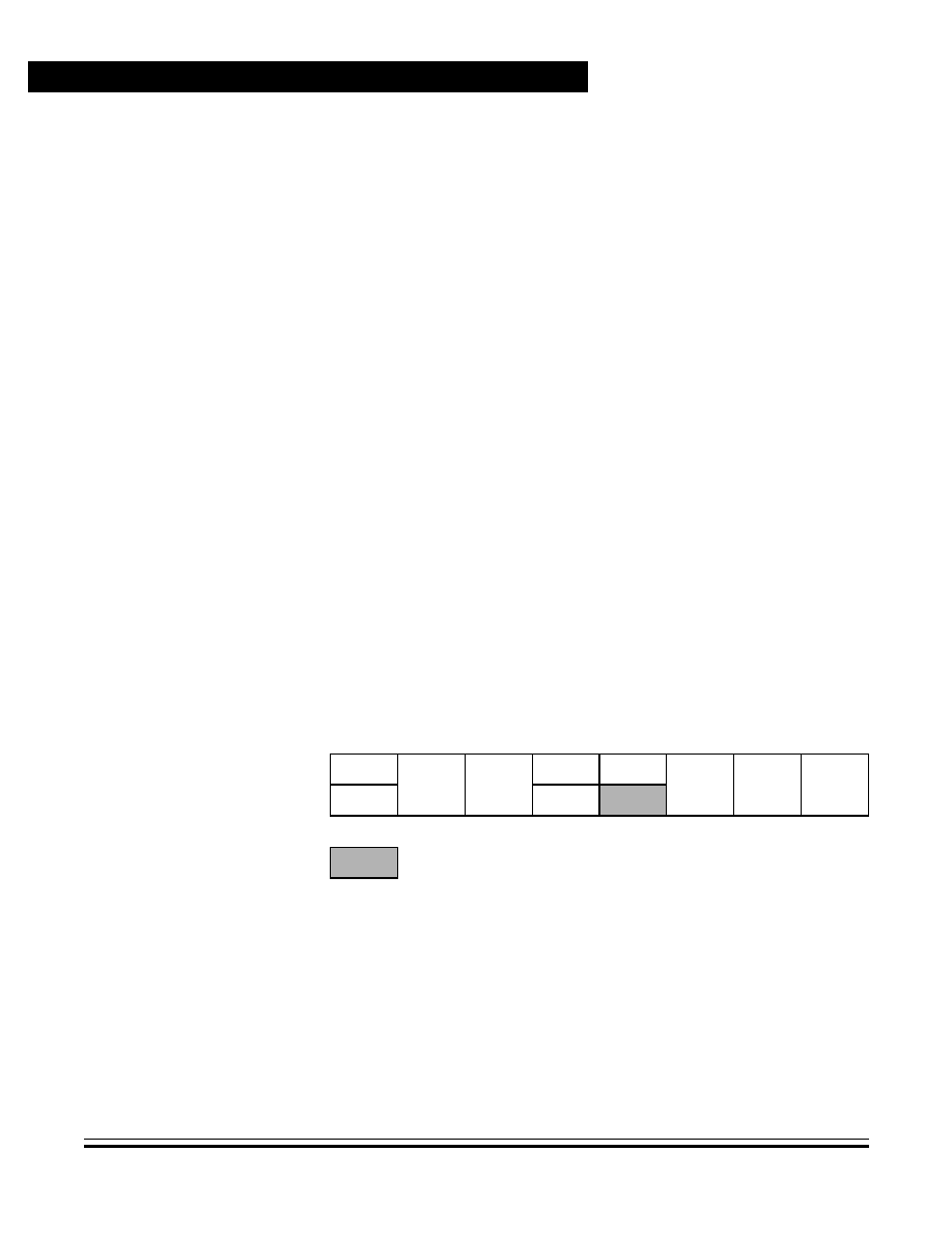
Timer Interface Module (TIM)
Advance Information
MC68HC908RK2
--
Rev. 4.0
208
Timer Interface Module (TIM)
MOTOROLA
15.9 I/O Registers
These I/O registers control and monitor operation of the TIM:
∑
TIM status and control register, TSC
∑
TIM control registers, TCNTH and TCNTL
∑
TIM counter modulo registers, TMODH and TMODL
∑
TIM channel status and control registers, TSC0 and TSC1
∑
TIM channel registers, TCH0H, TCH0L, TCH1H, and TCH1L
15.9.1 TIM Status and Control Register
The TIM status and control register (TSC):
∑
Enables TIM overflow interrupts
∑
Flags TIM overflows
∑
Stops the TIM counter
∑
Resets the TIM counter
∑
Prescales the TIM counter clock
TOF -- TIM Overflow Flag Bit
This read/write flag is set when the TIM counter reaches the modulo
value programmed in the TIM counter modulo registers. Clear TOF by
reading the TIM status and control register when TOF is set and then
writing a logic 0 to TOF. If another TIM overflow occurs before the
Address:
$0020
Bit 7
6
5
4
3
2
1
Bit 0
Read:
TOF
TOIE
TSTOP
0
0
PS2
PS1
PS0
Write:
0
TRST
Reset:
0
0
1
0
0
0
0
0
= Unimplemented
Figure 15-4. TIM Status and Control Register (TSC)

Timer Interface Module (TIM)
I/O Registers
MC68HC908RK2
--
Rev. 4.0
Advance Information
MOTOROLA
Timer Interface Module (TIM)
209
clearing sequence is complete, then writing logic 0 to TOF has no
effect. Therefore, a TOF interrupt request cannot be lost due to
inadvertent clearing of TOF. Reset clears the TOF bit. Writing a
logic 1 to TOF has no effect.
1 = TIM counter has reached modulo value.
0 = TIM counter has not reached modulo value.
TOIE -- TIM Overflow Interrupt Enable Bit
This read/write bit enables TIM overflow interrupts when the TOF bit
becomes set. Reset clears the TOIE bit.
1 = TIM overflow interrupts enabled
0 = TIM overflow interrupts disabled
TSTOP -- TIM Stop Bit
This read/write bit stops the TIM counter. Counting resumes when
TSTOP is cleared. Reset sets the TSTOP bit, stopping the TIM
counter until software clears the TSTOP bit.
1 = TIM counter stopped
0 = TIM counter active
NOTE:
Do not set the TSTOP bit before entering wait mode if the TIM is required
to exit wait mode.
TRST -- TIM Reset Bit
Setting this write-only bit resets the TIM counter and the TIM
prescaler. Setting TRST has no effect on any other registers.
Counting resumes from $0000. TRST is cleared automatically after
the TIM counter is reset and always reads as logic 0. Reset clears the
TRST bit.
1 = Prescaler and TIM counter cleared
0 = No effect
NOTE:
Setting the TSTOP and TRST bits simultaneously stops the TIM counter
at a value of $0000.
PS2≠PS0 -- Prescaler Select Bits
These read/write bits select either the TCLK pin or one of the seven
prescaler outputs as the input to the TIM counter as
Table 15-2
shows. Reset clears the PS2≠PS0 bits.

Timer Interface Module (TIM)
Advance Information
MC68HC908RK2
--
Rev. 4.0
210
Timer Interface Module (TIM)
MOTOROLA
15.9.2 TIM Counter Registers
The two read-only TIM counter registers contain the high and low bytes
of the value in the TIM counter. Reading the high byte (TCNTH) latches
the contents of the low byte (TCNTL) into a buffer. Subsequent reads of
TCNTH do not affect the latched TCNTL value until TCNTL is read.
Reset clears the TIM counter registers. Setting the TIM reset bit (TRST)
also clears the TIM counter registers
NOTE:
If you read TCNTH during a break interrupt, be sure to unlatch TCNTL
by reading TCNTL before exiting the break interrupt. Otherwise, TCNTL
retains the value latched during the break.
Table 15-2. Prescaler Selection
PS2≠PS0
TIM Clock Source
000
Internal bus clock
˜
1
001
Internal bus clock
˜
2
010
Internal bus clock
˜
4
011
Internal bus clock
˜
8
100
Internal bus clock
˜
16
101
Internal bus clock
˜
32
110
Internal bus clock
˜
64
111
TCLK
Register Name and Address: TCNTH--$0021
Bit 7
6
5
4
3
2
1
Bit 0
Read:
Bit 15
14
13
12
11
10
9
Bit 8
Write:
Reset:
0
0
0
0
0
0
0
0
Register Name and Address: TCNTL--$0022
Bit 7
6
5
4
3
2
1
Bit 0
Read:
Bit 7
6
5
4
3
2
1
Bit 0
Write:
Reset:
0
0
0
0
0
0
0
0
= Unimplemented
Figure 15-5. TIM Counter Registers (TCNTH and TCNTL)

Timer Interface Module (TIM)
I/O Registers
MC68HC908RK2
--
Rev. 4.0
Advance Information
MOTOROLA
Timer Interface Module (TIM)
211
15.9.3 TIM Counter Modulo Registers
The read/write TIM modulo registers contain the modulo value for the
TIM counter. When the TIM counter reaches the modulo value, the
overflow flag (TOF) becomes set, and the TIM counter resumes counting
from $0000 at the next timer clock. Writing to the high byte (TMODH)
inhibits the TOF bit and overflow interrupts until the low byte (TMODL) is
written. Reset sets the TIM counter modulo registers.
NOTE:
Reset the TIM counter before writing to the TIM counter modulo registers.
15.9.4 TIM Channel Status and Control Registers
Each of the TIM channel status and control registers (TSC0 and TSC1):
∑
Flags input captures and output compares
∑
Enables input capture and output compare interrupts
∑
Selects input capture, output compare, or PWM operation
∑
Selects high, low, or toggling output on output compare
∑
Selects rising edge, falling edge, or any edge as the active input
capture trigger
∑
Selects output toggling on TIM overflow
∑
Selects 0 percent and 100 percent PWM duty cycle
∑
Selects buffered or unbuffered output compare/PWM operation
Register Name and Address: TMODH--$0023
Bit 7
6
5
4
3
2
1
Bit 0
Read:
Bit 15
14
13
12
11
10
9
Bit 8
Write:
Reset:
1
1
1
1
1
1
1
1
Register Name and Address: TMODL--$0024
Bit 7
6
5
4
3
2
1
Bit 0
Read:
Bit 7
6
5
4
3
2
1
Bit 0
Write:
Reset:
1
1
1
1
1
1
1
1
Figure 15-6. TIM Counter Modulo Registers (TMODH and TMODL)

Timer Interface Module (TIM)
Advance Information
MC68HC908RK2
--
Rev. 4.0
212
Timer Interface Module (TIM)
MOTOROLA
CHxF -- Channel x Flag Bit
When channel x is an input capture channel, this read/write bit is set
when an active edge occurs on the channel x pin. When channel x is
an output compare channel, CHxF is set when the value in the TIM
counter registers matches the value in the TIM channel x registers.
When TIM CPU interrupt requests are enabled (CHxIE = 1), clear
CHxF by reading TIM channel x status and control register with CHxF
set and then writing a logic 0 to CHxF. If another interrupt request
occurs before the clearing sequence is complete, then writing logic 0
to CHxF has no effect. Therefore, an interrupt request cannot be lost
due to inadvertent clearing of CHxF.
Reset clears the CHxF bit. Writing a logic 1 to CHxF has no effect.
1 = Input capture or output compare on channel x
0 = No input capture or output compare on channel x
CHxIE -- Channel x Interrupt Enable Bit
This read/write bit enables TIM CPU interrupts on channel x.
Reset clears the CHxIE bit.
1 = Channel x CPU interrupt requests enabled
0 = Channel x CPU interrupt requests disabled
Register Name and Address: TSC0--$0025
Bit 7
6
5
4
3
2
1
Bit 0
Read:
CH0F
CH0IE
MS0B
MS0A
ELS0B
ELS0A
TOV0
CH0MAX
Write:
0
Reset:
0
0
0
0
0
0
0
0
Register Name and Address: TSC1--$0028
Bit 7
6
5
4
3
2
1
Bit 0
Read:
CH1F
CH1IE
0
MS1A
ELS1B
ELS1A
TOV1
CH1MAX
Write:
0
Reset:
0
0
0
0
0
0
0
0
= Unimplemented
Figure 15-7. TIM Channel Status and Control Registers
(TSC0 and TSC1)

Timer Interface Module (TIM)
I/O Registers
MC68HC908RK2
--
Rev. 4.0
Advance Information
MOTOROLA
Timer Interface Module (TIM)
213
MSxB -- Mode Select Bit B
This read/write bit selects buffered output compare/PWM operation.
MSxB exists only in the TIM channel 0 and TIM channel 1 status and
control registers.
Setting MS0B disables the TIM channel 1 status and control register
and reverts TCH1 to general-purpose I/O.
Reset clears the MSxB bit.
1 = Buffered output compare/PWM operation enabled
0 = Buffered output compare/PWM operation disabled
MSxA -- Mode Select Bit A
When ELSxB:A
00, this read/write bit selects either input capture
operation or unbuffered output compare/PWM operation.
See
Table 15-3
.
1 = Unbuffered output compare/PWM operation
0 = Input capture operation
When ELSxB:A = 00, this read/write bit selects the initial output level
of the TCHx pin. See
Table 15-3
. Reset clears the MSxA bit.
1 = Initial output level low
0 = Initial output level high
NOTE:
Before changing a channel function by writing to the MSxB or MSxA bit,
set the TSTOP and TRST bits in the TIM status and control register
(TSC).
ELSxB and ELSxA -- Edge/Level Select Bits
When channel x is an input capture channel, these read/write bits
control the active edge-sensing logic on channel x.
When channel x is an output compare channel, ELSxB and ELSxA
control the channel x output behavior when an output compare
occurs.
When ELSxB and ELSxA are both clear, channel x is not connected
to port B, and pin PTBx/TCHx is available as a general-purpose I/O
pin.
Table 15-3
shows how ELSxB and ELSxA work. Reset clears the
ELSxB and ELSxA bits.

Timer Interface Module (TIM)
Advance Information
MC68HC908RK2
--
Rev. 4.0
214
Timer Interface Module (TIM)
MOTOROLA
NOTE:
Before enabling a TIM channel register for input capture operation, make
sure that the PTB/TCHx pin is stable for at least two bus clocks.
TOVx -- Toggle On Overflow Bit
When channel x is an output compare channel, this read/write bit
controls the behavior of the channel x output when the TIM counter
overflows. When channel x is an input capture channel, TOVx has no
effect. Reset clears the TOVx bit.
1 = Channel x pin toggles on TIM counter overflow.
0 = Channel x pin does not toggle on TIM counter overflow.
CHxMAX -- Channel x Maximum Duty Cycle Bit
When the TOVx bit is at logic 1 and clear output on compare is
selected, setting the CHxMAX bit forces the duty cycle of buffered and
unbuffered PWM signals to 100 percent. As
Figure 15-8
shows, the
Table 15-3. Mode, Edge, and Level Selection
MSxB:MSxA
ELSxB:ELSxA
Mode
Configuration
X0
00
Output preset
Pin under port control;
initial output level high
X1
00
Pin under port control;
initial output level low
00
01
Input capture
Capture on rising edge only
00
10
Capture on falling edge only
00
11
Capture on rising or
falling edge
01
01
Output
compare or
PWM
Toggle output on compare
01
10
Clear output on compare
01
11
Set output on compare
1X
01
Buffered output
compare or
buffered PWM
Toggle output on compare
1X
10
Clear output on compare
1X
11
Set output on compare
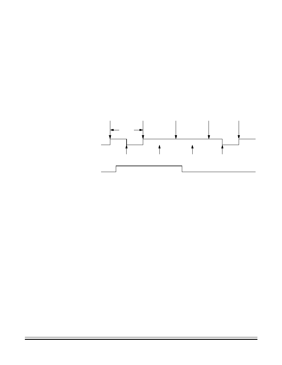
Timer Interface Module (TIM)
I/O Registers
MC68HC908RK2
--
Rev. 4.0
Advance Information
MOTOROLA
Timer Interface Module (TIM)
215
CHxMAX bit takes effect in the cycle after it is set or cleared. The
output stays at 100 percent duty cycle level until the cycle after
CHxMAX is cleared.
NOTE:
The PWM 0 percent duty cycle is defined as output low all of the time.
To generate the 0 percent duty cycle, select clear output on compare
and then clear the TOVx bit (CHxMAX = 0). The PWM 100 percent duty
cycle is defined as output high all of the time. To generate the 100
percent duty cycle, use the CHxMAX bit in the TSCx register.
Figure 15-8. CHxMAX Latency
15.9.5 TIM Channel Registers
These read/write registers contain the captured TIM counter value of the
input capture function or the output compare value of the output
compare function. The state of the TIM channel registers after reset is
unknown.
In input capture mode (MSxB:MSxA = 0:0), reading the high byte of the
TIM channel x registers (TCHxH) inhibits input captures until the low
byte (TCHxL) is read.
In output compare mode (MSxB:MSxA
0:0), writing to the high byte of
the TIM channel x registers (TCHxH) inhibits output compares until the
low byte (TCHxL) is written.
OUTPUT
OVERFLOW
PTBx/TCHx
PERIOD
CHxMAX
OVERFLOW
OVERFLOW
OVERFLOW
OVERFLOW
COMPARE
OUTPUT
COMPARE
OUTPUT
COMPARE
OUTPUT
COMPARE
Timer Interface Module (TIM)
Advance Information
MC68HC908RK2
--
Rev. 4.0
216
Timer Interface Module (TIM)
MOTOROLA
Register Name and Address: TCH0H--$0026
Bit 7
6
5
4
3
2
1
Bit 0
Read:
Bit 15
14
13
12
11
10
9
Bit 8
Write:
Reset:
Indeterminate after reset
Register Name and Address: TCH0L--$0027
Bit 7
6
5
4
3
2
1
Bit 0
Read:
Bit 7
6
5
4
3
2
1
Bit 0
Write:
Reset:
Indeterminate after reset
Figure 15-9. TIM Channel 0 Registers (TCH0H and TCH0L)
Register Name and Address: TCH1H--$0029
Bit 7
6
5
4
3
2
1
Bit 0
Read:
Bit 15
14
13
12
11
10
9
Bit 8
Write:
Reset:
Indeterminate after reset
Register Name and Address: TCH1L--$002A
Bit 7
6
5
4
3
2
1
Bit 0
Read:
Bit 7
6
5
4
3
2
1
Bit 0
Write:
Reset:
Indeterminate after reset
Figure 15-10. TIM Channel 1 Registers (TCH1H and TCH1L)

MC68HC908RK2
--
Rev. 4.0
Advance Information
MOTOROLA
Preliminary Electrical Specifications
217
Advance Information -- MC68HC908RK2
Section 16. Preliminary Electrical Specifications
16.1 Contents
16.2
Introduction . . . . . . . . . . . . . . . . . . . . . . . . . . . . . . . . . . . . . . . 217
16.3
Absolute Maximum Ratings . . . . . . . . . . . . . . . . . . . . . . . . . . 218
16.4
Functional Operating Range. . . . . . . . . . . . . . . . . . . . . . . . . . 219
16.5
Thermal Characteristics . . . . . . . . . . . . . . . . . . . . . . . . . . . . . 219
16.6
1.8-Volt to 3.3-Volt DC Electrical Characteristics . . . . . . . . . . 220
16.7
3.0-Volt DC Electrical Characteristics. . . . . . . . . . . . . . . . . . .221
16.8
2.0-Volt DC Electrical Characteristics . . . . . . . . . . . . . . . . . .222
16.9
Control Timing . . . . . . . . . . . . . . . . . . . . . . . . . . . . . . . . . . . . 223
16.10 Internal Oscillator Characteristics . . . . . . . . . . . . . . . . . . . . . . 223
16.11 LVI Characteristics . . . . . . . . . . . . . . . . . . . . . . . . . . . . . . . . . 224
16.12 Memory Characteristics . . . . . . . . . . . . . . . . . . . . . . . . . . . . . 225
16.2 Introduction
This section contains preliminary electrical and timing specifications.
NOTE:
The timing specifications, electrical, and thermal characteristic values
outlined in this section are design targets and have not yet been fully
tested.
Preliminary Electrical Specifications
Advance Information
MC68HC908RK2
--
Rev. 4.0
218
Preliminary Electrical Specifications
MOTOROLA
16.3 Absolute Maximum Ratings
Maximum ratings are the extreme limits to which the MCU can be
exposed without permanently damaging it.
NOTE:
This device is not guaranteed to operate properly at the maximum
ratings. Refer to
16.7 3.0-Volt DC Electrical Characteristics
for
guaranteed operating conditions.
NOTE:
This device contains circuitry to protect the inputs against damage due
to high static voltages or electric fields; however, it is advised that normal
precautions be taken to avoid application of any voltage higher than
maximum-rated voltages to this high-impedance circuit. For proper
operation, it is recommended that V
In
and V
Out
be constrained to the
range V
SS
(V
In
or V
Out
)
V
DD
. Reliability of operation is enhanced if
unused inputs are connected to an appropriate logic voltage level (for
example, either V
SS
or V
DD
.)
Characteristic
(1)
1. Voltages referenced to V
SS
.
Symbol
Value
Unit
Supply voltage
V
DD
≠0.3 to +3.6
V
Input voltage
V
In
V
SS
≠0.3 to V
DD
+0.3
V
Maximum current per pin
Excluding V
DD
, V
SS
,
and PTA7≠PTA0
I
±
15
mA
Maximum current for pins
PTA7≠PTA0
I
PTA7
≠I
PTA0
±
25
mA
Maximum current out of V
SS
I
MVSS
100
mA
Maximum current into V
DD
I
MVDD
100
mA
Storage temperature
T
STG
≠55 to +150
∞
C
Preliminary Electrical Specifications
Functional Operating Range
MC68HC908RK2
--
Rev. 4.0
Advance Information
MOTOROLA
Preliminary Electrical Specifications
219
16.4 Functional Operating Range
16.5 Thermal Characteristics
Characteristic
Symbol
Min
Max
Unit
Operating temperature range
(1)
1. Extended temperature range to be determined
T
A
≠40
85
∞
C
Operating voltage range
V
DD
1.8
3.6
V
Characteristic
Symbol
Value
Unit
Thermal resistance
SSOP (20 pin)
SOIC (20 pin)
JA
177
88
∞
C/W
I/O pin power dissipation
P
I/O
User determined
W
Power dissipation
(1)
1. Power dissipation is a function of temperature.
P
D
P
D
= (I
DD
x V
DD
) + P
I/O
=
K/(T
J
+ 273
∞
C)
W
Constant
(2)
2. K is a constant unique to the device. K can be determined for a known T
A
and measured
P
D.
With this value of K, P
D
and T
J
can be determined for any value of T
A
.
K
P
D
x
(T
A
+ 273
∞
C
)
+ P
D
2
x
JA
W/
∞
C
Average junction temperature
T
J
T
A
+ (P
D
x
JA
)
∞
C
Maximum junction temperature
T
JM
100
∞
C

Preliminary Electrical Specifications
Advance Information
MC68HC908RK2
--
Rev. 4.0
220
Preliminary Electrical Specifications
MOTOROLA
16.6 1.8-Volt to 3.3-Volt DC Electrical Characteristics
Characteristic
(1)
1. Parameters are design targets at V
DD
= 1.8 V to 3.3 V, V
SS
= 0 Vdc, T
A
= ≠40
∞
C to +85
∞
C, unless otherwise noted
Symbol
Min
Typ
(2)
2. Typical values reflect average measurements at midpoint of voltage range, 25
∞
C only.
Max
Unit
Output high voltage
(I
Load
= ≠1.2 mA)
(I
Load
= ≠2.0 mA)
V
OH
V
DD
≠0.3
V
DD
≠1.0
--
--
--
--
V
Output low voltage
(I
Load
= 1.2 mA)
(I
Load
= 3.0 mA)
(I
Load
= 3.0 mA) PTA7≠PTA0 only
V
OL
--
--
--
--
--
--
0.3
1.0
0.3
V
Input high voltage, all ports, IRQ1, OSC1
V
IH
0.7 x V
DD
--
V
DD
+ 0.3
V
Input low voltage, all ports, IRQ1, OSC1
V
IL
V
SS
--
0.3 x V
DD
V
V
DD
supply current
Run
(3)
(f
op
= 2.0 MHz)
Wait
(4)
(f
op
= 2.0 MHz)
Stop
(5)
25
∞
C
≠40
∞
C to 85
∞
C
25
∞
C with LVI enabled
≠40
∞
C to 85
∞
C with LVI enabled
3. Run (operating) I
DD
measured using internal clock generator module (f
op
= 2.0 MHz). V
DD
= 3.3 Vdc. All inputs 0.2 V from
rail. No dc loads. Less than 100 pF on all outputs. All ports configured as inputs. C
L
= 20 pF. OSC2 capacitance linearly
affects run I
DD
. Measured with all modules enabled.
4. Wait I
DD
measured using internal clock generator module, f
OP
= 2.0 MHz. All inputs 0.2 V from rail; no dc loads; less than
100 pF on all outputs. C
L
= 20 pF. OSC2 capacitance linearly affects wait I
DD
. All ports configured as inputs.
5. Stop I
DD
measured with no port pins sourcing current, all modules disabled except as noted.
I
DD
--
--
--
--
--
--
--
--
10
--
50
--
4.3
1.2
--
100
--
350
mA
mA
nA
nA
µ
A
µ
A
I/O ports high-impedance leakage current
(6)
6. Pullups and pulldowns are disabled.
I
IL
--
--
±
1
µ
A
Input current
I
In
--
--
±
1
µ
A
Capacitance
Ports (as input or output)
C
Out
C
In
--
--
--
--
12
8
pF
POR re-arm voltage
(7)
7. Maximum is highest voltage that POR is guaranteed.
V
POR
0
--
200
mV
POR reset voltage
(8)
8. Maximum is highest voltage that POR is possible.
V
POR
0
700
800
mV
POR rise time ramp rate
(9)
9. If minimum V
DD
is not reached before the internal POR reset is released, RST must be driven low externally until minimum
V
DD
is reached.
R
POR
0.02
--
--
V/ms
Monitor mode entry voltage
V
HI
V
DD
+ 2.5
--
8
V
Pullup resistor, PTA6≠PTA1, IRQ1
R
PU
50
--
120
k
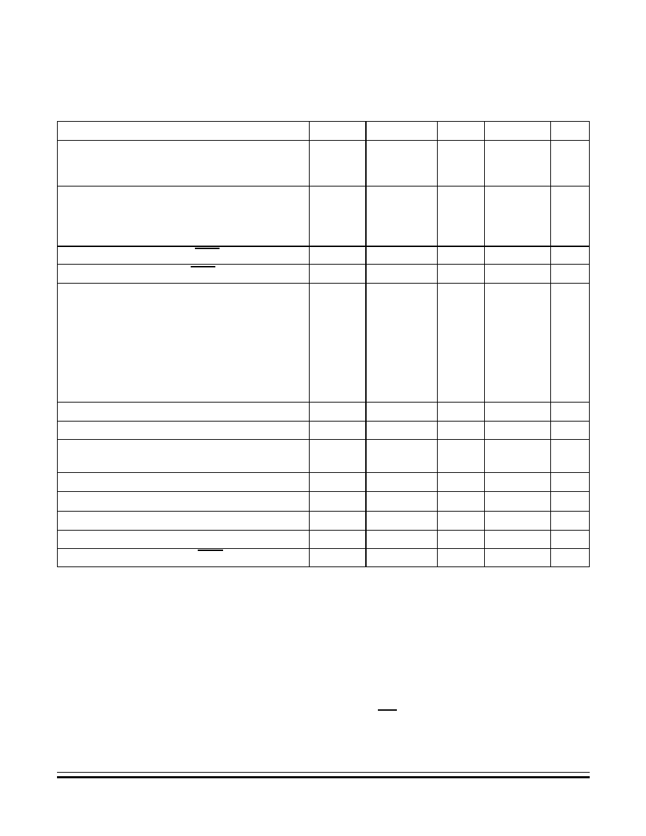
Preliminary Electrical Specifications
3.0-Volt DC Electrical Characteristics
MC68HC908RK2
--
Rev. 4.0
Advance Information
MOTOROLA
Preliminary Electrical Specifications
221
16.7 3.0-Volt DC Electrical Characteristics
Characteristic
(1)
1. Parameters are design targets at V
DD
= 3.0
±
10%, V
SS
= 0 Vdc, T
A
= ≠40
∞
C to +85
∞
C, unless otherwise noted
Symbol
Min
Typ
(2)
2. Typical values reflect average measurements at midpoint of voltage range, 25
∞
C only.
Max
Unit
Output high voltage
(I
Load
= ≠2.0 mA)
(I
Load
= ≠8.0 mA)
V
OH
V
DD
≠0.3
V
DD
≠1.0
--
--
--
--
V
Output low voltage
(I
Load
= 2.0 mA)
(I
Load
= 6.5 mA)
(I
Load
= 5.0 mA) PTA7≠PTA0 only
V
OL
--
--
--
--
--
--
0.3
1.0
0.3
V
Input high voltage, all ports, IRQ1, OSC1
V
IH
0.7 x V
DD
--
V
DD
+ 0.3
V
Input low voltage, all ports, IRQ1, OSC1
V
IL
V
SS
--
0.3 x V
DD
V
V
DD
supply current
Run
(3)
(f
op
= 4.0 MHz)
Wait
(4)
(f
op
= 4.0 MHz)
Stop
(5)
25
∞
C
≠40
∞
C to 85
∞
C
25
∞
C with LVI enabled
≠40
∞
C to 85
∞
C with LVI enabled
3. Run (operating) I
DD
measured using internal clock generator module (f
op
= 4.0 MHz). V
DD
= 3.3 Vdc. All inputs 0.2 V from
rail. No dc loads. Less than 100 pF on all outputs. All ports configured as inputs. C
L
= 20 pF. OSC2 capacitance linearly
affects run I
DD
. Measured with all modules enabled.
4. Wait I
DD
measured using internal clock generator module, f
OP
= 4.0 MHz. All inputs 0.2 V from rail; no dc loads; less than
100 pF on all outputs. C
L
= 20 pF. OSC2 capacitance linearly affects wait I
DD
. All ports configured as inputs.
5. Stop I
DD
measured with no port pins sourcing current, all modules disabled except as noted.
I
DD
--
--
--
--
--
--
--
--
10
--
50
--
8.6
1.2
--
100
--
350
mA
mA
nA
nA
µ
A
µ
A
I/O ports high-impedance leakage current
(6)
6. Pullups and pulldowns are disabled.
I
IL
--
--
±
1
µ
A
Input current
I
In
--
--
±
1
µ
A
Capacitance
Ports (as input or output)
C
Out
C
In
--
--
--
--
12
8
pF
POR re-arm voltage
(7)
7. Maximum is highest voltage that POR is guaranteed.
V
POR
0
--
200
mV
POR reset voltage
(8)
8. Maximum is highest voltage that POR is possible.
V
POR
0
700
800
mV
POR rise time ramp rate
(9)
9. If minimum V
DD
is not reached before the internal POR reset is released, RST must be driven low externally until minimum
V
DD
is reached.
R
POR
0.02
--
--
V/ms
Monitor mode entry voltage
V
HI
V
DD
+ 2.5
--
8
V
Pullup resistor, PTA6≠PTA1, IRQ1
R
PU
50
--
120
k
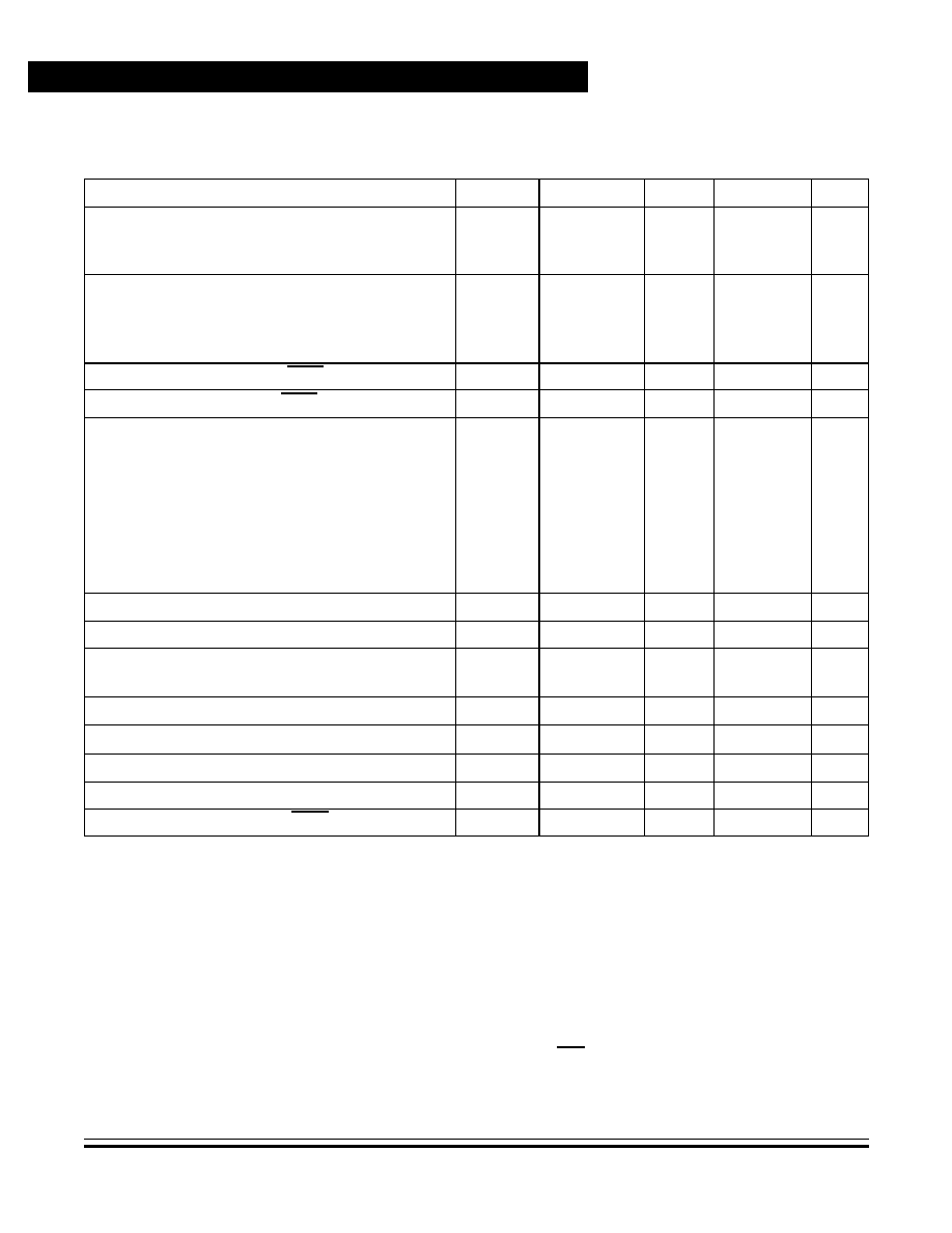
Preliminary Electrical Specifications
Advance Information
MC68HC908RK2
--
Rev. 4.0
222
Preliminary Electrical Specifications
MOTOROLA
16.8 2.0-Volt DC Electrical Characteristics
Characteristic
(1)
1. Parameters are design targets at V
DD
= 2.0
±
10%, V
SS
= 0 Vdc, T
A
= ≠40
∞
C to +85
∞
C, unless otherwise noted
Symbol
Min
Typ
(2)
2. Typical values reflect average measurements at midpoint of voltage range, 25
∞
C only.
Max
Unit
Output high voltage
(I
Load
= ≠1.2 mA)
(I
Load
= ≠2.0 mA)
V
OH
V
DD
≠0.3
V
DD
≠1.0
--
--
--
--
V
Output low voltage
(I
Load
= 1.2 mA)
(I
Load
= 3.0 mA)
(I
Load
= 3.0 mA) PTA7≠PTA0 only
V
OL
--
--
--
--
--
--
0.3
1.0
0.3
V
Input high voltage, all ports, IRQ1, OSC1
V
IH
0.7 x V
DD
--
V
DD
+ 0.3
V
Input low voltage, all ports, IRQ1, OSC1
V
IL
V
SS
--
0.3 x V
DD
V
V
DD
supply current
Run
(3)
(f
op
= 2.0 MHz)
Wait
(4)
(f
op
= 2.0 MHz)
Stop
(5)
25
∞
C
≠40
∞
C to 85
∞
C
25
∞
C with LVI enabled
≠40
∞
C to 85
∞
C with LVI enabled
3. Run (operating) I
DD
measured using internal clock generator module (f
op
= 2.0 MHz). V
DD
= 2.0 Vdc. All inputs 0.2 V from
rail. No dc loads. Less than 100 pF on all outputs. All ports configured as inputs. C
L
= 20 pF. OSC2 capacitance linearly
affects run I
DD
. Measured with all modules enabled.
4. Wait I
DD
measured using internal clock generator module, f
OP
= 2.0 MHz. All inputs 0.2 V from rail; no dc loads; less than
100 pF on all outputs. C
L
= 20 pF. OSC2 capacitance linearly affects wait I
DD
. All ports configured as inputs.
5. Stop I
DD
measured with no port pins sourcing current, all modules disabled except as noted.
I
DD
--
--
--
--
--
--
--
--
10
--
50
--
2.5
850
--
100
--
350
mA
µ
A
nA
nA
µ
A
µ
A
I/O ports high-impedance leakage current
(6)
6. Pullups and pulldowns are disabled.
I
IL
--
--
±
1
µ
A
Input current
I
In
--
--
±
1
µ
A
Capacitance
Ports (as input or output)
C
Out
C
In
--
--
--
--
12
8
pF
POR re-arm voltage
(7)
7. Maximum is highest voltage that POR is guaranteed.
V
POR
0
--
200
mV
POR reset voltage
(8)
8. Maximum is highest voltage that POR is possible.
V
POR
0
700
800
mV
POR rise time ramp rate
(9)
9. If minimum V
DD
is not reached before the internal POR reset is released, RST must be driven low externally until minimum
V
DD
is reached.
R
POR
0.02
--
--
V/ms
Monitor mode entry voltage
V
HI
V
DD
+ 2.5
--
8
V
Pullup resistor, PTA6≠PTA1, IRQ1
R
PU
50
--
120
k

Preliminary Electrical Specifications
Control Timing
MC68HC908RK2
--
Rev. 4.0
Advance Information
MOTOROLA
Preliminary Electrical Specifications
223
16.9 Control Timing
16.10 Internal Oscillator Characteristics
Characteristic
Symbol
Min
Max
Unit
Bus operating frequency
V
DD
= 3.0 V
±
10%
V
DD
= 2.0 V
±
10%
f
BUS
32k
32k
4.0 M
2.0 M
Hz
RESET pulse width low
t
RL
1.5
--
t
cyc
IRQ interrupt pulse width low (edge-triggered)
t
ILHI
1.5
--
t
cyc
IRQ interrupt pulse period
t
ILIL
Note 4
--
t
cyc
16-bit timer (Note 2)
Input capture pulse width (Note 3)
Input capture period
Input clock pulse width
t
TH,
t
TL
t
TLTL
t
TCH
, t
TCL
2
Note 4
(1/f
OP
) + 5
--
--
--
t
cyc
t
cyc
ns
Notes:
1. V
DD
= 1.8 V to 3.3 V, V
SS
= 0 Vdc, T
A
= ≠40
∞
C to +85
∞
C, unless otherwise noted
2. The 2-bit timer prescaler is the limiting factor in determining timer resolution.
3. Refer to
Table 15-3. Mode, Edge, and Level Selection
and supporting note.
4. The minimum period t
TLTL
or t
ILIL
should not be less than the number of cycles it takes to execute the capture interrupt
service routine plus 2 t
cyc
.
Characteristic
(1)
Symbol
Min
Typ
Max
Unit
Internal oscillator base frequency without
trim
(2)
(3)
f
INTOSC
230.4
307.2
384.0
kHz
Internal oscillator base frequency with trim
(2)
(3)
f
INTOSC(I)
291.8
307.2
322.6
kHz
Internal oscillator multiplier
(4)
N
1
--
127
--
External clock option
(5)
3 V
±
10%
2 V
±
10%
f
EXTOSC
128 k
128 k
--
--
16
8
MHz
1. V
DD
= 1.8 V to 3.3 V, V
SS
= 0 Vdc, T
A
= ≠40
∞
C to +85
∞
C, unless otherwise noted
2. Internal oscillator is selectable through software for a maximum frequency,. Actual frequency will be multiplier (N) x base
frequency.
3. f
BUS
= (f
INTOSC
/ 4) x (internal oscillator multiplier)
4. Multiplier must be chosen to limit the maximum bus frequency to the maximum listed in
16.9 Control Timing
.
5. No more than 10% duty cycle deviation from 50%

Preliminary Electrical Specifications
Advance Information
MC68HC908RK2
--
Rev. 4.0
224
Preliminary Electrical Specifications
MOTOROLA
16.11 LVI Characteristics
Characteristic
(1)
1. The LVI samples V
DD
, V
LVR
, and V
LVS
are V
DD
voltages.
2.
Symbol
Min
Typ
Max
Unit
LVI low battery sense voltage
(1)
V
LVS
1.90
2.00
2.15
V
LVI trip voltage
(1)
V
LVR
1.76
1.85
2.00
V
LVI trip voltage hysteresis
H
LVR
50
70
90
mV
V
DD
slew rate -- rising
SR
R
--
--
0.05
V/
µ
s
V
DD
slew rate -- falling
SR
F
--
--
0.10
V/
µ
s
Response time -- SR
SR
max
t
resp
--
--
6.0
µ
s
Response time -- SR > SR
max
t
resp
--
--
See Note 2
µ
s
Enable time (enable to output transition)
t
en
--
--
50
uS
V
D D
V
LVR
≠
SR
m ax
------------------------------------
V
D D
V
L VR
≠
SR
------------------------------------
≠
1.5
+
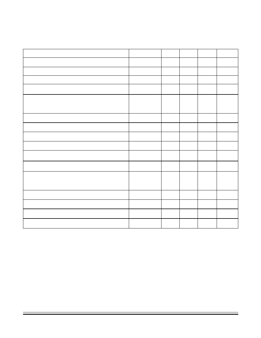
Preliminary Electrical Specifications
Memory Characteristics
MC68HC908RK2
--
Rev. 4.0
Advance Information
MOTOROLA
Preliminary Electrical Specifications
225
16.12 Memory Characteristics
Characteristic
Symbol
Min
Typ
Max
Unit
RAM data retention voltage
V
RDR
1.3
--
--
V
FLASH pages per row
--
8
--
8
Pages
FLASH bytes per page
--
1
--
1
Bytes
FLASH read bus clock frequency
f
Read
(1)
1. f
READ
is defined as the frequency range for which the FLASH memory can be read.
32 K
--
2.5 M
Hz
FLASH charge pump clock frequency
(see
4.5 FLASH 2TS Charge Pump Frequency
Control
)
f
Pump
(2)
2. f
Pump
is defined as the charge pump clock frequency required for program, erase, and margin read operations.
1.8
--
2.5
MHz
FLASH block/bulk erase time
t
Erase
100
--
--
ms
FLASH row erase time
t
RowErase
30
--
--
ms
FLASH high voltage kill time
t
Kill
200
--
--
µ
s
FLASH return to read time
t
HVD
50
--
--
µ
s
FLASH page program pulses
fls
Pulses
(3)
3. fls
Pulses
is defined as the number of pulses used to program the FLASH using the required smart program algorithm.
--
--
15
Pulses
FLASH page program step size
t
Step
(4)
4. t
Step
is defined as the amount of time during one page program cycle that HVEN is held high.
1.0
--
1.2
ms
FLASH cumulative program time per row between
erase cycles
t
Row
(5)
5. t
Row
is defined as the cumulative time a row can see the program voltage before the row must be erased before further
programming.
--
--
8
Page
program
cycles
FLASH HVEN low to MARGIN high time
t
HVTV
50
--
--
µ
s
FLASH MARGIN high to PGM low time
t
VTP
150
--
--
µ
s
FLASH 2TS row program endurance
(6)
6. The minimum row endurance value specifies each row of the FLASH 2TS memory is guaranteed to work for at least this
many erase/program cycles.
--
10
4
---
---
Cycles
FLASH data retention time
(7)
7. The FLASH is guaranteed to retain data over the entire temperature range for at least the minimum time specified.
--
10
---
---
Years

Preliminary Electrical Specifications
Advance Information
MC68HC908RK2
--
Rev. 4.0
226
Preliminary Electrical Specifications
MOTOROLA

MC68HC908RK2
--
Rev. 4.0
Advance Information
MOTOROLA
Mechanical Specifications
227
Advance Information -- MC68HC908RK2
Section 17. Mechanical Specifications
17.1 Contents
17.2
Introduction . . . . . . . . . . . . . . . . . . . . . . . . . . . . . . . . . . . . . . . 227
17.3
20-Pin Plastic SSOP Package (Case No. 940C-03). . . . . . . . 228
17.4
20-Pin SOIC Plastic Package (Case No. 751D-05) . . . . . . . . 228
17.2 Introduction
This section gives the dimensions for:
∑
20-pin SSOP package (case 940C-03)
∑
20-pin SOIC (case 751D-05)
The following figures show the latest package drawings at the time of this
publication. To make sure that you have the latest package
specifications, contact one of the following:
∑
Local Motorola Sales Office
∑
Worldwide Web (wwweb) at
http://www.motorola.com/semiconductors/
Follow Worldwide Web on-line instructions to retrieve the current
mechanical specifications.
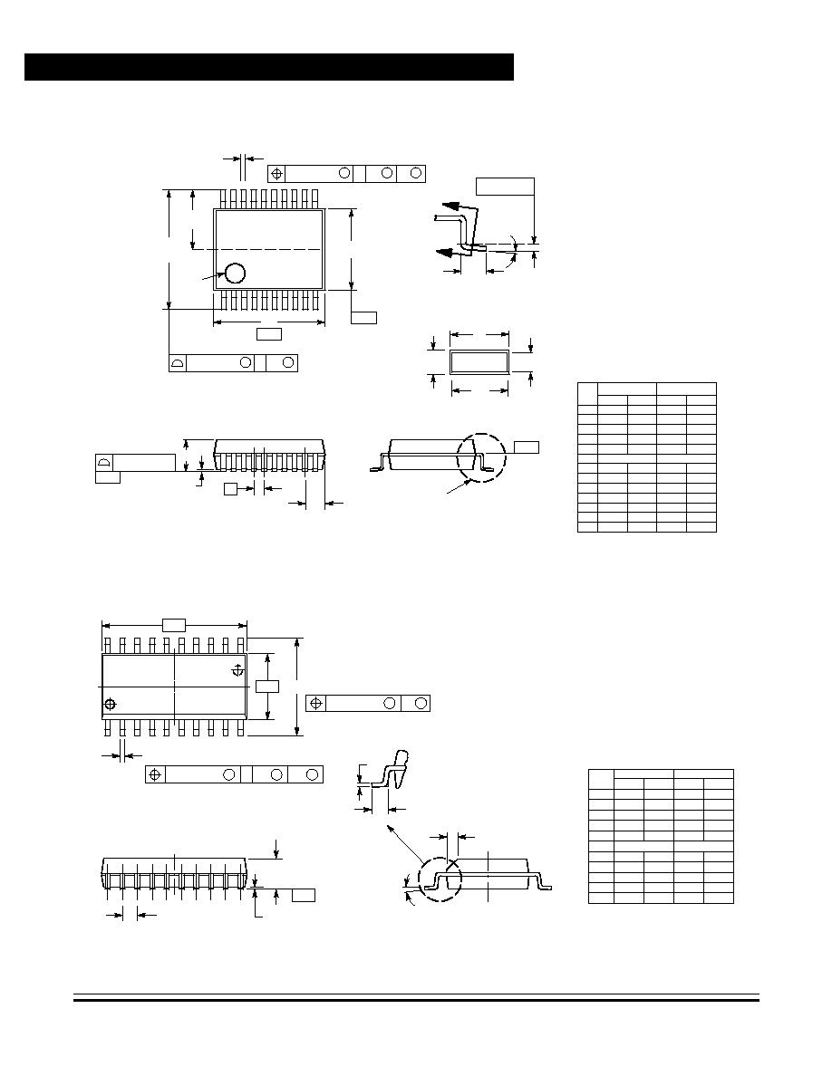
Mechanical Specifications
Advance Information
MC68HC908RK2
--
Rev. 4.0
228
Mechanical Specifications
MOTOROLA
17.3 20-Pin Plastic SSOP Package (Case No. 940C-03)
17.4 20-Pin SOIC Plastic Package (Case No. 751D-05)
20
11
10
1
H
A
B
F
M
K
20X REF
S
U
M
0.12 (0.005)
V
S
T
L
L/2
PIN 1
IDENT
S
U
M
0.20 (0.008)
T
≠V≠
≠U≠
D
C
0.076 (0.003)
G
≠T≠
SEATING
PLANE
DETAIL E
N
N
0.25 (0.010)
««««
««««
…………
…………
K
J
J1
K1
SECTION N≠N
DIM
A
MIN
MAX
MIN
MAX
INCHES
7.07
7.33
0.278
0.288
MILLIMETERS
B
5.20
5.38
0.205
0.212
C
1.73
1.99
0.068
0.078
D
0.05
0.21
0.002
0.008
F
0.63
0.95
0.024
0.037
G
0.65 BSC
0.026 BSC
H
0.59
0.75
0.023
0.030
J
0.09
0.20
0.003
0.008
J1
0.09
0.16
0.003
0.006
K
0.25
0.38
0.010
0.015
K1
0.25
0.33
0.010
0.013
_
_
_
_
NOTES:
1. DIMENSIONING AND TOLERANCING PER ANSI
Y14.5M, 1982.
2. CONTROLLING DIMENSION: MILLIMETER.
3. DIMENSION A DOES NOT INCLUDE MOLD
FLASH, PROTRUSIONS OR GATE BURRS. MOLD
FLASH OR GATE BURRS SHALL NOT EXCEED
0.15 (0.006) PER SIDE.
4. DIMENSION B DOES NOT INCLUDE INTERLEAD
FLASH OR PROTRUSION. INTERLEAD FLASH OR
PROTRUSION SHALL NOT EXCEED 0.15 (0.006)
PER SIDE.
5. DIMENSION K DOES NOT INCLUDE DAMBAR
PROTRUSION/INTRUSION. ALLOWABLE
DAMBAR PROTRUSION SHALL BE 0.13 (0.005)
TOTAL IN EXCESS OF K DIMENSION AT
MAXIMUM MATERIAL CONDITION. DAMBAR
INTRUSION SHALL NOT REDUCE DIMENSION K
BY MORE THAN 0.07 (0.002) AT LEAST MATERIAL
CONDITION.
6. TERMINAL NUMBERS ARE SHOWN FOR
REFERENCE ONLY.
7. DIMENSION A AND B ARE TO BE DETERMINED
AT DATUM PLANE ≠W≠.
L
7.65
7.90
0.301
0.311
M
0
8
0
8
DETAIL E
≠W≠
MIN
MIN
MAX
MAX
MILLIMETERS
INCHES
DIM
A
B
C
D
F
G
J
K
M
P
R
0.510
0.299
0.104
0.019
0.035
0.012
0.009
7
∞
0.415
0.029
0.499
0.292
0.093
0.014
0.020
0.010
0.004
0
∞
0.395
0.010
12.95
7.60
2.65
0.49
0.90
0.32
0.25
7
∞
10.55
0.75
12.65
7.40
2.35
0.35
0.50
0.25
0.10
0
∞
10.05
0.25
NOTES:
1. DIMENSIONING AND TOLERANCING PER
ANSI Y14.5M, 1982.
2. CONTROLLING DIMENSION: MILLIMETER.
3. DIMENSIONS A AND B DO NOT INCLUDE
MOLD PROTRUSION.
4. MAXIMUM MOLD PROTRUSION 0.150
(0.006) PER SIDE.
5. DIMENSION D DOES NOT INCLUDE
DAMBAR PROTRUSION. ALLOWABLE
DAMBAR PROTRUSION SHALL BE 0.13
(0.005) TOTAL IN EXCESS OF D DIMENSION
AT MAXIMUM MATERIAL CONDITION.
1.27 BSC
0.050 BSC
-A-
-B-
P
10 PL
1
10
11
20
-T-
D
20 PL
K
C
SEATING
PLANE
R
X 45
∞
M
0.010 (0.25)
B
M
M
0.010 (0.25)
T A
B
M
S
S
G
18 PL
F
J

MC68HC908RK2 -- Rev. 4.0
Advance Information
MOTOROLA
Ordering Information
229
Advance Information -- MC68HC908RK2
Section 18. Ordering Information
18.1 Contents
18.2
Introduction . . . . . . . . . . . . . . . . . . . . . . . . . . . . . . . . . . . . . . . 229
18.3
MC Order Numbers . . . . . . . . . . . . . . . . . . . . . . . . . . . . . . . .229
18.2 Introduction
This section contains ordering numbers for the MC68HC908RK2.
18.3 MC Order Numbers
Table 18-1. MC Order Numbers
MC Order Number
(1)
1. DW = SOIC
SD =SSOP
Operating
Temperature Range
MC68HC908RK2CDW
≠40
∞
C to +85
∞
C
MC68HC908RK2CSD
≠40
∞
C to +85
∞
C

Advance Information
MC68HC908RK2 -- Rev. 4.0
230
Ordering Information
MOTOROLA
Ordering Information

blank

MC68HC908RK2/D
REV 4
MC
68HC08A
S60
T
echnical Data
How to Reach Us:
USA/EUROPE/LOCATIONS NOT LISTED:
Motorola Literature Distribution
P.O. Box 5405
Denver, Colorado 80217
1-303-675-2140
1-800-441-2447
TECHNICAL INFORMATION CENTER:
1-800-521-6274
JAPAN:
Motorola Japan Ltd.
SPS, Technical Information Center
3-20-1, Minami-Azabu, Minato-ku
Tokyo 106-8573 Japan
81-3-3440-3569
ASIA/PACIFIC:
Motorola Semiconductors H.K. Ltd.
Silicon Harbour Centre
2 Dai King Street
Tai Po Industrial Estate
Tai Po, N.T., Hong Kong
852-26668334
HOME PAGE:
http://www.motorola.com/semiconductors/
Q4/00
REV 1