 | Электронный компонент: MC12040P | Скачать:  PDF PDF  ZIP ZIP |

Device
Operating
Temperature Range
Package
MC12040
SEMICONDUCTOR
TECHNICAL DATA
PHASE¡FREQUENCY
DETECTOR
ORDERING INFORMATION
MC12040P
TA = 0
░
to +75
░
C
Plastic
FN SUFFIX
PLASTIC PACKAGE
CASE 775
(PLCC)
PIN CONNECTIONS
Order this document by MC12040/D
3
19
4
8
Not Recommended for New Designs
14
1
P SUFFIX
PLASTIC PACKAGE
CASE 646
Vref
NC
Compensation
(Top View)
NC
Voltage Feedback
NC
Current Sense
NC
RT/CT
VCC
VC
Output
Gnd
Power Ground
1
2
3
4
14
13
12
11
5
6
7
10
9
8
Phase-Frequency Detector
The MC12040 is a phase¡frequency detector intended for use in systems
requiring zero phase and frequency difference at lock. In combination with a
voltage controlled oscillator (such as the MC1648, MC12147, MC12148 or
MC12149), it is useful in a broad range of phase¡locked loop applications.
╖
Operating Frequency = 80 MHz Typical
Pin Conversion Table
14 PIN DIP
1
2
3
4
5
6
7
8
9
10
11
12
13
14
20 PIN PLCC
2
3
4
6
8
9
10
12
13
14
16
18
19
20
LOGIC DIAGRAM
R
S
Q
S
R Q
R 6
V 9
4 U (fR>fV)
3 U (fR>fV)
12 D (fV>fR)
11 D (fV>fR)
VCC1 = Pin 1
VCC2 = Pin 14
VEE = Pin 7
TRUTH TABLE
This is not strictly a functional truth table; i.e., it does not cover all possible
modes of operation. However, it gives a sufficient number of tests to
ensure that the device will function properly in all modes of operation.
0
0
1
0
R
1
0
1
1
1
1
1
1
1
0
1
0
1
1
1
V
1
1
1
0
1
0
1
0
1
1
1
X
X
X
X
U
1
1
1
1
0
0
0
0
0
0
0
X
X
X
X
D
0
0
0
0
0
0
1
1
1
1
0
X
X
X
X
U
0
0
0
0
1
1
1
1
1
1
1
X
X
X
X
D
1
1
1
1
1
1
0
0
0
0
1
Inputs
Outputs
⌐
Motorola, Inc. 1997
Rev 3

MC12040
2
MOTOROLA RF/IF DEVICE DATA
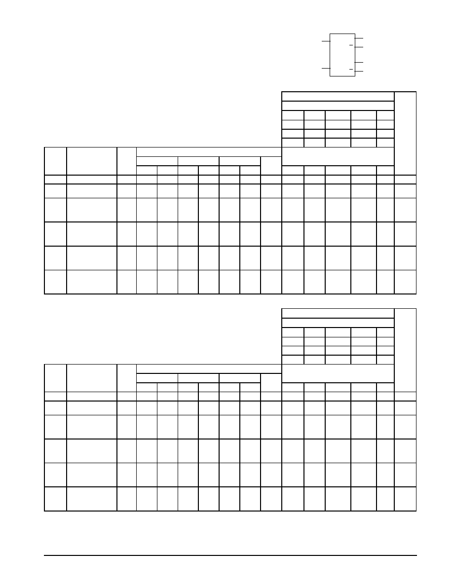
ELECTRICAL CHARACTERISTICS
The MC12040 has been designed to meet the dc
specifications shown in the test table after thermal
equilibrium has been established. Outputs are terminated
through a 50 ohm resistor to +3.0 V for +5.0 V tests and
through a 50 ohm resistor to ¡2.0 V for ¡5.2 V tests.
6
R
9
V
U
4
D
12
D
11
U
3
TEST VOLTAGE VALUES
(Volts)
@ Test Temperature
VIHmax
VILmin
VIHAmin
VILAmax
VEE
0
░
C
¡0.840
¡1.870
¡1.145
¡1.490
¡5.2
25
░
C
¡0.810
¡1.850
¡1.105
¡1.475
¡5.2
Supply Voltage = ¡5.2V
75
░
C
¡0.720
¡1.830
¡1.045
¡1.450
¡5.2
Pi
MC12040
TEST VOLTAGE APPLIED TO PINS BELOW
Pin
Under
0
░
C
25
░
C
75
░
C
TEST VOLTAGE APPLIED TO PINS BELOW
(VCC)
Symbol
Characteristics
Under
Test
Min
Max
Min
Max
Min
Max
Unit
VIHmax
VILmin
VIHAmin
VILAmax
VEE
(VCC)
Gnd
IE
Power Supply Drain
7
¡120
¡60
mAdc
7
1,14
IINH
Input Current
6
9
350
350
╡
Adc
6
9
7
7
1,14
1,14
VOH
1
Logic "1"
Output Voltage
3
4
11
12
¡1.000
¡0.840
¡0.960
¡0.810
¡0.900
¡0.720
Vdc
7
1,14
VOL
1
Logic "0"
Output Voltage
3
4
11
12
¡1.870
¡1.635
¡1.850
¡1.620
¡1.830
¡1.595
Vdc
7
1,14
VOHA
2
Logic "1"
Input Voltage
3
4
11
12
¡1.020
¡0.980
¡0.920
Vdc
6.9
7
1,14
VOLA
2
Logic "0"
Input Voltage
3
4
11
12
¡1.615
¡1.600
¡1.575
Vdc
9
6
9
6
6
9
6
9
7
1,14
TEST VOLTAGE VALUES
(Volts)
@ Test Temperature
VIHmax
VILmin
VIHAmin
VILAmax
VEE
0
░
C
+4.160
+3.130
+3.855
+3.510
+5.0
25
░
C
+4.190
+3.150
+3.895
+3.525
+5.0
Supply Voltage = +5.0V
75
░
C
+4.280
+3.170
+3.955
+3.550
+5.0
Pi
MC12040
TEST VOLTAGE APPLIED TO PINS BELOW
Pin
Under
0
░
C
25
░
C
75
░
C
TEST VOLTAGE APPLIED TO PINS BELOW
(VCC)
Symbol
Characteristics
Under
Test
Min
Max
Min
Max
Min
Max
Unit
VIHmax
VILmin
VIHAmin
VILAmax
VEE
(VCC)
Gnd
IE
Power Supply Drain
7
¡115
¡60
mAdc
1,14
7
IINH
Input Current
6
9
350
350
╡
Adc
6
9
1,14
1,14
7
7
VOH
1
Logic "1"
Output Voltage
3
4
11
12
4.000
4.160
4.040
4.190
4.100
4.280
Vdc
1,14
7
VOL
1
Logic "0"
Output Voltage
3
4
11
12
3.190
3.430
3.210
3.440
3.230
3.470
Vdc
1,14
7
VOHA
2
Logic "1"
Input Voltage
3
4
11
12
3.980
4.020
4.080
Vdc
6.9
1,14
7
VOLA
2
Logic "0"
Input Voltage
3
4
11
12
3.450
3.460
3.490
Vdc
9
6
9
6
6
9
6
9
1,14
7
NOTE: For more information on using an ECL device in a
+5V system, refer to Motorola Application Note
AN1406/D, "Designing with PECL (ECL at +5.0V)"

MC12040
3
MOTOROLA RF/IF DEVICE DATA
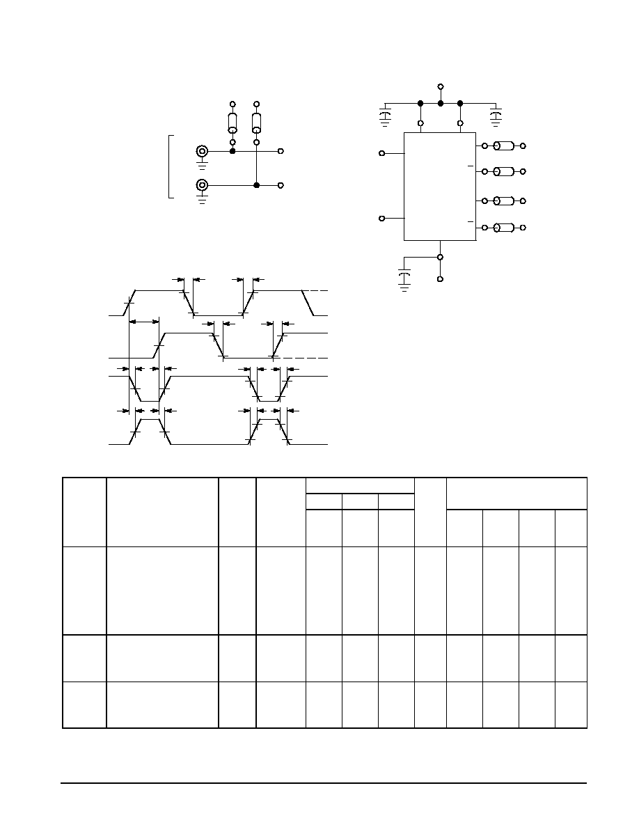
Figure 1. AC Tests
NOTES:
1 All input and output cables to the scope are equal lengths of 50
coaxial cable.
2 Unused input and outputs are connected to a 50
resistor to
ground.
3 The device under test must be preconditioned before performing
the ac tests. Preconditioning may be accomplished by applying
pulse generator 1 for a minimum of two pulses prior to pulse gen-
erator 2. The device must be preconditioned again when inputs to
pins 6 and 9 are interchanged. The same technique applies.
50%
Pulse
Gen 1
6
R
9
V
U
4
D
12
D
11
U
3
Pulse
Gen 1
Pulse
Gen 2
PRF = 5.0MHz
Duty Cycle = 50%
t+ = t¡ = 1.5ns
▒
0.2ns
To Scope Channel A
To Scope Channel B
7
VEE = ¡3.2 or ¡3.0V
0.1
╡
F
5.0
╡
F
0.1
╡
F
VCC = +2.0V
1
14
Pulse
Gen 2
Output
Waveform A
Output
Waveform B
50%
50%
50%
10%
90%
10%
90%
80%
20%
20%
80%
+1.1V
+1.1V
+0.3V
+0.3V
t+
t¡
t+
t¡
t+
t¡
t¡
t+
20ns
t+¡
t++
t++
t+¡
Pi
MC12040
TEST VOLTAGES/WAVEFORMS
Pi
0
░
C
25
░
C
85
░
C
APPLIED TO PINS LISTED
Symbol
Characteristic
Pin
Under
Test
Output
Waveform
Max
Max
Max
Unit
Pulse
Gen 1
Pulse
Gen 2
VEE
¡3.0 or
¡3.2V
VCC
+2.0V
t6+4+
t6+12+
t6+3¡
t6+11¡
t9+11+
t9+3+
t9+12¡
t9+4¡
Propagation Delay
6,4
6,12
6,3
6,11
9,11
9,3
9,12
9,4
B
A
A
B
B
A
A
B
4.6
6.0
4.5
6.4
4.6
6.0
4.5
6.4
4.6
6.0
4.5
6.4
4.6
6.0
4.5
6.4
5.0
6.6
4.9
7.0
5.0
6.6
4.9
7.0
ns
6
9
6
9
9
6
9
6
9
6
9
6
6
9
6
9
7
1,14
t3+
t4+
t11+
t14+
Output Rise Time
3
4
11
14
A
B
B
A
3.4
3.4
3.8
ns
6
6
9
9
9
9
6
6
7
1,14
t3¡
t4¡
t11¡
t14¡
Output Fall Time
3
4
11
14
A
B
B
A
3.4
3.4
3.8
ns
6
6
9
9
9
9
6
6
7
1,14

MC12040
4
MOTOROLA RF/IF DEVICE DATA
APPLICATIONS INFORMATION
The MC12040 is a logic network designed for use as a
phase comparator for MECL¡compatible input signals. It
determines the "lead" or "lag" phase relationship and the time
difference between the leading edges of the waveforms.
Since these edges occur only once per cycle, the detector
has a range of
▒
2
radians.
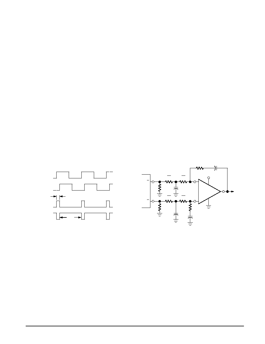
Operation of the device may be illustrated by assuming
two waveforms, R and V (Figure 2), of the same frequency
but differing in phase. If the logic had established by past
history that R was leading V, the U output of the detector (pin
4) would produce a positive pulse width equal to the phase
difference and the D output (pin 11 ) would simply remain low.
On the other hand, it is also possible that V was leading R
(Figure 2), giving rise to a positive pulse on the D output and
a constant low level on the U output pin. Both outputs for the
sample condition are valid since the determination of lead or
lag is dependent on past edge crossing and initial conditions
at start¡up. A stable phase¡locked loop will result from either
condition.
Phase error information is contained in the output duty
cycle¡that is, the ratio of the output pulse width to total
period. By integrating or low¡pass filtering the outputs of the
detector and shifting the level to accommodate ECL swings,
usable analog information for the voltage controlled oscillator
can be developed. A circuit useful for this function is shown in
Figure 3.
Proper level shifting is accomplished by differentially
driving the operational amplifier from the normally high
outputs of the phase detector (U and D). Using this technique
the quiescent differential voltage to the operational amplifier
is zero (assuming matched "1" levels from the phase
detector). The U and D outputs are then used to pass along
phase information to the operational amplifier. Phase error
summing is accomplished through resistors R1 connected to
the inputs of the operational amplifier. Some R¡C filtering
imbedded within the input network (NO TAG) may be very
beneficial since the very narrow correctional pulses of the
MC12040 would not normally be integrated by the amplifier.
Phase detector gain for this configuration is approximately
0.16 volts/radian.
System phase error stems from input offset voltage in the
operational amplifier, mismatching of nominally equal
resistors, and mismatching of phase detector "high" states
between the outputs used for threshold setting and phase
measuring. All these effects are reflected in the gain
constant. For example, a 16mV offset voltage in the amplifier
would cause an error of 0.016/ 0.16 = 0.1 radian or 5.7
degrees of error. Phase error can be trimmed to zero initially
by trimming either input offset or one of the threshold
resistors (R1 in Figure 3). Phase error over temperature
depends on how much the offending parameters drift.
Figure 2. Timing Diagram
Figure 3. Typical Filter and Summing Network
3
510
12
CC
¡
+
MC1741
510
CC
R1
2
R1
2
R1
2
R1
2
C
R2
MC12040
U
D
To
VCO
+10 to
+30V
R2
C
R Leads V
(D Output="0")
V Leads R
(D Output="0")
R
V
Lead
Lag

MC12040
5
MOTOROLA RF/IF DEVICE DATA
P SUFFIX
PLASTIC PACKAGE
CASE 646¡06
ISSUE M
1
7
14
8
B
A
DIM
MIN
MAX
MIN
MAX
MILLIMETERS
INCHES
A
0.715
0.770
18.16
18.80
B
0.240
0.260
6.10
6.60
C
0.145
0.185
3.69
4.69
D
0.015
0.021
0.38
0.53
F
0.040
0.070
1.02
1.78
G
0.100 BSC
2.54 BSC
H
0.052
0.095
1.32
2.41
J
0.008
0.015
0.20
0.38
K
0.115
0.135
2.92
3.43
L
M
¡¡¡
10 ¡¡¡
10
N
0.015
0.039
0.38
1.01
_
_
NOTES:
1. DIMENSIONING AND TOLERANCING PER ANSI
Y14.5M, 1982.
2. CONTROLLING DIMENSION: INCH.
3. DIMENSION L TO CENTER OF LEADS WHEN
FORMED PARALLEL.
4. DIMENSION B DOES NOT INCLUDE MOLD FLASH.
5. ROUNDED CORNERS OPTIONAL.
F
H
G
D
K
C
SEATING
PLANE
N
¡T¡
14 PL
M
0.13 (0.005)
L
M
J
0.290
0.310
7.37
7.87
OUTLINE DIMENSIONS
Motorola reserves the right to make changes without further notice to any products herein. Motorola makes no warranty, representation or guarantee regarding
the suitability of its products for any particular purpose, nor does Motorola assume any liability arising out of the application or use of any product or circuit, and
specifically disclaims any and all liability, including without limitation consequential or incidental damages. "Typical" parameters which may be provided in Motorola
data sheets and/or specifications can and do vary in different applications and actual performance may vary over time. All operating parameters, including "Typicals"
must be validated for each customer application by customer's technical experts. Motorola does not convey any license under its patent rights nor the rights of
others. Motorola products are not designed, intended, or authorized for use as components in systems intended for surgical implant into the body, or other
applications intended to support or sustain life, or for any other application in which the failure of the Motorola product could create a situation where personal injury
or death may occur. Should Buyer purchase or use Motorola products for any such unintended or unauthorized application, Buyer shall indemnify and hold Motorola
and its officers, employees, subsidiaries, affiliates, and distributors harmless against all claims, costs, damages, and expenses, and reasonable attorney fees
arising out of, directly or indirectly, any claim of personal injury or death associated with such unintended or unauthorized use, even if such claim alleges that
Motorola was negligent regarding the design or manufacture of the part. Motorola and
are registered trademarks of Motorola, Inc. Motorola, Inc. is an Equal
Opportunity/Affirmative Action Employer.
Mfax is a trademark of Motorola, Inc.
How to reach us:
USA / EUROPE / Locations Not Listed: Motorola Literature Distribution;
JAPAN: Nippon Motorola Ltd.: SPD, Strategic Planning Office, 141,
P.O. Box 5405, Denver, Colorado 80217. 1¡303¡675¡2140 or 1¡800¡441¡2447
4¡32¡1 Nishi¡Gotanda, Shagawa¡ku, Tokyo, Japan. 03¡5487¡8488
Customer Focus Center: 1¡800¡521¡6274
Mfax
TM
: RMFAX0@email.sps.mot.com ¡ TOUCHTONE 1¡602¡244¡6609
ASIA/PACIFIC: Motorola Semiconductors H.K. Ltd.; 8B Tai Ping Industrial Park,
Motorola Fax Back System
¡ US & Canada ONLY 1¡800¡774¡1848
51 Ting Kok Road, Tai Po, N.T., Hong Kong. 852¡26629298
¡ http://sps.motorola.com/mfax/
HOME PAGE: http://motorola.com/sps/
MC12040/D

