 | –≠–ª–µ–∫—Ç—Ä–æ–Ω–Ω—ã–π –∫–æ–º–ø–æ–Ω–µ–Ω—Ç: MJE15033 | –°–∫–∞—á–∞—Ç—å:  PDF PDF  ZIP ZIP |
1
Motorola Bipolar Power Transistor Device Data
Complementary Silicon Plastic
Power Transistors
. . . designed for use as high≠frequency drivers in audio amplifiers.
∑
DC Current Gain Specified to 5.0 Amperes
hFE = 50 (Min) @ IC = 0.5 Adc
hFE
= 10 (Min) @ IC = 2.0 Adc
∑
Collector≠Emitter Sustaining Voltage --
VCEO(sus)
= 250 Vdc (Min) -- MJE15032, MJE15033
∑
High Current Gain -- Bandwidth Product
fT = 30 MHz (Min) @ IC = 500 mAdc
∑
TO≠220AB Compact Package
ŒŒŒŒŒŒŒŒŒŒŒŒŒŒŒŒŒŒŒŒŒŒŒ
ŒŒŒŒŒŒŒŒŒŒŒŒŒŒŒŒŒŒŒŒŒŒŒ
MAXIMUM RATINGS
ŒŒŒŒŒŒŒŒŒŒŒŒ
Œ
ŒŒŒŒŒŒŒŒŒŒ
Œ
ŒŒŒŒŒŒŒŒŒŒŒŒ
Rating
ŒŒŒŒ
Œ
ŒŒ
Œ
ŒŒŒŒ
Symbol
ŒŒŒŒŒŒŒ
Œ
ŒŒŒŒŒ
Œ
ŒŒŒŒŒŒŒ
MJE15032
MJE15033
ŒŒŒ
Œ
Œ
Œ
ŒŒŒ
Unit
ŒŒŒŒŒŒŒŒŒŒŒŒ
ŒŒŒŒŒŒŒŒŒŒŒŒ
Collector≠Emitter Voltage
ŒŒŒŒ
ŒŒŒŒ
VCEO
ŒŒŒŒŒŒŒ
ŒŒŒŒŒŒŒ
250
ŒŒŒ
ŒŒŒ
Vdc
ŒŒŒŒŒŒŒŒŒŒŒŒ
ŒŒŒŒŒŒŒŒŒŒŒŒ
Collector≠Base Voltage
ŒŒŒŒ
ŒŒŒŒ
VCB
ŒŒŒŒŒŒŒ
ŒŒŒŒŒŒŒ
250
ŒŒŒ
ŒŒŒ
Vdc
ŒŒŒŒŒŒŒŒŒŒŒŒ
ŒŒŒŒŒŒŒŒŒŒŒŒ
Emitter≠Base Voltage
ŒŒŒŒ
ŒŒŒŒ
VEB
ŒŒŒŒŒŒŒ
ŒŒŒŒŒŒŒ
5.0
ŒŒŒ
ŒŒŒ
Vdc
ŒŒŒŒŒŒŒŒŒŒŒŒ
ŒŒŒŒŒŒŒŒŒŒŒŒ
Collector Current -- Continuous
-- Peak
ŒŒŒŒ
ŒŒŒŒ
IC
ŒŒŒŒŒŒŒ
ŒŒŒŒŒŒŒ
8.0
16
ŒŒŒ
ŒŒŒ
Adc
ŒŒŒŒŒŒŒŒŒŒŒŒ
ŒŒŒŒŒŒŒŒŒŒŒŒ
Base Current
ŒŒŒŒ
ŒŒŒŒ
IB
ŒŒŒŒŒŒŒ
ŒŒŒŒŒŒŒ
2.0
ŒŒŒ
ŒŒŒ
Adc
ŒŒŒŒŒŒŒŒŒŒŒŒ
Œ
ŒŒŒŒŒŒŒŒŒŒ
Œ
ŒŒŒŒŒŒŒŒŒŒŒŒ
Total Power Dissipation @ TC = 25
_
C
Derate above 25
_
C
ŒŒŒŒ
Œ
ŒŒ
Œ
ŒŒŒŒ
PD
ŒŒŒŒŒŒŒ
Œ
ŒŒŒŒŒ
Œ
ŒŒŒŒŒŒŒ
50
0.40
ŒŒŒ
Œ
Œ
Œ
ŒŒŒ
Watts
W/
_
C
ŒŒŒŒŒŒŒŒŒŒŒŒ
ŒŒŒŒŒŒŒŒŒŒŒŒ
Total Power Dissipation @ TA = 25
_
C
Derate above 25
_
C
ŒŒŒŒ
ŒŒŒŒ
PD
ŒŒŒŒŒŒŒ
ŒŒŒŒŒŒŒ
2.0
0.016
ŒŒŒ
ŒŒŒ
Watts
W/
_
C
ŒŒŒŒŒŒŒŒŒŒŒŒ
Œ
ŒŒŒŒŒŒŒŒŒŒ
Œ
ŒŒŒŒŒŒŒŒŒŒŒŒ
Operating and Storage Junction
Temperature Range
ŒŒŒŒ
Œ
ŒŒ
Œ
ŒŒŒŒ
TJ, Tstg
ŒŒŒŒŒŒŒ
Œ
ŒŒŒŒŒ
Œ
ŒŒŒŒŒŒŒ
≠ 65 to + 150
ŒŒŒ
Œ
Œ
Œ
ŒŒŒ
_
C
ŒŒŒŒŒŒŒŒŒŒŒŒŒŒŒŒŒŒŒŒŒŒŒ
ŒŒŒŒŒŒŒŒŒŒŒŒŒŒŒŒŒŒŒŒŒŒŒ
THERMAL CHARACTERISTICS
ŒŒŒŒŒŒŒŒŒŒŒŒ
ŒŒŒŒŒŒŒŒŒŒŒŒ
Characteristic
ŒŒŒŒ
ŒŒŒŒ
Symbol
ŒŒŒŒŒŒŒ
ŒŒŒŒŒŒŒ
Max
ŒŒŒ
ŒŒŒ
Unit
ŒŒŒŒŒŒŒŒŒŒŒŒ
ŒŒŒŒŒŒŒŒŒŒŒŒ
Thermal Resistance, Junction to Case
ŒŒŒŒ
ŒŒŒŒ
R
JC
ŒŒŒŒŒŒŒ
ŒŒŒŒŒŒŒ
2.5
ŒŒŒ
ŒŒŒ
_
C/W
ŒŒŒŒŒŒŒŒŒŒŒŒ
Œ
ŒŒŒŒŒŒŒŒŒŒ
Œ
Thermal Resistance, Junction to Ambient
ŒŒŒŒ
Œ
ŒŒ
Œ
R
JA
ŒŒŒŒŒŒŒ
Œ
ŒŒŒŒŒ
Œ
62.5
ŒŒŒ
Œ
Œ
Œ
_
C/W
0
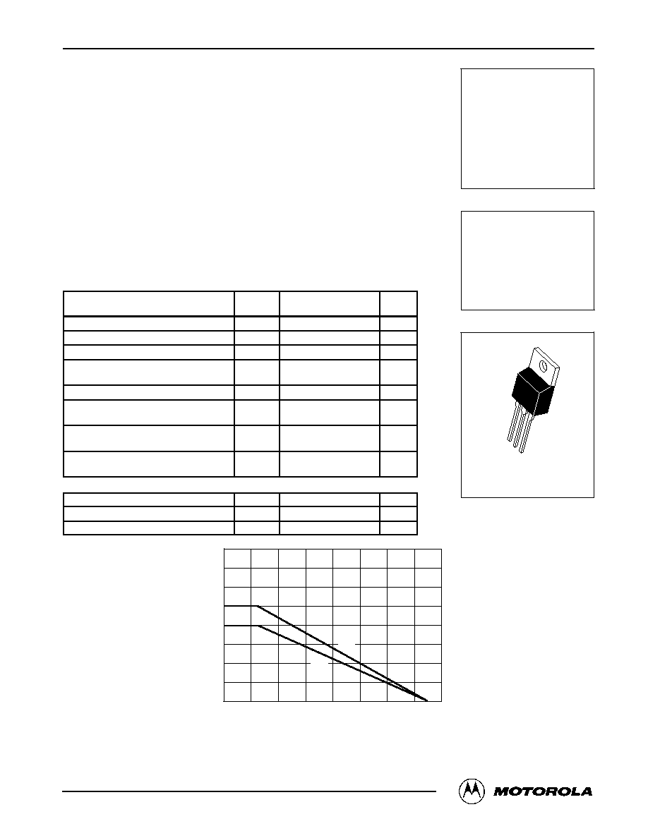
Figure 1. Power Derating
T, TEMPERATURE (
∞
C)
0
40
60
100
120
160
40
TC
20
60
P
D
, POWER DISSIP
A
TION (W
A
TTS)
0
2.0
TA
1.0
3.0
80
140
TC
TA
20
Preferred devices are Motorola recommended choices for future use and best overall value.
MOTOROLA
SEMICONDUCTOR TECHNICAL DATA
Order this document
by MJE15032/D
©
Motorola, Inc. 1997
MJE15032
MJE15033
*Motorola Preferred Device
8.0 AMPERES
POWER TRANSISTORS
COMPLEMENTARY
SILICON
250 VOLTS
50 WATTS
*
NPN
PNP
*
CASE 221A≠06
TO≠220AB

MJE15032 MJE15033
2
Motorola Bipolar Power Transistor Device Data
ŒŒŒŒŒŒŒŒŒŒŒŒŒŒŒŒŒŒŒŒŒŒŒŒŒŒŒŒŒŒŒŒŒŒ
ŒŒŒŒŒŒŒŒŒŒŒŒŒŒŒŒŒŒŒŒŒŒŒŒŒŒŒŒŒŒŒŒŒŒ
ELECTRICAL CHARACTERISTICS
(TC = 25
_
C unless otherwise noted)
ŒŒŒŒŒŒŒŒŒŒŒŒŒŒŒŒŒŒŒŒŒŒŒ
ŒŒŒŒŒŒŒŒŒŒŒŒŒŒŒŒŒŒŒŒŒŒŒ
Characteristic
ŒŒŒŒ
ŒŒŒŒ
Symbol
ŒŒŒŒ
ŒŒŒŒ
Min
ŒŒŒŒ
ŒŒŒŒ
Max
ŒŒŒ
ŒŒŒ
Unit
ŒŒŒŒŒŒŒŒŒŒŒŒŒŒŒŒŒŒŒŒŒŒŒŒŒŒŒŒŒŒŒŒŒŒ
ŒŒŒŒŒŒŒŒŒŒŒŒŒŒŒŒŒŒŒŒŒŒŒŒŒŒŒŒŒŒŒŒŒŒ
OFF CHARACTERISTICS
ŒŒŒŒŒŒŒŒŒŒŒŒŒŒŒŒŒŒŒŒŒŒŒ
Œ
ŒŒŒŒŒŒŒŒŒŒŒŒŒŒŒŒŒŒŒŒŒ
Œ
ŒŒŒŒŒŒŒŒŒŒŒŒŒŒŒŒŒŒŒŒŒŒŒ
Collector≠Emitter Sustaining Voltage (1)
(IC = 10 mAdc, IB = 0)
MJE15032, MJE15033
ŒŒŒŒ
ŒŒŒ
Œ
ŒŒŒŒ
VCEO(sus)
ŒŒŒŒ
Œ
ŒŒ
Œ
ŒŒŒŒ
250
ŒŒŒŒ
Œ
ŒŒ
Œ
ŒŒŒŒ
--
ŒŒŒ
ŒŒ
Œ
ŒŒŒ
Vdc
ŒŒŒŒŒŒŒŒŒŒŒŒŒŒŒŒŒŒŒŒŒŒŒ
Œ
ŒŒŒŒŒŒŒŒŒŒŒŒŒŒŒŒŒŒŒŒŒ
Œ
ŒŒŒŒŒŒŒŒŒŒŒŒŒŒŒŒŒŒŒŒŒŒŒ
Collector Cutoff Current
(VCB = 150 Vdc, IE = 0)
MJE15032, MJE15033
ŒŒŒŒ
ŒŒŒ
Œ
ŒŒŒŒ
ICBO
ŒŒŒŒ
Œ
ŒŒ
Œ
ŒŒŒŒ
--
ŒŒŒŒ
Œ
ŒŒ
Œ
ŒŒŒŒ
10
ŒŒŒ
ŒŒ
Œ
ŒŒŒ
µ
Adc
ŒŒŒŒŒŒŒŒŒŒŒŒŒŒŒŒŒŒŒŒŒŒŒ
ŒŒŒŒŒŒŒŒŒŒŒŒŒŒŒŒŒŒŒŒŒŒŒ
Emitter Cutoff Current
(VBE = 5.0 Vdc, IC = 0)
ŒŒŒŒ
ŒŒŒŒ
IEBO
ŒŒŒŒ
ŒŒŒŒ
--
ŒŒŒŒ
ŒŒŒŒ
10
ŒŒŒ
ŒŒŒ
µ
Adc
ŒŒŒŒŒŒŒŒŒŒŒŒŒŒŒŒŒŒŒŒŒŒŒŒŒŒŒŒŒŒŒŒŒŒ
ŒŒŒŒŒŒŒŒŒŒŒŒŒŒŒŒŒŒŒŒŒŒŒŒŒŒŒŒŒŒŒŒŒŒ
ON CHARACTERISTICS (1)
ŒŒŒŒŒŒŒŒŒŒŒŒŒŒŒŒŒŒŒŒŒŒŒ
Œ
ŒŒŒŒŒŒŒŒŒŒŒŒŒŒŒŒŒŒŒŒŒ
Œ
Œ
ŒŒŒŒŒŒŒŒŒŒŒŒŒŒŒŒŒŒŒŒŒ
Œ
ŒŒŒŒŒŒŒŒŒŒŒŒŒŒŒŒŒŒŒŒŒŒŒ
DC Current Gain
(IC = 0.5 Adc, VCE = 5.0 Vdc)
(IC = 1.0 Adc, VCE = 5.0 Vdc)
(IC = 2.0 Adc, VCE = 5.0 Vdc)
ŒŒŒŒ
ŒŒŒ
Œ
ŒŒŒ
Œ
ŒŒŒŒ
hFE
ŒŒŒŒ
Œ
ŒŒ
Œ
Œ
ŒŒ
Œ
ŒŒŒŒ
50
50
10
ŒŒŒŒ
Œ
ŒŒ
Œ
Œ
ŒŒ
Œ
ŒŒŒŒ
--
--
--
ŒŒŒ
ŒŒ
Œ
ŒŒ
Œ
ŒŒŒ
--
ŒŒŒŒŒŒŒŒŒŒŒŒŒŒŒŒŒŒŒŒŒŒŒ
Œ
ŒŒŒŒŒŒŒŒŒŒŒŒŒŒŒŒŒŒŒŒŒ
Œ
ŒŒŒŒŒŒŒŒŒŒŒŒŒŒŒŒŒŒŒŒŒŒŒ
Collector≠Emitter Saturation Voltage
(IC = 1.0 Adc, IB = 0.1 Adc)
ŒŒŒŒ
ŒŒŒ
Œ
ŒŒŒŒ
VCE(sat)
ŒŒŒŒ
Œ
ŒŒ
Œ
ŒŒŒŒ
--
ŒŒŒŒ
Œ
ŒŒ
Œ
ŒŒŒŒ
0.5
ŒŒŒ
ŒŒ
Œ
ŒŒŒ
Vdc
ŒŒŒŒŒŒŒŒŒŒŒŒŒŒŒŒŒŒŒŒŒŒŒ
Œ
ŒŒŒŒŒŒŒŒŒŒŒŒŒŒŒŒŒŒŒŒŒ
Œ
ŒŒŒŒŒŒŒŒŒŒŒŒŒŒŒŒŒŒŒŒŒŒŒ
Base≠Emitter On Voltage
(IC = 1.0 Adc, VCE = 5.0 Vdc)
ŒŒŒŒ
ŒŒŒ
Œ
ŒŒŒŒ
VBE(on)
ŒŒŒŒ
Œ
ŒŒ
Œ
ŒŒŒŒ
--
ŒŒŒŒ
Œ
ŒŒ
Œ
ŒŒŒŒ
1.0
ŒŒŒ
ŒŒ
Œ
ŒŒŒ
Vdc
ŒŒŒŒŒŒŒŒŒŒŒŒŒŒŒŒŒŒŒŒŒŒŒŒŒŒŒŒŒŒŒŒŒŒ
ŒŒŒŒŒŒŒŒŒŒŒŒŒŒŒŒŒŒŒŒŒŒŒŒŒŒŒŒŒŒŒŒŒŒ
DYNAMIC CHARACTERISTICS
ŒŒŒŒŒŒŒŒŒŒŒŒŒŒŒŒŒŒŒŒŒŒŒ
ŒŒŒŒŒŒŒŒŒŒŒŒŒŒŒŒŒŒŒŒŒŒŒ
Current Gain -- Bandwidth Product (2)
(IC = 500 mAdc, VCE = 10 Vdc, ftest = 1.0 MHz)
ŒŒŒŒ
ŒŒŒŒ
fT
ŒŒŒŒ
ŒŒŒŒ
30
ŒŒŒŒ
ŒŒŒŒ
--
ŒŒŒ
ŒŒŒ
MHz
(1) Pulse Test: Pulse Width
v
300
µ
s, Duty Cycle
v
2.0%.
(2) fT =
hfe
∑
ftest.
t, TIME (ms)
0.01
0.01
0.05
1.0
2.0
5.0
10
20
50
500
1.0 k
0.1
0.5
0.2
1.0
0.2
0.1
0.05
r(t)
, TRANSIENT
THERMAL
Z
JC(t) = r(t) R
JC
R
JC = 1.56
∞
C/W MAX
D CURVES APPLY FOR POWER
PULSE TRAIN SHOWN
READ TIME AT t1
TJ(pk) ≠ TC = P(pk) Z
JC(t)
P(pk)
t1
t2
DUTY CYCLE, D = t1/t2
0.2
SINGLE PULSE
RESIST
ANCE (NORMALIZED)
Figure 2. Thermal Response
0.5
D = 0.5
0.05
0.3
0.7
0.07
0.03
0.02
0.02
100
200
0.1
0.02
0.01

MJE15032 MJE15033
3
Motorola Bipolar Power Transistor Device Data
250 ms
100
µ
s
50 ms
10 ms
100
1.0
Figure 3. MJE15032 & MJE15033
Safe Operating Area
VCE, COLLECTOR≠EMITTER VOLTAGE (VOLTS)
10
0.01
I C
, COLLECT
OR
CURRENT
(AMPS)
10
1000
1.0
100
0.1
There are two limitations on the power handling ability of a
transistor: average junction temperature and second break-
down. Safe operating area curves indicate IC ≠ VCE limits of
the transistor that must be observed for reliable operation,
i.e., the transistor must not be subjected to greater dissipa-
tion then the curves indicate.
The data of Figures 3 and 4 is based on TJ(pk) = 150
_
C;
TC is variable depending on conditions. Second breakdown
pulse limits are valid for duty cycles to 10% provided TJ(pk)
< 150
_
C. TJ(pk) may be calculated from the data in Figure 2.
At high case temperatures, thermal limitations will reduce the
power that can be handled to values less than the limitations
imposed by second breakdown.
25
∞
C
150
∞
C
≠55
∞
C
1000
0.1
Figure 4. NPN -- MJE15032
VCE = 5 V DC Current Gain
IC, COLLECTOR CURRENT (AMPS)
1.0
h
FE
, DC CURRENT
GAIN
10
100
10
1.0
Figure 5. PNP -- MJE15033
VCE = 5 V DC Current Gain
Figure 6. NPN -- MJE15032
VCE = 5 V VBE(on) Curve
IC, COLLECTOR CURRENT (AMPS)
1.0
10
1.0
10
V
,
VOL
T
AGE
(VOL
TS)
0.1
0.1
Figure 7. PNP -- MJE15033
VCE = 5 V VBE(on) Curve
IC, COLLECTOR CURRENT (AMPS)
10
V
,
VOL
T
AGE
(VOL
TS)
1.0
10
0.1
0.1
1.0
NPN -- MJE15032
PNP -- MJE15033
25
∞
C
150
∞
C
≠55
∞
C
25
∞
C
150
∞
C
≠55
∞
C
1000
0.1
IC, COLLECTOR CURRENT (AMPS)
1.0
h
FE
, DC CURRENT
GAIN
10
100
10
1.0
25
∞
C
150
∞
C
≠55
∞
C

MJE15032 MJE15033
4
Motorola Bipolar Power Transistor Device Data
IC, COLLECTOR CURRENT (AMPS)
IC, COLLECTOR CURRENT (AMPS)
V
,
VOL
T
AGE
(VOL
TS)
Figure 8. NPN -- MJE15032
VCE(sat) IC/IB = 10
Figure 9. PNP -- MJE15033
VCE(sat) IC/IB = 10
1.0
10
10
0.1
0.1
0.01
1.0
0.1
IC, COLLECTOR CURRENT (AMPS)
100
10
1.0
0.1
0.01
V
,
VOL
T
AGE
(VOL
TS)
NPN -- MJE15032
PNP -- MJE15033
100
1.0
0.1
0.01
V
,
VOL
T
AGE
(VOL
TS)
V
,
VOL
T
AGE
(VOL
TS)
Figure 10. NPN -- MJE15032
VCE(sat) IC/IB = 20
Figure 11. PNP -- MJE15033
VCE(sat) IC/IB = 20
10
0.1
1.0
10
1.0
0.1
IC, COLLECTOR CURRENT (AMPS)
10
1.0
0.1
V
Figure 12. NPN -- MJE15032
VBE(sat) IC/IB = 10
Figure 13. PNP -- MJE15033
VBE(sat) IC/IB = 10
10
1.0
10
25
∞
C
150
∞
C
≠55
∞
C
25
∞
C
150
∞
C
≠55
∞
C
25
∞
C
150
∞
C
≠55
∞
C
IC, COLLECTOR CURRENT (AMPS)
100
1.0
0.1
0.01
10
0.1
1.0
10
25
∞
C
150
∞
C
≠55
∞
C
, BASE EMITTER VOL
T
AGE
(VOL
TS)
BE
0.1
IC, COLLECTOR CURRENT (AMPS)
10
1.0
0.1
V
10
1.0
, BASE EMITTER VOL
T
AGE
(VOL
TS)
BE
25
∞
C
150
∞
C
≠55
∞
C
25
∞
C
150
∞
C
≠55
∞
C

MJE15032 MJE15033
5
Motorola Bipolar Power Transistor Device Data
PACKAGE DIMENSIONS
CASE 221A≠06
TO≠220AB
ISSUE Y
NOTES:
1. DIMENSIONING AND TOLERANCING PER ANSI
Y14.5M, 1982.
2. CONTROLLING DIMENSION: INCH.
3. DIMENSION Z DEFINES A ZONE WHERE ALL
BODY AND LEAD IRREGULARITIES ARE
ALLOWED.
STYLE 1:
PIN 1. BASE
2. COLLECTOR
3. EMITTER
4. COLLECTOR
DIM
MIN
MAX
MIN
MAX
MILLIMETERS
INCHES
A
0.570
0.620
14.48
15.75
B
0.380
0.405
9.66
10.28
C
0.160
0.190
4.07
4.82
D
0.025
0.035
0.64
0.88
F
0.142
0.147
3.61
3.73
G
0.095
0.105
2.42
2.66
H
0.110
0.155
2.80
3.93
J
0.018
0.025
0.46
0.64
K
0.500
0.562
12.70
14.27
L
0.045
0.060
1.15
1.52
N
0.190
0.210
4.83
5.33
Q
0.100
0.120
2.54
3.04
R
0.080
0.110
2.04
2.79
S
0.045
0.055
1.15
1.39
T
0.235
0.255
5.97
6.47
U
0.000
0.050
0.00
1.27
V
0.045
≠≠≠
1.15
≠≠≠
Z
≠≠≠
0.080
≠≠≠
2.04
B
Q
H
Z
L
V
G
N
A
K
F
1
2 3
4
D
SEATING
PLANE
≠T≠
C
S
T
U
R
J