 | ÐлекÑÑоннÑй компоненÑ: TDA1085CD | СкаÑаÑÑ:  PDF PDF  ZIP ZIP |
Äîêóìåíòàöèÿ è îïèñàíèÿ www.docs.chipfind.ru
Device
Operating
Temperature Range
Package
TDA1085C
SEMICONDUCTOR
TECHNICAL DATA
UNIVERSAL MOTOR
SPEED CONTROLLER
ORDERING INFORMATION
TDA1085CD
TDA1085C
TJ = 10
°
to +120
°
C
SO16
Plastic DIP
Order this document by TDA1085C/D
PLASTIC PACKAGE
CASE 648
D SUFFIX
PLASTIC PACKAGE
CASE 751B
(SO16)
16
1
16
1
1
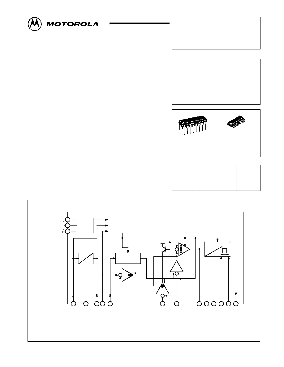
MOTOROLA ANALOG IC DEVICE DATA
Universal Motor
Speed Controller
The TDA1085C is a phase angle triac controller having all the necessary
functions for universal motor speed control in washing machines. It operates
in closed loop configuration and provides two ramp possibilities.
·
OnChip Frequency to Voltage Converter
·
OnChip Ramps Generator
·
SoftStart
·
Load Current Limitation
·
Tachogenerator Circuit Sensing
·
Direct Supply from AC Line
·
Security Functions Peformed by Monitor
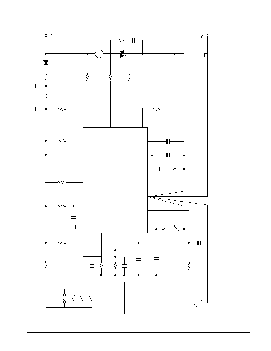
Figure 1. Representative Block Diagram and Pin Connections
Reset
Control
Amp.
=
VCC
Current
Limiter
0.7 V
+
Ramp
Generator
Speed
Detector
Shunt Regulator
Ballast Resistor
+ VCC
Monitoring
Voltage
Reg
Digital Speed Sense
F/VC Pump Capacitor
Actual Speed
Set Speed
Ramp Current Gen. Control
Motor Current Limit
Ramp Gen.
T
iming
Closed Loop Stability
Sawtooth Capacitor
Sawtooth Set Current
V
oltage Synchronization
Current Synchronization
T
rigger Pulse Output
Trigger Pulse
Gen.
9
10
8
12
11
4
5
6
3
7
16
14
15
2
1
13
©
Motorola, Inc. 1996
Rev 5
TDA1085C
2
MOTOROLA ANALOG IC DEVICE DATA
MAXIMUM RATINGS
(TA = 25
°
C, voltages are referenced to Pin 8, ground)
Rating
Symbol
Value
Unit
Power Supply, when externally regulated, VPin 9
VCC
15
V
Maximum Voltage per listed pin
Pin 3
Pin 4567131416
Pin 10
VPin
+ 5.0
0 to + VCC
0 to + 17
V
Maximum Current per listed pin
Pin 1 and 2
Pin 3
Pin 9 (VCC)
Pin 10 shunt regulator
Pin 12
Pin 13
IPin
3.0 to + 3.0
1.0 to + 0
15
35
1.0 to + 1.0
200
mA
Maximum Power Dissipation
PD
1.0
W
Thermal Resistance, JunctiontoAir
R
JA
65
°
C/W
Operating Junction Temperature
TJ
10 to + 120
°
C
Storage Temperature Range
Tstg
55 to + 150
°
C
ELECTRICAL CHARACTERISTICS
(TA = 25
°
C)
Characteristic
Symbol
Min
Typ
Max
Unit
VOLTAGE REGULATOR
Internally Regulated Voltage (VPin 9)
(IPin 7 = 0, IPin 9 + IPin 10 = 15 mA, IPin 13 = 0)
VCC
15
15.3
15.6
V
VCC Temperature Factor
TF
--
100
--
ppm/
°
C
Current Consumption (IPin 9)
(V9 = 15 V, V12 = V8 = 0, I1 = I2 = 100
µ
A,
all other pins not connected)
ICC
--
4.5
6.0
mA
VCC Monitoring Enable Level
VCC Monitoring
Disable Level
VCC EN
VCC DIS
--
--
VCC 0.4
VCC 1.0
--
--
V
RAMP GENERATOR
Reference Speed Input Voltage Range
VPin 5
0.08
--
13.5
V
Reference Input Bias Current
IPin 5
0
0.8
1.0
µ
A
Ramp Selection Input Bias Current
IPin 6
0
--
1.0
µ
A
Distribution Starting Level Range
VDS
0
--
2.0
V
Distribution Final Level
VPin 6 = 0.75 V
VDF/VDS
2.0
2.09
2.2
High Acceleration Charging Current
VPin 7 = 0 V
VPin 7 = 10 V
IPin 7
1.0
1.0
--
1.2
1.7
1.4
mA
Distribution Charging Current
VPin 7 = 2.0 V
IPin 7
4.0
5.0
6.0
µ
A
TDA1085C
3
MOTOROLA ANALOG IC DEVICE DATA
ELECTRICAL CHARACTERISTICS
(continued)
Characteristic
Symbol
Min
Typ
Max
Unit
CURRENT LIMITER
Limiter Current Gain -- IPin 7/IPin 3
(IPin3 = 300
µ
A)
Cg
130
180
250
Detection Threshold Voltage
IPin 3 = 10
µ
A
VPin 3 TH
50
65
80
mV
FREQUENCY TO VOLTAGE CONVERTER
Input Signal "Low Voltage"
Input Signal "High Voltage"
Monitoring Reset Voltage
V12 L
V12 H
V12 R
100
+100
5.0
--
--
--
--
--
--
mV
mV
V
Negative Clamping Voltage
IPin 12 = 200
µ
A
V12 CL
--
0.6
--
V
Input Bias Current
IPin12
--
25
--
µ
A
Internal Current Source Gain
G
+
I
Pin 4
I
Pin 11
, V
Pin 4
+
V
Pin 11
+
0
G.0
9.5
--
11
Gain Linearity versus Voltage on Pin 4
(G8.6 = Gain for VPin 4 = 8.6 V)
V4 = 0 V
V4 = 4.3 V
V4 = 12 V
G/G8.6
1.04
1.015
0.965
1.05
1.025
0.975
1.06
1.035
0.985
Gain Temperature Effect (VPin 4 = 0)
TF
--
350
--
ppm/
°
C
Output Leakage Current (IPin 11 = 0)
IPin 4
0
--
100
nA
CONTROL AMPLIFIER
Actual Speed Input Voltage Range
VPin 4
0
--
13.5
V
Input Offset Voltage VPin 5 VPin 4
(IPin 16 = 0, VPin 16 = 3.0 and 8.0 V)
Voff
0
--
50
mV
Amplifier Transconductance
(IPin 16/
(V5 V4)
(IPin 16 = + and 50
µ
A, VPin 16 = 3.0 V)
T
270
340
400
µ
A/V
Output Current Swing Capability
Source
Sink
IPin 16
200
50
100
100
50
200
µ
A
Output Saturation Voltage
V16 sat
--
--
0.8
V
TRIGGER PULSE GENERATOR
Synchronization Level Currents
Voltage Line Sensing
Triac Sensing
IPin 2
IPin 1
--
--
±
50
±
50
±
100
±
100
µ
A
Trigger Pulse Duration (CPin 14 = 47 nF, RPin 15 = 270 k
)
Tp
--
55
--
µ
s
Trigger Pulse Repetition Period, conditions as a.m.
TR
--
220
--
µ
s
Output Pulse Current VPin 13 = VCC 4.0 V
IPin 13
180
192
--
mA
Output Leakage Current VPin 13 = 3.0 V
I13 L
--
--
30
µ
A
Full Angle Conduction Input Voltage
V14
--
11.7
--
V
Saw Tooth "High" Level Voltage
V14 H
12
--
12.7
V
Saw Tooth Discharge Current, IPin15 = 100
µ
A
IPin 14
95
--
105
µ
A

TDA1085C
4
MOTOROLA ANALOG IC DEVICE DATA
GENERAL DESCRIPTION
The TDA 1085C triggers a triac accordingly to the speed regulation
requirements. Motor speed is digitally sensed by a tachogenerator
and then converted into an analog voltage.
The speed set is externally fixed and is applied to the internal linear
regulation input after having been submitted to programmable
acceleration ramps. The overall result consists in a full motor speed
range with two acceleration ramps which allow efficient washing
machine control (Distribute function).
Additionally, the TDA 1085C protects the whole system against AC
line stop or variations, overcurrent in the motor and tachogenerator
failure.
INPUT/OUTPUT FUNCTIONS
(Refer to Figures 1 and 8)
Voltage Regulator (Pins 9 and 10) This is a parallel type regulator
able to sink a large amount of current and offering good
characteristics. Current flow is provided from AC line by external
dropping resistors R1, R2, and rectifier: This half wave current is
used to feed a smoothering capacitor, the voltage of which is
checked by the IC.
When VCC is reached, the excess of current is derived by another
dropping resistor R10 and by Pin 10. These three resistors must be
determined in order:
·
To let 1.0 mA flow through Pin 10 when AC line is minimum and VCC
consumption is maximum (fast ramps and pulses present).
·
To let V10 reach 3.0 V when AC line provides maximum current and
VCC consumption is minimum (no ramps and no pulses).
·
All along the main line cycle, the Pin 10 dynamic range must not be
exceeded unless loss of regulation.
An AC line supply failure would cause shut down.
The double capacitive filter built with R1 and R2 gives an efficient
VCC smoothing and helps to remove noise from set speeds.
Speed Sensing (Pins 4, 11, 12) The IC is compatible with an
external analog speed sensing: its output must be applied to Pin 4,
and Pin 12 connected to Pin 8.
In most of the applications it is more convenient to use a digital
speed sensing with an unexpensive tachogenerator which
doesn
t need any tuning. During every positive cycle at Pin 12,
the capacitor CPin 11 is charged to almost VCC and during this
time, Pin 4 delivers a current which is 10 times the one charging
CPin 11. The current source gain is called G and is tightly
specified, but nevertheless requires an adjustment on RPin 4. The
current into this resistor is proportional to CPin 11 and to the motor
speed; being filtered by a capacitor, VPin 4 becomes smothered
and represents the "true actual motor speed".
To maintain linearity into the high speed range, it is important to verify
that CPin 11 is fully charged: the internal source on Pin 11 has 100 K
impedance. Nevertheless CPin 11 has to be as high as possible as it
has a large influence on FV/C temperature factor. A 470 K
resistor
between Pins 11 and 9 reduces leakage currents and temperature
factor as well, down to neglectable effects.
Pin 12 also has a monitoring function: when its voltage is above
5.0 V, the trigger pulses are inhibited and the IC is reset. It also
senses the tachogenerator continuity, and in case of any circuit
aperture, it inhibits pulse, avoiding the motor to run out of control. In
the TDA 1085C, Pin 12 is negatively clamped by an internal diode
which removes the necessity of the external one used in the former
circuit.
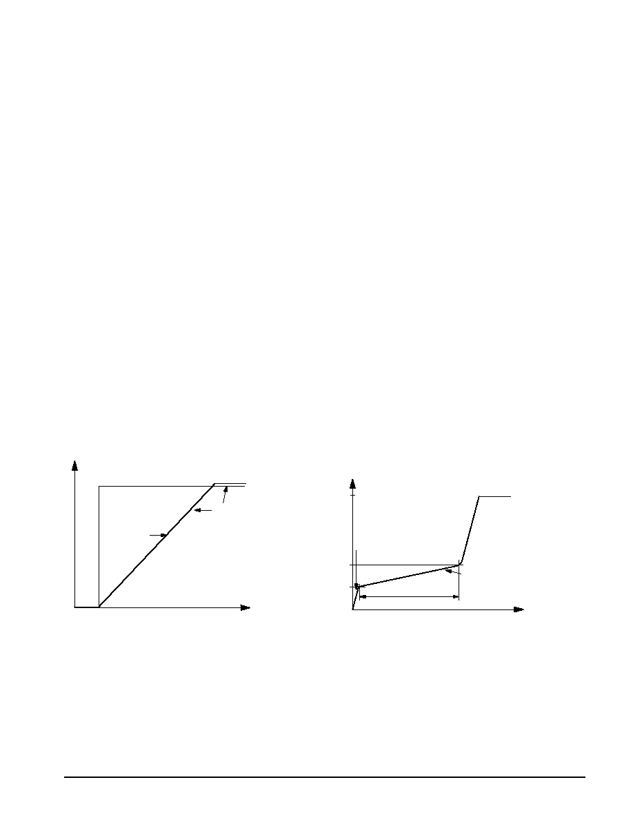
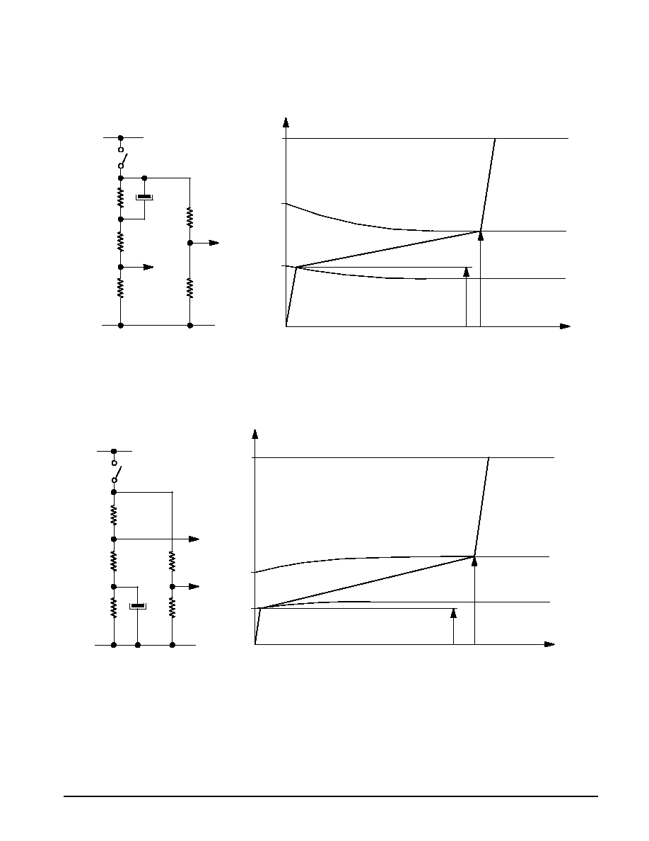
Ramp Generator (Pins 5, 6, 7) The true Set Speed value taken in
consideration by the regulation is the output of the ramp generator
(Pin 7). With a given value of speed set input (Pin 5), the ramp
generator charges an external capacitor CPin 7 up to the moment
VPin 5 (set speed) equals VPin 4 (true speed), see Figure 2. The IC
has an internal charging current source of 1.2mA and delivers it from
0 to 12 V at Pin 7. It is the high acceleration ramp (5.0 s typical) which
allows rapid motor speed changes without excessive strains on the
mechanics. In addition, the TDA 1085C offers the possibility to break
this high acceleration with the introduction of a low acceleration ramp
(called Distribution) by reducing the Pin 7 source current down to
5.0
µ
A under Pin 6 full control, as shown by following conditions:
·
Presence of high acceleration ramp VPin 5 > VPin 4
·
Distribution occurs in the VPin 4 range (true motor speed) defined
by VPin 6
x
VPin 4
x
2.0 VPin 6
For two fixed values of VPin 5 and VPin 6, the motor speed will have
high acceleration, excluding the time for VPin 4 to go from VPin 6
to two times this value, high acceleration again, up to the moment
the motor has reached the set speed value, at which it will stay,
see Figure 3.
Should a reset happen (whatever the cause would be), the above
mentioned successive ramps will be fully reprocessed from 0 to the
maximum speed. If VPin 6 = 0, only the high acceleration ramp
occurs.
To get a real zero speed position, Pin 5 has been designed in such a
way that its voltage from 0 to 80 mV is interpreted as a true zero. As
a consequence, when changing the speed set position, the designer
must be sure that any transient zero would not occur: if any, the entire
circuit will be reset.
As the voltages applied by Pins 5 and 6 are derived from the internal
voltage regulator supply and Pin 4 voltage is also derived from the
same source, motor speed (which is determined by the ratios
between above mentioned voltages) is totally independent from VCC
variations and temperature factor.
Control Amplifier (Pin 16) It amplifies the difference between true
speed (Pin 4) and set speed (Pin 5), through the ramp generator. Its
output available at Pin 16 is a double sense current source with a
maximum capability of
±
100
µ
A and a specified transconductance
(340
µ
A/V typical). Pin 16 drives directly the trigger pulse generator,
and must be loaded by an electrical network which compensates the
mechanical characteristics of the motor and its load, in order to
provide stability in any condition and shortest transient response; see
Figure 4.
This network must be adjusted experimentally.
In case of a periodic torque variations, Pin 16 directly provides the
phase angle oscillations.

TDA1085C
5
MOTOROLA ANALOG IC DEVICE DATA
Trigger Pulse Generator (Pins 1, 2, 5, 13, 14, 15)
This circuit performs four functions:
·
The conversion of the control amplifier DC output level to a
proportional firing angle at every main line half cycle.
·
The calibration of pulse duration.
·
The repetition of the pulse if the triac fails to latch on if the current
has been interrupted by brush bounce.
·
The delay of firing pulse until the current crosses zero at wide firing
angles and inductive loads.
RPin 15 programs the Pin 14 discharging current. Saw tooth signal is
then fully determined by R15 and C14 (usually 47 nF). Firing pulse
duration and repetition period are in inverse ratio to the saw tooth
slope.
Pin 13 is the pulse output and an external limiting resistor is
mandatory. Maximum current capability is 200 mA.
Current Limiter (Pin 3) Safe operation of the motor and triac under
all conditions is ensured by limiting the peak current. The motor
current develops an alternative voltage in the shunt resistor (0.05
in Figure 4). The negative half waves are transferred to Pin 3 which
is positively preset at a voltage determined by resistors R3 and R4.
As motor current increases, the dynamical voltage range of Pin 3
increases and when Pin 3 becomes slightly negative in respect to
Pin 8, a current starts to circulate in it. This current, amplified
typically 180 times, is then used to discharge Pin 7 capacitor and, as
a result, reduces firing angle down to a value where an equilibrium is
reached. The choice of resistors R3, R4 and shunt determines the
magnitude of the discharge current signals on CPin 7.
Notice that the current limiter acts only on peak triac current.
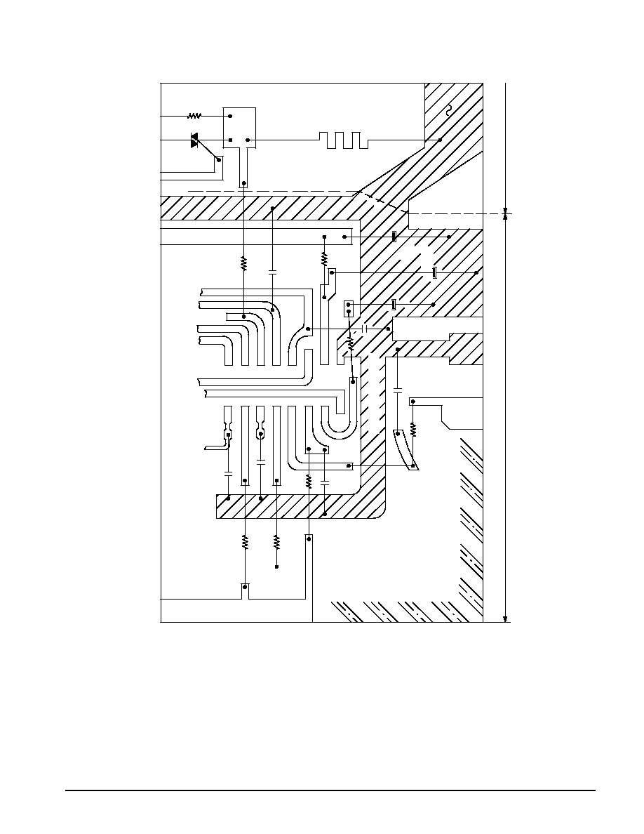
APPLICATION NOTES
(Refer to Figure 4)
Printed Circuit Layout Rules
In the common applications, where TDA 1085C is used, there is on
the same board, presence of high voltage, high currents as well as
low voltage signals where millivolts count. It is of first magnitude
importance to separate them from each other and to respect the
following rules:
·
Capacitor decoupling pins, which are the inputs of the same
comparator, must be physically close to the IC, close to each other
and grounded in the same point.
·
Ground connection for tachogenerator must be directly connected
to Pin 8 and should ground only the tacho. In effect, the latter is a
first magnitude noise generator due to its proximity to the motor
which induces high d
/dt signals.
·
The ground pattern must be in the "star style" in order to fully
eliminate power currents flowing in the ground network devoted to
capacitors decoupling sensitive Pins: 4, 5, 7, 11, 12, 14, 16.
As an example, Figure 5 presents a PC board pattern which
concerns the group of sensitive Pins and their associated capacitors
into which the a.m. rules have been implemented. Notice the full
separation of "Signal World" from "Power", one by line AB and their
communication by a unique strip.
These rules will lead to much satisfactory volume production in the
sense that speed adjustment will stay valid in the entire speed
range.
Power Supply
As dropping resistor dissipates noticeable power, it is necessary to
reduce the ICC needs down to a minimum. Triggering pulses, if a
certain number of repetitions are kept in reserve to cope with motor
brush wearing at the end of its life, are the largest ICC user. Classical
worst case configuration has to be considered to select dropping
resistor. In addition, the parallel regulator must be always into its
dynamic range, i.e., IPin 10 over 1.0 mA and VPin 10 over 3.0 V in any
extreme configuration. The double filtering cell is mandatory.
Tachogenerator Circuit
The tacho signal voltage is proportional to the motor speed. Stablility
considerations, in addition, require an RC filter, the pole of which
must be looked at. The combination of both elements yield a constant
amplitude signal on Pin 12 in most of the speed range. It is
recommended to verify this maximum amplitude to be within 1.0 V
peak in order to have the largest signal/noise ratio without resetting
the integrated circuit (which occurs if VPin 12 reaches 5.5 V). It must
be also verified that the Pin 12 signal is approximately balanced
between "high" (over 300 mV) and "low". An 8poles tacho is a
minimum for low speed stability and a 16poles is even better.
The RC pole of the tacho circuit should be chosen within 30 Hz in
order to be as far as possible from the 150 Hz which corresponds to
the AC line 3rd harmonic generated by the motor during starting
procedure. In addition, a high value resistor coming from VCC
introduces a positive offset at Pin 12, removes noise to be interpreted
as a tacho signal. This offset should be designed in order to let Pin 12
reach at least 200 mV (negative voltage) at the lowest motor speed.
We remember the necessity of an individual tacho ground
connection.
Frequency to Voltage Converter F V/C
CPin 11 has a recommended value of 820 pF for 8poles tachos and
maximum motor rpm of 15000, and RPin 11 must be always 470 K.
RPin 4 should be choosen to deliver within 12 V at maximum motor
speed in order to maximize signal/noise ratio. As the FV/C ratio as
well as the CPin 11 value are dispersed, RPin 4 must be adjustable and
should be made of a fixed resistor in serice with a trimmer
representing 25% of the total. Adjustment would become easier.
Once adjusted, for instance at maximum motor speed, the FV/C
presents a residual non linearity; the conversion factor (mV per RPM)
increases by within 7.7% as speed draws to zero. The guaranteed
dispersion of the latter being very narrow, a maximum 1% speed
error is guaranteed if during Pin 5 network design the small set
values are modified, once forever, according this increase.
The following formulas give VPin 4:
V
Pin 4
+
G.0
@
(V
CC
Va)
@
C
Pin 11
@
R
4
@
f
@
(1
)
120k
R
Pin11
)
1
In volts.
G.0 . (VCC Va)
'
140
Va = 2.0 VBE
120 k = Rint, on Pin 11
Speed Set
(Pin 5) Upon designer choice, a set of external
resistors apply a series of various voltages corresponding to the
various motor speeds. When switching external resistors, verify that
no voltage below 80 mV is ever applied to Pin 5. If so, a full circuit
reset will occur.
TDA1085C
6
MOTOROLA ANALOG IC DEVICE DATA
Ramps Generator (Pin 6) If only a high acceleration ramp is
needed, connect Pin 6 to ground.
When a Distribute ramp should occur, preset a voltage on Pin 6
which corresponds to the motor speed starting ramp point.
Distribution (or low ramp) will continue up to the moment the motor
speed would have reached twice the starting value.
The ratio of two is imposed by the IC. Nevertheless, it could be
externally changed downwards (Figure 6) or upwards (Figure 7).
The distribution ramp can be shortened by an external resistor from
VCC charging CPin 7, adding its current to the internal 5.0
µ
A
generator.
Power Circuits
Triac Triggering pulse amplitude must be determined by Pin 13
resistor according to the needs in Quadrant IV. Trigger pulse duration
can be disturbed by noise signals generated by the triac itself, which
interfere within Pins 14 and 16, precisely those which determine it.
While easily visible, this effect is harmless.
The triac must be protected from high AC line dV/dt during external
disturbances by 100 nF x 100
network.
Shunt resistor must be as noninductive as possible. It can be made
locally by using constantan alloy wire.
When the load is a DC fed universal motor through a rectifier bridge,
the triac must be protected from commutating dV/dt by a 1.0 to
2.0 mH coil in series with MT2.
Synchronization functions are performed by resistors sensing AC
line and triac conduction. 820 k values are normal but could be
reduced down to 330 k in order to detect the "zeros" with accuracy
and to reduce the residual DC line component below 20 mA.
Current Limitation
The current limiter starts to discharge Pin 7 capacitor (reference
speed) as the motor current reaches the designed threshold level.
The loop gain is determined by the resistor connecting Pin 3 to the
series shunt. Experience has shown that its optimal value for a
10 Arms limitation is within 2.0 k
. Pin 3 input has a sensitivity in
current which is limited to reasonable values and should not react to
spikes.
If not used, Pin 3 must be connected to a maximum positive voltage
of 5.0 V rather than be left open.
Loop Stability
The Pin 16 network is predominant and must be adjusted
experimentally during module development. The values indicated in
Figure 4 are typical for washing machine applications but accept
large modifications from one model to another. R16 (the sole
restriction) should not go below 33 k, otherwise slew rate limitation
will cause large transient errors for load steps.
Figure 2. Acceleration Ramp
Figure 3. Programmable Double
Acceleration Ramp
V
VPin 5
VPin 7
t
0
VPin 6 = VDS
0
VDS
VDF
High Acceleration
Ramp
Distribution
Low Acceleration
Ramp
High Acceleration
Ramp
VPin 5 fixed set value
Speeds
t
VPin 4
VDF = 2 VDS
TDA1085C
7
MOTOROLA ANALOG IC DEVICE DATA
680
R7
1500
k
R1
1
470
k
R15
R10
R4
270
6.8
k
1N4007
R1
820
k
R2
820
k
120
100
100n
Shunt
50 m
R3
2.7
k
C14
47n
C16
100n
47
µ
R16
68
k
150
k
50
k
220n
22
k
1.0
µ
470
µ
C7
1.0
µ
68
k
47
k
1.0
µ
Ramp
Speed
Speed/Ramp
Selector
Resistive
Network
T
acho Generator
Figure 4. Basic Application Circuit
Current limitation: 10
A
adjusted by R4 experimentally
Ramps High acceleration: 3200 rpm per second
Distribution ramp: 10 s from 850 to 1300 rpm
Speeds:
W
ash 800 rpm
Distribution 1300
Spin 1: 7500
Spin 2: 15,000
Pin 5 V
oltage
Set:
609 mV
996 mV
5,912 V
12,000 V
Including nonlinearity corrections
Including nonlinearity corrections
Including nonlinearity corrections
Adjustment point
Motor Speed Range: 0 to 15,000 rpm
T
achogenerator 8 poles delivering 30 V peak to peak at 6000 rpm, in open circuit
FV/C Factor: 8 mV per rpm (12 V full speed) C
Pin
1
1
= 680 pF
V
CC
= 15.3 V
T
riac
MAX15A8
15 A
600
V
Igt min = 90 mA
to cover Quad IV at 10
°
C
1
1
15
9
1
0
2
1
13
3
14
16
8
12
4
5
6
7
TDA1085C
+V
CC
C1
1
820 pF
100
µ
100
µ
M
TDA1085C
8
MOTOROLA ANALOG IC DEVICE DATA
Figure 5. PC Board Layout
270
k
120
100
nF
47
nF
470
k
820
pF
16
15
14
13
12
11
10
9
1
2
3
4
5
6
7
8
1.0
µ
F
V CC
A
B
MT2
MT1
470
µ
F
+VCC
V
CC
0.22
µ
F
Ground Connection
TDA1085C
9
MOTOROLA ANALOG IC DEVICE DATA
Pin 6
VCC
C
R3
R2
R1
R5
R4
Distribute
and Spin 1
Contact
V
2VPin 6t
VPin 6t
t
k < 2
Spin 1 (defined by R5/R4 + R5)
0
0
VPin 6
For k = 1.6, R3 = 0.6 (R1 + R2),
R3 C within 4 seconds
2VPin 6
Pin 5
Figure 6. Distribution Speed k < 2
SD + S1
VCC
Pin 6
k > 2
t
2VPin 6t
VPin 6t
Spin 1
V
VPin 6
2VPin 6
Pin 5
0
0
Figure 7. Distribution Speed k > 2
TDA1085C
10
MOTOROLA ANALOG IC DEVICE DATA
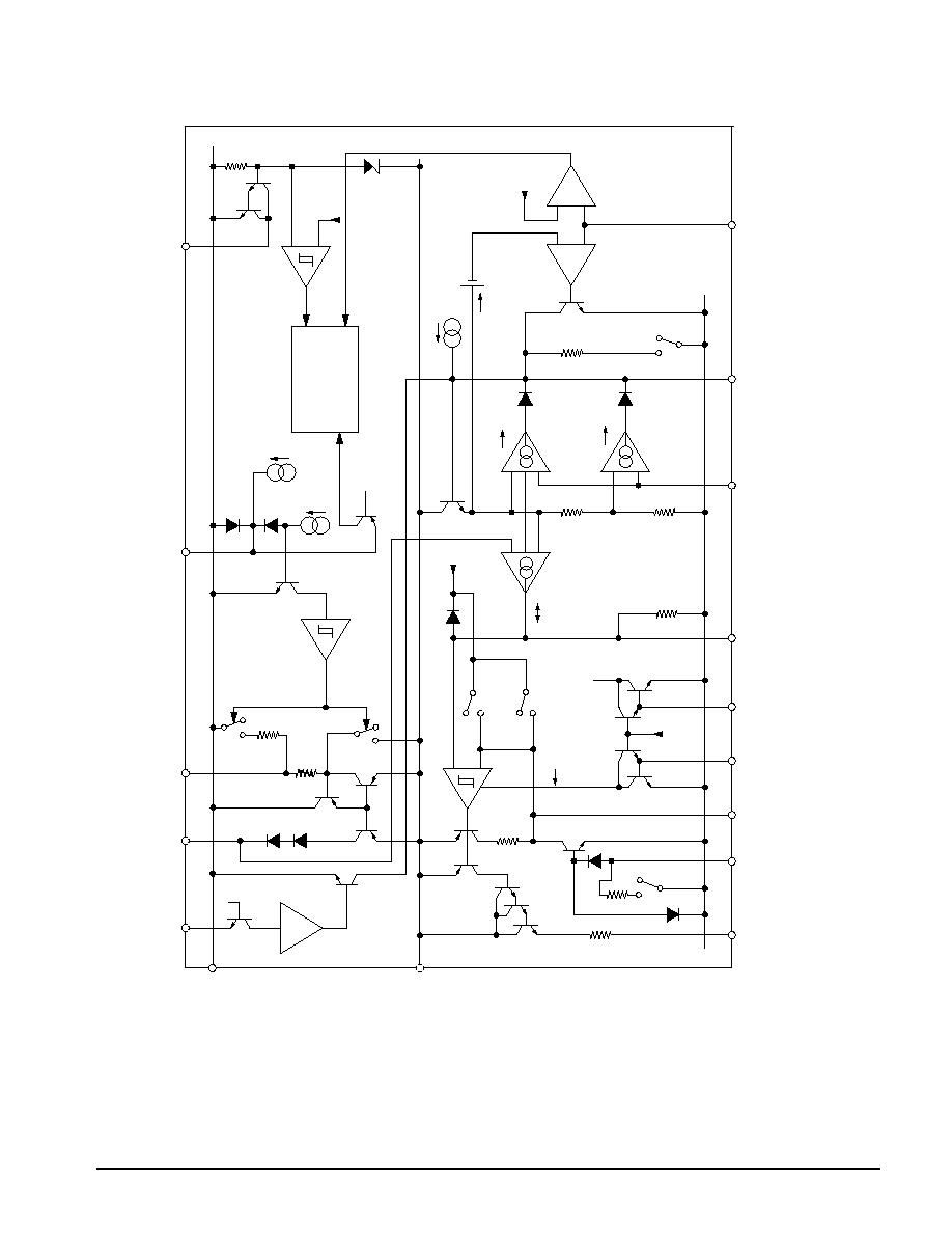
Figure 8. Simplified Schematic
3
4
1
1
12
10
8
9
13
15
14
1
2
16
6
7
5
0.7
V
I
6
I
7
I
2
I
1
0.7
V
"ON"
for Ip2 = 0
Enable
for Ip1 # 0
R1=R2
R1
R2
V
CC
1.2
mA
1.2
mA
5.7
V
25
µ
A
5.0
µ
A
0.6
V
5.0
µ
A
+V
CC
80
mV
I
5
+
+
+
MONIT
ORING
IF*
*(P12 connected) and (V
CC
OK) and (VP5>80
mV)
Then
I
1 OFF),
(
I
2 OFF),
(
I
4 OFF) and
(
I
5 OFF)
(
I
3
V
CC
0.7 V
TDA1085C
11
MOTOROLA ANALOG IC DEVICE DATA
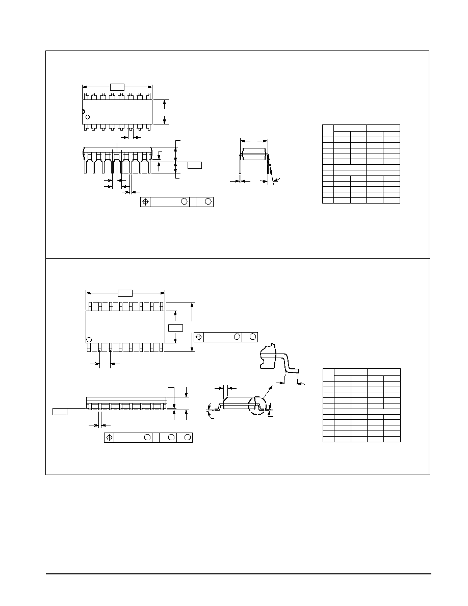
PLASTIC PACKAGE
CASE 64808
ISSUE R
D SUFFIX
PLASTIC PACKAGE
CASE 751B05
ISSUE J
(SO16)
OUTLINE DIMENSIONS
NOTES:
1. DIMENSIONING AND TOLERANCING PER ANSI
Y14.5M, 1982.
2. CONTROLLING DIMENSION: INCH.
3. DIMENSION L TO CENTER OF LEADS WHEN
FORMED PARALLEL.
4. DIMENSION B DOES NOT INCLUDE MOLD FLASH.
5. ROUNDED CORNERS OPTIONAL.
A
B
F
C
S
H
G
D
J
L
M
16 PL
SEATING
1
8
9
16
K
PLANE
T
M
A
M
0.25 (0.010)
T
DIM
MIN
MAX
MIN
MAX
MILLIMETERS
INCHES
A
0.740
0.770
18.80
19.55
B
0.250
0.270
6.35
6.85
C
0.145
0.175
3.69
4.44
D
0.015
0.021
0.39
0.53
F
0.040
0.70
1.02
1.77
G
0.100 BSC
2.54 BSC
H
0.050 BSC
1.27 BSC
J
0.008
0.015
0.21
0.38
K
0.110
0.130
2.80
3.30
L
0.295
0.305
7.50
7.74
M
0
10
0
10
S
0.020
0.040
0.51
1.01
_
_
_
_
NOTES:
1. DIMENSIONING AND TOLERANCING PER ANSI
Y14.5M, 1982.
2. CONTROLLING DIMENSION: MILLIMETER.
3. DIMENSIONS A AND B DO NOT INCLUDE
MOLD PROTRUSION.
4. MAXIMUM MOLD PROTRUSION 0.15 (0.006)
PER SIDE.
5. DIMENSION D DOES NOT INCLUDE DAMBAR
PROTRUSION. ALLOWABLE DAMBAR
PROTRUSION SHALL BE 0.127 (0.005) TOTAL
IN EXCESS OF THE D DIMENSION AT
MAXIMUM MATERIAL CONDITION.
1
8
16
9
SEATING
PLANE
F
J
M
R
X 45
_
G
8 PL
P
B
A
M
0.25 (0.010)
B
S
T
D
K
C
16 PL
S
B
M
0.25 (0.010)
A
S
T
DIM
MIN
MAX
MIN
MAX
INCHES
MILLIMETERS
A
9.80
10.00
0.386
0.393
B
3.80
4.00
0.150
0.157
C
1.35
1.75
0.054
0.068
D
0.35
0.49
0.014
0.019
F
0.40
1.25
0.016
0.049
G
1.27 BSC
0.050 BSC
J
0.19
0.25
0.008
0.009
K
0.10
0.25
0.004
0.009
M
0
7
0
7
P
5.80
6.20
0.229
0.244
R
0.25
0.50
0.010
0.019
_
_
_
_

TDA1085C
12
MOTOROLA ANALOG IC DEVICE DATA
Motorola reserves the right to make changes without further notice to any products herein. Motorola makes no warranty, representation or guarantee regarding
the suitability of its products for any particular purpose, nor does Motorola assume any liability arising out of the application or use of any product or circuit, and
specifically disclaims any and all liability, including without limitation consequential or incidental damages. "Typical" parameters which may be provided in Motorola
data sheets and/or specifications can and do vary in different applications and actual performance may vary over time. All operating parameters, including "Typicals"
must be validated for each customer application by customer's technical experts. Motorola does not convey any license under its patent rights nor the rights of
others. Motorola products are not designed, intended, or authorized for use as components in systems intended for surgical implant into the body, or other
applications intended to support or sustain life, or for any other application in which the failure of the Motorola product could create a situation where personal injury
or death may occur. Should Buyer purchase or use Motorola products for any such unintended or unauthorized application, Buyer shall indemnify and hold Motorola
and its officers, employees, subsidiaries, affiliates, and distributors harmless against all claims, costs, damages, and expenses, and reasonable attorney fees
arising out of, directly or indirectly, any claim of personal injury or death associated with such unintended or unauthorized use, even if such claim alleges that
Motorola was negligent regarding the design or manufacture of the part. Motorola and are registered trademarks of Motorola, Inc. Motorola, Inc. is an Equal
Opportunity/Affirmative Action Employer.
How to reach us:
USA / EUROPE / Locations Not Listed: Motorola Literature Distribution;
JAPAN: Nippon Motorola Ltd.; TatsumiSPDJLDC, 6F SeibuButsuryuCenter,
P.O. Box 20912; Phoenix, Arizona 85036. 18004412447 or 6023035454
3142 Tatsumi KotoKu, Tokyo 135, Japan. 038135218315
MFAX: RMFAX0@email.sps.mot.com TOUCHTONE 6022446609
ASIA/PACIFIC: Motorola Semiconductors H.K. Ltd.; 8B Tai Ping Industrial Park,
INTERNET: http://DesignNET.com
51 Ting Kok Road, Tai Po, N.T., Hong Kong. 85226629298
TDA1085C/D
*TDA1085C/D*