
The MSK 032 is a high speed, FET input, differential operational amplifier. Intended to replace the popular LH0032,
the MSK 032 offers improved performance, much greater consistency from lot to lot, and improved stability over its
operating temperature range.
The MSK 032's wide bandwidth, accuracy and output drive capability make it a superior choice for applications such
as video amplifiers, buffer amplifiers, comparator circuits and other high frequency signal transfer circuits. As with all
MSK products, the MSK 032 is conservatively specified and is available in military and industrial grades.
4707 Dey Road Liverpool, N.Y. 13088
M.S.KENNEDY CORP.
(315) 701-6751
032
FEATURES:
Fast Slew Rate
Fast Settling Time
FET Input
Wide Bandwidth
Electrically Isolated
LH0032 Pin Compatible Upgrade
DESCRIPTION:
EQUIVALENT SCHEMATIC
NC
Case Connection
NC
Negative Power Supply
Output
Positive Power Supply
1
2
3
4
5
6
NC
Output Compensation
Compensation/Balance
Compensation/Balance
Inverting Input
Non-Inverting Input
7
8
9
10
11
12
PIN-OUT INFORMATION
Video Amplifiers
Buffer Amplifiers
Comparator Circuits
TYPICAL APPLICATIONS
MIL-PRF-38534 CERTIFIED
Rev. B 5/02
1
FET INPUT
DIFFERENTIAL OP-AMP
ISO 9001 CERTIFIED BY DSCC

STATIC
Supply Voltage Range
Quiescent Current
INPUT
Input Offset Voltage
Input Offset Voltage Drift
Input Offset Adjust
Input Bias Current
Input Offset Current
Input Impedance
Power Supply Rejection Ratio
Common Mode Rejection Ratio
Input Noise Voltage
Equivalent Input Noise
OUTPUT
Output Voltage Swing
Output Current
Settling Time to 1%
Settling Time to 0.1%
Full Power Bandwidth
Bandwidth (Small Signal)
TRANSFER CHARACTERISTICS
Slew Rate Limit
Open Loop Voltage Gain
V
IN
=0V
Bal.Pins=NC V
IN
=0V A
V
=-10V/V
Bal.Pins=NC V
IN
=0V
R
POT
=10K
To +V
CC
V
CM
=0V
Either Input
V
CM
=0V
F=DC
V
CC
=±5V
F=DC V
CM
=±10V
F=10Hz To 1KHz
F=1KHz
F
5MH
Z
R
L
=510
R
L
=510
R
L
=1K
10V step
R
L
=1K
10V step
R
L
=510
Vo=±10V
R
L
=510
V
OUT
=±10V R
L
=510
V
OUT
=±10V R
L
=1K
±18V
±40mA
±30V
-55∞C to +125∞C
-40∞C to +85∞C
187∞C/W
ABSOLUTE MAXIMUM RATINGS
T
ST
T
LD
T
J
Storage Temperature Range
Lead Temperature Range
(10 Seconds)
Junction Temperature
-65∞C to +150∞C
300∞C
175∞C
±V
CC
I
OUT
V
IN
T
C
R
TH
Supply Voltage
Output Current
Differential Input Voltage
Case Operating Temperature Range
(MSK 032B/E)
(MSK 032)
Thermal Resistance
(Output Switches) (Junction to Case)
ELECTRICAL SPECIFICATIONS
±Vcc=±15VDC Unless Otherwise Specified
Min.
±10
-
-
-
-
-
-
-
-
-
60
70
-
-
±10
±20
-
-
8
80
500
80
Max.
±18
±20
±25
±5
±25
±250
±10
100
5
-
-
-
-
-
-
-
60
90
-
-
-
-
Min.
±10
-
-
-
-
-
-
-
-
-
-
55
65
-
-
±10
±20
-
-
7
75
475
75
Max.
±18
±22
-
±7
-
-
±300
-
150
-
-
-
-
-
-
-
-
65
100
-
-
-
-
Units
V
mA
mA
mV
µV/∞C
mV
mV
pA
nA
pA
nA
dB
dB
µVrms
nV
Hz
V
mA
nS
nS
MHz
MHz
V/µS
dB
MSK 032B/E
MSK 032
2
Typ.
±15
±15
-
±1
-
-
±75
-
20
-
10
70
80
1.5
40
±12
±30
55
70
8
80
550
85
Test Conditions
Parameter
7
Typ.
±15
±15
±18
±0.5
±10
±50
±0.2
10
0.1
10
70
80
1.5
40
±12
±30
50
60
9
90
600
90
Adjust to Zero
Adjust to Zero
12
12
Group A
Subgroup
-
1
2,3
1
2,3
1
2,3
1
2,3
1
2,3
-
-
-
-
-
4
4
4
4
4
4
4
4
Adjust to Zero
1
2
2
2
2
2
2
2
1
2
3
4
5
6
7
AV=-1, measured in false summing junction circuit.
Devices shall be capable of meeting the parameter, but need not be tested. Typical parameters are for reference only.
Industrial grade and "E" suffix devices shall be tested to subgroups 1 and 4 unless otherwise specified.
Military grade devices ('B' suffix) shall be 100% tested to subgroups 1,2,3 and 4.
Subgroup 5 and 6 testing available upon request.
Subgroup 1,4 T
A
=T
C
=+25∞C
Subgroup 2,5 T
A
=T
C
=+125∞C
Subgroup 3,6 T
A
=T
C
=-55∞C
Electrical specifications are derated for power supply voltages other than ±15VDC.
NOTES:
Rev. B 5/02
2
APPLICATION NOTES
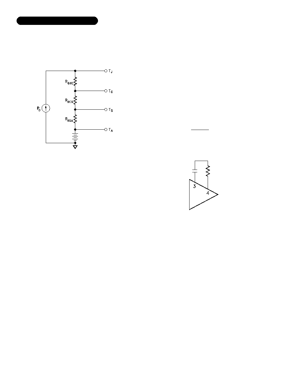
HEAT SINKING
To determine if a heat sink is necessary for your application
and if so, what type, refer to the thermal model and governing
equation below.
COMPENSATION
The MSK 032, can be frequency compensated by connecting
an R-C snubber circuit from pin 3 to pin 4 as shown below.
POWER SUPPLY BYPASSING
The recommended capacitor value is 0.01µF and the resis-
tor value can range from 2
to 500
.
The effects of this R-C
snubber can be seen on the typical performance curve labeled
Slew Rate
VS.
Compensation Resistance. The graph clearly illus-
trates the decrease in transition time as snubber resistance in-
creases. This occurs because the high frequency components
of the input square wave are above the corner frequency of the
R-C snubber and are applied common mode to the bases of the
second differential pair, (pins 3 and 4). There is no differential
gain for these higher frequencies since the input signal is ap-
plied common mode. Without the high frequency components
appearing at the output, the slew rate and bandwidth of the op-
amp are limited. However, at the cost of speed and bandwidth
the user gains circuit stability. A good design rule to follow is: as
closed loop gain decreases, circuit stability decreases, therefore
snubber resistance should decrease to maintain stability and avoid
oscillation. The MSK 032 can also be compensated using the
standard LH0032 techniques.
T
J
=P
D
X
(R
JC +
R
CS +
R
SA
)+T
A
Where
T
J=
Junction Temperature
P
D=
Total Power Dissipation
R
JC=
Junction to Case Thermal Resistance
R
CS=
Case to Heat Sink Thermal Resistance
R
SA=
Heat Sink to Ambient Thermal Resistance
T
C
= Case Temperature
T
A
= Ambient Temperature
T
S
= Sink Temperature
Governing Equation:
Conditions:
Vcc=±16VDC
Vo=±8Vp Sine Wave, Freq.= 1KHz
R
L
=510
For a worst case analysis we treat the +8Vp sine wave as an 8
VDC output voltage.
1.) Find driver power dissipation
P
D
= (Vcc-Vo) (Vo/R
L
)
Rev. B 5/02
3
Example:
This example demonstrates a worst case analysis for the op-
amp output stage. This occurs when the output voltage is 1/2
the power supply voltage. Under this condition, maximum power
transfer occurs and the output is under maximum stress.
= (
16V - 8V) (8V/510
)
=
=
=
=
=
125.5mW
2.) For conservative design, set T
J
=+125∞C
3.) For this example, worst caseT
A
=+100∞C
4.) R
JC=
187∞C/W from MSK 032B Data Sheet
5.) R
CS=
0.15∞C/W for most thermal greases
6.) Rearrange governing equation to solve for R
SA
R
SA
=
((T
J
- T
A
)/P
D
) - (R
JC
) - (R
CS
).
= ((125∞C-100∞C) /0.13W) - 187∞ C/W - 0.15∞C/W
= 192.3 - 187.15
= 5.2∞C/W
The heat sink in this example must have a thermal resistance
of no more than 5.2∞C/W to maintain a junction temperature
of no more than+125∞C.
SLEW RATE
VS
. SLEW RATE LIMIT
SLEW RATE
SR = 2
Vp
F: Slew rate is based upon the sinusoidal linear
response of the amplifier and is calculated from the full power
bandwidth frequency.
SLEW RATE LIMIT
dv/dt: The slew rate limit is based upon the amplifier's res-
ponse to a step input and is measured between 10% and 90%.
MSK measures T
R
orT
F
, whichever is greater at±10Vou
T
,
RL=510
SRL= V
O
-20%
T
R
or T
F
Both the negative and positive power supplies must be
effectively decoupled with a high and low frequency bypass
circuit to avoid power supply induced oscillation. An effective
decoupling scheme consists of a 0.1 microfarad ceramic capa-
citor in parallel with a 4.7 microfarad tantalum capacitor from
each power supply pin to ground.
Thermal Model:

