
4707 Dey Road Liverpool, N.Y. 13088
(315) 701-6751
Wave Solderable Package
All Ceramic Capacitors
Surface Mount Magnetics
Withstands 5000G
MIL STD 461C CR03 (DC-DC Converters)
80 Volt Input Transient Tolerent
No Derating - -55∞C to +125∞C
Wide Supply Range - 10V to 50V
High Isolation - 500V
High Power Density - 17W/in≥
Output Voltage Adjustment - Standard
Remote Shutdown
Operates to 11V Input at 5W
Available with 3.3V or 5V Outputs
See DAC2800s Series for 12V and 15V Versions
Available to DSCC SMD 5962-94629 and 5962-93092
MIL-PRF-38534 CERTIFIED
ISO-9001 CERTIFIED BY DSCC
M.S.KENNEDY CORP.
6W
DC-DC
CONVERTERS
DHC2800S
DESCRIPTION:
The DHC2800S series of DC-DC converters provides the ruggedness, reliability and features required to
meet the advanced design challenges of today's hi-rel market. This is accomplished while retaining a
power density of 17 W/in≥ and 425 mW/gram of power/package performance. The use of advanced
substrate and reflow soldering techniques during construction results in a rugged, cost-effective and com-
pletely solderable package.
DHC2800S hybrid converter series utilizes all ceramic capacitors and surface mount magnetics to
provide reliable operation at all operating temperatures while surviving very high G forces.
DHC2800S standard features include output fault monitoring and/or turn on voltage point programming
via the shutdown pin. All three functions may be implemented simultaneously with a minimum of external
components. An output voltage adjustment/load compensation pin is also standard.
Fault tolerant design protects these converters from most external circuit faults. The output and output
adjust pins will withstand +35V while the shutdown pin will withstand +50V protecting the converters
from a variety of system or board faults i.e. solder bridges, etc. Unique load fault protection circuitry
allows this converter to pull up loads having difficult static load line characteristics and allows short term
load excursions significantly beyond ratings in most applications.
A transformer isolated forward converter topology operating at a switching frequency of 400kHz allows
operation over a wide input voltage range. Internal filtering of both input and output eliminates the need for
external capacitors in many applications.
The 8-pin DIP package is hermetically sealed and isolated from the internal circuits. Heat sinking is
recommended for full power operation at elevated ambient temperatures.
Rev. B 6/03
1
SERIES
FEATURES:

EQUIVALENT SCHEMATIC
Isolated Step Down Power Supply
Microprocessor Power Source
Low Voltage Subsystem Power Source
TYPICAL APPLICATIONS
1
2
3
4
5
+Output
-Output
Adjust/Comp
NC
Shutdown Plus
PIN-OUT INFORMATION
Case
-Input
+Input
8
7
6
-65∞C to +150∞C
300∞C
See Efficiency Curve
150∞C
6.5∞C/W
ABSOLUTE MAXIMUM RATINGS
+50V
80V
2.0A
1.5A
-55∞C to +125∞C
-40∞C to +85∞C
Input Voltage (pin 7 to pin 6)
Input Transient (pin 7 to pin 6 @ 50mS)
Output Current
DHC2803S
DHC2805S
Case Temperature Range
DHC2800S H/E
DHC2800S
V
IN
V
INT
I
OUT
T
C
Storage Temperature Range
Lead Temperature Range
(10 Seconds)
Power Dissipation
Junction Temperature
Thermal Resistance
(Switches)
T
ST
T
LD
P
D
T
J
JC
Rev. B 6/03
2

V
IN
=16V, 28V and 40V
I
OUT
=0A, 0.8A and 1.6A
I
OUT
=0.9A to/from 1.8A
Transition TIme=30µS
I
OUT
=0.9A to/from 1.8A
Transition TIme=30µS
V
IN
=16V to/from 40V
Transition Time=30µS
V
IN
=16V to/from 40V
Transition Time=30µS
P
OUT
=6W MAX.
P
OUT
=5W MAX.
P
OUT
=2.5W MAX.
Enabled, I
OUT
=0mA
Disabled I
OUT
=0mA
No Effect on DC Performance
Input to output or any pin to case @ 500V
R
POT
=50K
12V
V
IN
50V
16V
V
IN
50V
BW=10KHz to 2MHz
BW=10KHz to 2MHz
V
IN
=16V to 40V
1
2
3
4
5
6
7
8
+V
IN
= 28V, I
OUT
= 1.8A for DHC2803S, I
OUT
= 1.0A for DHC2805S, T
A
=T
C
=25∞C unless otherwise specified.
Guaranteed by design but not tested. Typical parameters are representative of actual device performance but are for reference only.
Industrial grade and "E" suffix devices shall be tested to subgroups 1 and 4 unless otherwise specified.
Military grade devices ("H" suffix) shall be 100% tested to subgroups 1, 2, 3 and 4.
Subgroups 5 and 6 testing available upon request.
Subgroup 1, 4 T
A
=T
C
=+25∞C
2, 5 T
A
=T
C
=+125∞C
3, 6 T
A
=T
C
= -55∞C
Device has internal shutdown feature that pulses the output with a low duty cycle during faults.
Refer to DSCC SMD for electrical specifications for devices purchased as such.
ELECTRICAL SPECIFICATIONS
NOTES:
Rev. B 6/03
3
Capacitive Load
Isolation
Short Circuit Current Limit
Switching Frequency
VOUT Adjustment Range
VDC
VDC
mA
mA
mA
mA
mVp-p
mVp-p
mAp-p
mAp-p
mV
mV
mV
mV
%
%
mV
mV
µS
µS
mV
mV
µS
µS
mV
mV
mS
mS
µS
µS
mS
V
V
V
mA
mA
µF
M
A
KHz
%
Min.
3.20
3.15
152
152
152
152
-
-
-
-
-
-
-
-
61
58
-
-
-
-
-
-
-
-
-
-
-
-
-
-
-
12
11
10
-
-
-
100
2.4
375
±10
Output Voltage
Output Voltage Ripple
Input Current Ripple
Line Regulation
Load Regulation
Efficiency
Step Load Response
Step Load Recovery
Step Line Response
Step Line Recovery
Start Up Overshoot
Start Up Delay
Shutdown Delay
Parameter
Test Conditions
1
Max.
3.40
3.45
1520
1520
1820
1820
190
475
200
200
±15
±50
±25
±50
-
-
±500
±750
300
300
±500
±500
500
-
200
200
50
50
500
500
-
50
50
50
40
5
300
-
3.6
425
-
DHC2803S
DHC2803S H/E
Input Voltage Range
Output Current
Units
Typ.
3.30
-
-
-
-
-
85
-
165
-
±6
-
±10
-
66
-
±300
-
85
-
±190
-
120
-
0
0
30
-
220
-
60
-
-
-
35
2
-
-
3.1
400
-
Group A
Subgroup
1
2,3
1
2,3
1
2,3
1
2,3
1
2,3
1
2,3
1
2,3
1
2,3
4
5,6
4
5,6
4
5,6
4
5,6
4
5,6
4
5,6
4
5,6
-
1,2,3
1,2,3
1,2,3
1,2,3
1,2,3
1,2,3
1
1
4
1
7
2
Min.
3.18
-
152
-
152
-
-
-
-
-
-
-
-
-
61
-
-
-
-
-
-
-
-
-
-
-
-
-
-
-
-
12
11
10
-
-
-
100
2.4
350
±10
Max.
3.42
-
1520
-
1820
-
190
-
225
-
±20
-
±30
-
-
-
±500
-
300
-
±500
-
500
-
200
-
50
-
500
-
-
50
50
50
45
5
300
-
3.6
450
-
Typ.
3.30
-
-
-
-
-
85
-
165
-
±6
-
±10
-
66
-
±300
-
85
-
±190
-
120
-
0
-
30
-
220
-
60
-
-
-
35
2
-
-
3.1
400
-
Shutdown Recovery
Quiescent Current
2
2
2
2
2
8
2
DHC2803S
2

V
IN
=16V, 28V and 40V
I
OUT
=0A, 0.5A and 1A
I
OUT
=500mA to/from 1000mA
Transition TIme=30µS
I
OUT
=500mA to/from 1000mA
Transition TIme=30µS
V
IN
=16V to/from 40V
Transition Time=30µS
V
IN
=16V to/from 40V
Transition Time=30µS
P
OUT
=6W MAX.
P
OUT
=5W MAX.
P
OUT
=2.5W MAX.
Enabled, I
OUT
=0mA
Disabled I
OUT
=0mA
No Effect on DC Performance
Input to output or any pin to case @ 500V
R
POT
=50K
Capacitive Load
Isolation
Short Circuit Current Limit
Switching Frequency
VOUT Adjustment Range
ELECTRICAL SPECIFICATIONS
VDC
VDC
mA
mA
mA
mA
mVp-p
mVp-p
mAp-p
mAp-p
mV
mV
mV
mV
%
%
mV
mV
µS
µS
mV
mV
µS
µS
mV
mV
mS
mS
µS
µS
mS
V
V
V
mA
mA
µF
M
A
KHz
%
Min.
4.95
4.80
120
120
120
120
-
-
-
-
-
-
-
-
64
62
-
-
-
-
-
-
-
-
-
-
-
-
-
-
-
12
11
10
-
-
-
100
1.6
375
±10
Output Voltage
Output Voltage Ripple
Input Current Ripple
Line Regulation
Load Regulation
Efficiency
Step Load Response
Step Load Recovery
Step Line Response
Step Line Recovery
Start Up Overshoot
Start Up Delay
Shutdown Delay
Parameter
Test Conditions
1
Max.
5.05
5.20
1200
1200
1500
1500
190
475
200
200
±15
±50
±25
±50
-
-
±500
±750
300
300
±500
±500
500
-
200
200
50
50
500
500
-
50
50
50
40
5
300
-
2.2
425
-
DHC2805S
DHC2805S H/E
Input Voltage Range
Output Current
Units
Typ.
5.00
-
-
-
-
-
75
-
100
-
±6
-
±10
-
69
-
±300
-
90
-
±160
-
140
-
0
0
30
-
220
-
60
-
-
-
35
2
-
-
1.9
400
-
12V
V
IN
50V
16V
V
IN
50V
BW=10KHz to 2MHz
BW=10KHz to 2MHz
V
IN
=16V to 40V
I
OUT
=0A and 1A
I
OUT
=0A and 1A
Group A
Subgroup
1
2,3
1
2,3
1
2,3
1
2,3
1
2,3
1
2,3
1
2,3
1
2,3
4
5,6
4
5,6
4
5,6
4
5,6
4
5,6
4
5,6
4
5,6
-
1,2,3
1,2,3
1,2,3
1,2,3
1,2,3
1,2,3
1
1
4
1
7
2
Min.
4.90
-
120
-
120
-
-
-
-
-
-
-
-
-
64
-
-
-
-
-
-
-
-
-
-
-
-
-
-
-
-
12
11
10
-
-
-
100
1.5
350
±10
Max.
5.10
-
1200
-
1500
-
190
-
225
-
±20
-
±30
-
-
-
±500
-
300
-
±500
-
500
-
200
-
50
-
500
-
-
50
50
50
45
5
300
-
2.3
450
-
Typ.
5.00
-
-
-
-
-
75
-
100
-
±6
-
±10
-
69
-
±300
-
90
-
±160
-
140
-
0
-
30
-
220
-
60
-
-
-
35
2
-
-
1.9
400
-
Rev. B 6/03
4
Shutdown Recovery
Quiescent Current
2
2
2
2
2
8
2
DHC2805S
1
2
3
4
5
6
7
8
+V
IN
= 28V, I
OUT
= 1.8A for DHC2803S, I
OUT
= 1.0A for DHC2805S, T
A
=T
C
=25∞C unless otherwise specified.
Guaranteed by design but not tested. Typical parameters are representative of actual device performance but are for reference only.
Industrial grade and "E" suffix devices shall be tested to subgroups 1 and 4 unless otherwise specified.
Military grade devices ("H" suffix) shall be 100% tested to subgroups 1, 2, 3 and 4.
Subgroups 5 and 6 testing available upon request.
Subgroup 1, 4 T
A
=T
C
=+25∞C
2, 5 T
A
=T
C
=+125∞C
3, 6 T
A
=T
C
= -55∞C
Device has internal shutdown feature that pulses the output with a low duty cycle during faults.
Refer to DSCC SMD for electrical specifications for devices purchased as such.
NOTES:
2
APPLICATION NOTES
POWER SUPPLIES
The output voltage of the DHC2800S may be adjusted from
90% to 110% of nominal value by the use of a 50K
potenti-
ometer as shown. Adjustment beyond this range is possible
however certain characteristics of the converter such as but
not limited to input voltage range, efficiency, ripple and tem-
perature performance will change. Characterization by the user
is recommended in such applications.
Adjust/comp (pin 3) may be driven by external circuitry refer-
enced to pin 2 (-output) if desired. Grounding pin 3 causes
voltage to increase (25% typically) while driving pin 3 above
1.3V causes output voltage to decrease. Pin 3 may be driven
through 10K
or more if connection of the comp function is
also required.
The comp function of pin 3 allows capacitive loads as large
as 1000µF to be accommodated on the DHC2805S without
loss of stability. This feature may be utilized by connecting a
10nF capacitor between pins 3 and 1. This is generally recom-
mended when low ESR load capacitances of 100µF or greater
are used.
Rev. B 6/03
5
SHUTDOWN PLUS
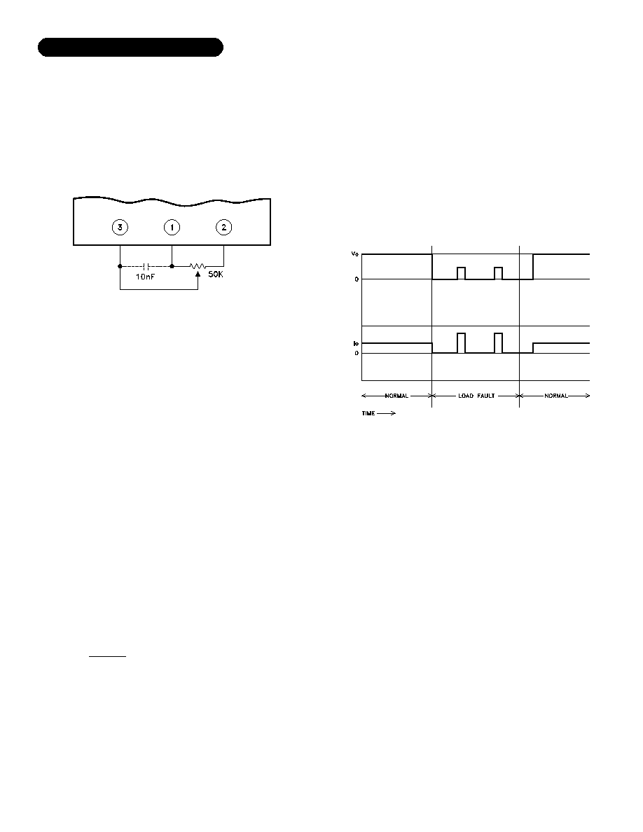
Pin 5 is used for remote shutdown, output fault detection,
and/or setting the input voltage point at which the converter
will turn on as shown in the typical application diagram. No
connection to pin 5 is necessary for normal operation of the
converter. Pin 5 is referenced to the -input (pin 7).
Shutdown may be implemented by simply connecting pin 5
to an open collector logic output or switch rated at 2.5mA,
25Vdc or higher.
Input voltage turn on point is programmed with a single resis-
tor from pin 5 to 7. An input turn on/off hysteresis (typically
3.5% of Vin) will be observed. This should be considered when
making or verifying set point adjustment. The value of the
setpoint resistor may be determined by the following:
R= (±10% accuracy at 25∞C)
Set point temperature coefficient is typically +400ppm/∞C.
Output fault monitoring is accomplished by observing pin 5
with a high impedance monitoring circuit. Pin 5 voltage drops
from over 10V to below 1V when a load fault causes the con-
verters fault protection circuitry to activate. It will remain low
for at least 100mS and return high. If the load fault is still
present pin 5 will return low and the cycle will repeat. A resis-
tor >400K
from pin 5 to 7 provides pull down for pin 5 if
there is no input setpoint programming resistor already in place.
210∑10≥
E
TO
-9.5
LOAD FAULT RESPONSE
The DHC2800S series of dc-dc converters share load fault
philosophies. Load fault conditions include short-circuit and
severe overload conditions. The DHC2800S converter series
responds to load faults by turning off all power conversion cir-
cuits for 250mS and then attempting to restart for 10mS (typi-
cal). The net "on" duty factor during a fault is very low result-
ing in low converter dissipation and immunity from overheating
at 125∞C. Current beyond rated can flow into the load at
startup time. This allows the converter to bring up capacitive
and other difficult load types more reliably than competing con-
verters.

Rev. B 6/03
6
TYPICAL APPLICATION CIRCUIT

TYPICAL PERFORMANCE CURVES
Rev. B 6/03
7
LINE TRANSIENT RESPONSE
0.0
2.0
OUTPUT CURRENT, I
OUT
(A)
10
12
14
16
LOW LINE DROP OUT
INPUT VOLTAGE, V
IN
(V)
0.5
1.0
1.5
10K
90K
60K
20K
30K 40K
INPUT VOLTAGE, V
IN
(V)
TIME, t (500
µ
sec/DIV)
LOAD TRANSIENT RESPONSE 1000
µ
F
LINE TRANSIENT RESPONSE
EFFICIENCY CONTOURS
11
30
50
40
20
OUTPUT RESPONSE, X (UNITS/DIV)
OUTPUT CURRENT, I
OUT
(A)
1.44
.18 .36
.72
1.08
1.8
1.44
.18 .36
.72
1.08
1.8
1.44
.18 .36
.72
1.08
1.8
SET POINT RESISTOR, R
SP
(
)
TIME, t (5msec/DIV)
12
16
20
24
28
TURN ON THRESHOLD
TURN ON VOLTAGE, E
TO
(V)
TURN ON RESPONSE
100 200 400
FREQUENCY, f (Hz)
≠100
AUDIO REJECTION
AUDIO REJECTION, A
V
(dB)
0
≠20
≠40
1K 2K 4K 10K 20K 40K 100K
≠60
≠80
RESPONSE, X (UNITS/DIV)
3.3V
0V
0V
28V
V
OUT
V
IN
TEMP = 25
∞
C
30%
40%
50%
55%
60%
63%
65%
67%
68%
69%
70%
INPUT VOLTAGE, V
IN
(V)
EFFICIENCY CONTOURS
OUTPUT CURRENT, I
OUT
(A)
TEMP =
125
∞
C
30%
40%
50%
55%
60%
62%
64%
65%
66%
67%
INPUT VOLTAGE, V
IN
(V)
EFFICIENCY CONTOURS
11
50
40
20
30
11
50
40
20
30
OUTPUT CURRENT, I
OUT
(A)
TEMP = ≠55
∞
C
30%
40%
50%
55%
67%
68%
68%
60%
65%
66%
63%
INCLUDES 1000
µ
F ON OUTPUT BUS
TIME, t (200
µ
sec/DIV)
TIME, t (200
µ
sec/DIV)
TIME, t (200
µ
sec/DIV)
LOAD TRANSIENT RESPONSE 100
µ
F
OUTPUT RESPONSE, X (UNITS/DIV)
OUTPUT RESPONSE, X (UNITS/DIV)
OUTPUT RESPONSE, X (UNITS/DIV)
INCLUDES 100
µ
F ON OUTPUT BUS
TIME, t (100
µ
sec/DIV)
LOAD TRANSIENT RESPONSE
OUTPUT RESPONSE, X (UNITS/DIV)
1.8A
1.8A
.9A
.9A
V
OUT
V
OUT
V
OUT
V
OUT
V
IN
V
IN
11V
16V
.9A
80V
40V
1.8A
LOAD 1.8A
V
OUT
I
OUT
I
OUT
I
OUT
1 V
500mA
1 V
500mA
100mV
20V
50mV
10V
1 V
10 V
1
V
500mA
NO OUTPUT BUS CAPCITANCE
V
IN
= 28V
I
OUT
= 2.0A
OUTPUT DC
CURRENT RATING
INCLUDES 100
µ
F ON
OUTPUT BUS
DHC2803S
V
OUT
(50mV/DIV)
V
OUT
(1V/DIV)
V
OUT
(1V/DIV)
V
OUT
(100mV/DIV)
V
OUT
(1V/DIV)
V
OUT
(1V/DIV)

TYPICAL PERFORMANCE CURVES
Rev. B 6/03
8
LINE TRANSIENT RESPONSE
0.0
1.6
OUTPUT CURRENT, I
OUT
(A)
10
12
14
16
LOW LINE DROP OUT
INPUT VOLTAGE, V
IN
(V)
0.4
0.8
1.2
10K
90K
60K
20K
30K 40K
INPUT VOLTAGE, V
IN
(V)
TIME, t (500
µ
sec/DIV)
LOAD TRANSIENT RESPONSE 1000
µ
F
LINE TRANSIENT RESPONSE
EFFICIENCY CONTOURS
11
30
50
40
20
OUTPUT RESPONSE, X (UNITS/DIV)
OUTPUT CURRENT, I
OUT
(A)
.96
.12 .24
.48
.78
1.2
SET POINT RESISTOR, R
SP
(
)
TIME, t (5msec/DIV)
12
16
20
24
28
TURN ON THRESHOLD
TURN ON VOLTAGE, E
TO
(V)
TURN ON RESPONSE
100 200 400
FREQUENCY, f (Hz)
≠100
AUDIO REJECTION
AUDIO REJECTION, A
V
(dB)
0
≠20
≠40
1K 2K
10K 20K
100K
≠60
≠80
RESPONSE, X (UNITS/DIV)
5.0V
0V
0V
28V
V
OUT
V
IN
TEMP = 25
∞
C
TEMP = 25
∞
C
30%
40%
50%
55%
60%
65%
68%
70%
71%
72%
INPUT VOLTAGE, V
IN
(V)
EFFICIENCY CONTOURS
OUTPUT CURRENT, I
OUT
(A)
TEMP =
125
∞
C
30%
40%
50%
55%
60%
63%
66%
68%
69%
70%
INPUT VOLTAGE, V
IN
(V)
EFFICIENCY CONTOURS
11
50
40
20
30
11
50
40
20
30
OUTPUT CURRENT, I
OUT
(A)
.96
.24
.12
.48
.78
1.2
.96
.24
.12
.48
.78
1.2
TEMP = ≠55
∞
C
30%
40%
50%
55%
68%
69%
70%
60%
66%
63%
INCLUDES 1000
µ
F ON OUTPUT BUS
TIME, t (200
µ
sec/DIV)
TIME, t (200
µ
sec/DIV)
TIME, t (200
µ
sec/DIV)
LOAD TRANSIENT RESPONSE 100
µ
F
OUTPUT RESPONSE, X (UNITS/DIV)
OUTPUT RESPONSE, X (UNITS/DIV)
OUTPUT RESPONSE, X (UNITS/DIV)
INCLUDES 100
µ
F ON OUTPUT BUS
INCLUDES 100
µ
F ON OUTPUT BUS
INCLUDES 100
µ
F ON OUTPUT BUS
INCLUDES 100
µ
F ON OUTPUT BUS
TIME, t (100
µ
sec/DIV)
LOAD TRANSIENT RESPONSE
OUTPUT RESPONSE, X (UNITS/DIV)
1.2A
LOAD = 1.2A
LOAD = 1.2A
LOAD = 1.2A
1.2A
600mA
600mA
V
OUT
V
OUT
V
OUT
V
OUT
V
IN
V
IN
11V
16V
600mA
80V
40V
1.2A
V
OUT
I
OUT
I
OUT
I
OUT
1 V
500mA
1 V
500mA
100mV
20V
50mV
10V
1 V
10 V
2
V
500mA
NO OUTPUT BUS CAPCITANCE
V
IN
= 28V
I
OUT
= 1.2A
OUTPUT DC
CURRENT RATING
DHC2805S
V
OUT
(50mV/DIV)
V
OUT
(1V/DIV)
V
OUT
(2V/DIV)
V
OUT
(100mV/DIV)
V
OUT
(1V/DIV)
V
OUT
(1V/DIV)

MECHANICAL SPECIFICATIONS
The information contained herein is believed to be accurate at the time of printing. MSK reserves the right to make
changes to its products or specifications without notice, however, and assumes no liability for the use of its products.
Please visit our website for the most recent revision of this datasheet.
M.S. Kennedy Corp.
4707 Dey Road, Liverpool, New York 13088
Phone (315) 701-6751
FAX (315) 701-6572
www.mskennedy.com
Rev. B 6/03
ORDERING INFORMATION
ALL DIMENSIONS ARE ±0.010 INCHES UNLESS OTHERWISE LABELED
ESD TRIANGLE INDICATES PIN 1
9
Screening Level
DHC2803S
DHC2803SE
DHC2803SH
DHC2805S
DHC2805SE
DHC2805SH
5962-93092
5962-94629
Part
Number
Industrial
Extended Reliability
Mil-PRF-38534 Class H
Industrial
Extended Reliability
Mil-PRF-38534 Class H
DSCC-SMD for DHC2805S
DSCC-SMD for DHC2805S
Output
Voltage
3.3V
5.0V