4707 Dey Road Liverpool, N.Y. 13088
M.S.KENNEDY CORP.
(315) 701-6751
FEATURES:
161
ISO-9001 CERTIFIED BY DSCC
HIGH POWER
High Output Current
Wide Supply Range
Low Cost Class "C" Output Stage
Wide Common Mode Range
Low Quiescent Current
Electrically Isolated Case
Replaces PA61
MIL-PRF-38534 QUALIFIED
DESCRIPTION:
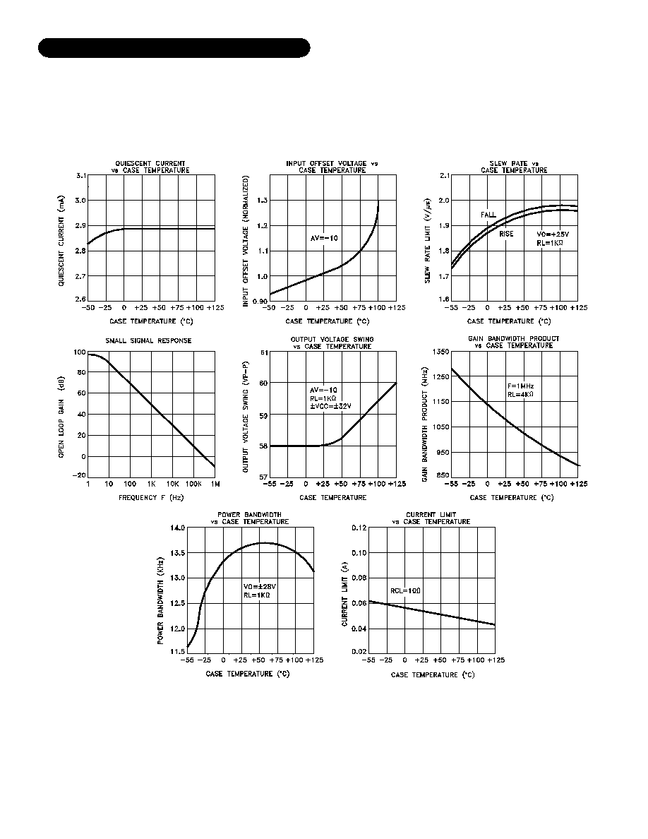
The MSK 161 is a high output current operational amplifier designed to drive resistive or reactive loads. The Class "C"
output stage is protected by a user programmable current limit scheme. The MSK 161 is designed to be a low cost solution
for low frequency applications where crossover distortion is not critical. The MSK 161 can supply ±10 amps of output
current within its safe operating range and boasts a 16 KHz power bandwidth. A low junction to case thermal resistance of
only 1.2∞C/W for the output devices keeps junction temperatures low when driving large load currents.
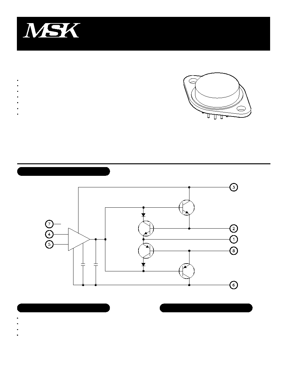
EQUIVALENT SCHEMATIC
TYPICAL APPLICATIONS
TYPICAL APPLICATIONS
PIN-OUT INFORMATION
Programmable Power Supply
Valve and Actuator Control
Motor/Syncro Driver
AC or DC Power Regulator
Output
Positive Current Limit
Positive Power Supply
Non-Inverting Input
1
2
3
4
Negative Current Limit
NC
Negative Power Supply
Inverting Input
8
7
6
5
Rev. A 6/02
1
EQUIVALENT SCHEMATIC
CLASS C AMPLIFIER
MSK 161
STATIC
Supply Voltage Range
Quiescent Current
Thermal Resistance
INPUT
Input Offset Voltage
Input Bias Current
Input Offset Current
Input Impedance
Common Mode Range
Common Mode Rejection Ratio
OUTPUT
Output Voltage Swing
Output Current, Peak
Settling Time
TRANSFER CHARACTERISTICS
Slew Rate
Open Loop Voltage Gain
Gain Bandwidth Product
Supply Voltage
Output Current
Differential Input Voltage
Case Operating Temperature Range
(MSK 161B/E) -55∞C to+125∞C
(MSK 161) -40∞C to +85∞C
Storage Temperature Range -65∞C to +150∞C
Lead Temperature Range
300∞C
(10 Seconds)
Junction Temperature 175∞C
Group A
Subgroup
-
1
2,3
-
1
2,3
1
2,3
1
2,3
-
-
-
4
4
-
4
4
-
V
mA
mA
∞C/W
mV
mV
nA
nA
nA
nA
M
V
dB
V
A
µS
V/µS
dB
MHz
V
IN
=0V
A
V
=-10V/V
F<60Hz Junction to Case
V
IN
=0V A
V
=10V/V
Bal.Pins=NC
V
CM
=0V
Either Input
V
CM
=0V
F=DC
F=1KHz V
CM
=±10V
V
CC
=±45V R
L
=1K
A
V
=-10V/V
R
CL
=0
A
V
=-10V/V T
J
<175∞C
0.1% 2V step
V
OUT
=±25V R
L
=1K
A
V
=-10V/V
V
O
=±25V R
L
=1K
F=10Hz
R
L
=1K
F=1MHz
±45V
±10A
±V
CC
-3V
±V
CC
I
OUT
V
IN
T
C
Parameter
T
ST
T
LD
T
J
ELECTRICAL SPECIFICATIONS
ABSOLUTE MAXIMUM RATINGS
Test Conditions
NOTES:
AV= -1, measured in false summing junction circuit.
Guaranteed by design but not tested. Typical parameters are representative of actual device performance but are for reference only.
Industrial grade and "E" suffix devices shall be tested to subgroups 1 and 4 unless otherwise specified.
Military grade devices ("B" suffix) shall be 100% tested to subgroups 1,2,3 and 4.
Subgroups 5 and 6 testing available upon request.
Subgroup 1,4
Subgroup 2,5
Subgroup 3,6
T
A
=T
C
=+25∞C
T
A
=T
C
=+125∞C
T
A
=T
C
=-55∞C
MSK 161B/E
Min.
±10.0
-
-
-
-
-
-
-
-
-
-
-
74
±40
±9.0
-
1.0
96
-
Typ.
-
±3.0
-
1.2
±2.0
±10.0
±12.0
-
±12.0
-
200
100
-
±10.0
2.0
2.5
100
1
Max.
±45.0
±10.0
±15.0
1.8
±6.0
±15.0
±30.0
±115.0
±30.0
±115.0
-
-
-
-
-
-
-
-
-
Typ.
-
±3.0
-
1.2
±2.0
-
±12.0
-
±12.0
-
200
100
-
10.0
2.0
2.5
100
1
MSK 161
Min.
±10.0
-
-
-
-
-
-
-
-
-
-
-
74
±40
±9.0
-
1.0
96
-
Max.
±45.0
±10.0
-
1.8
±10
-
±50
-
±50
-
-
-
-
-
-
-
-
-
-
Units
Rev. A 6/02
2
±Vcc=36VDC Unless Otherwise Specified
1
5
3
4
2
6
2
2
±V
S
-3
±V
S
-3
2
2
1
2
2
2
2
APPLICATION NOTES
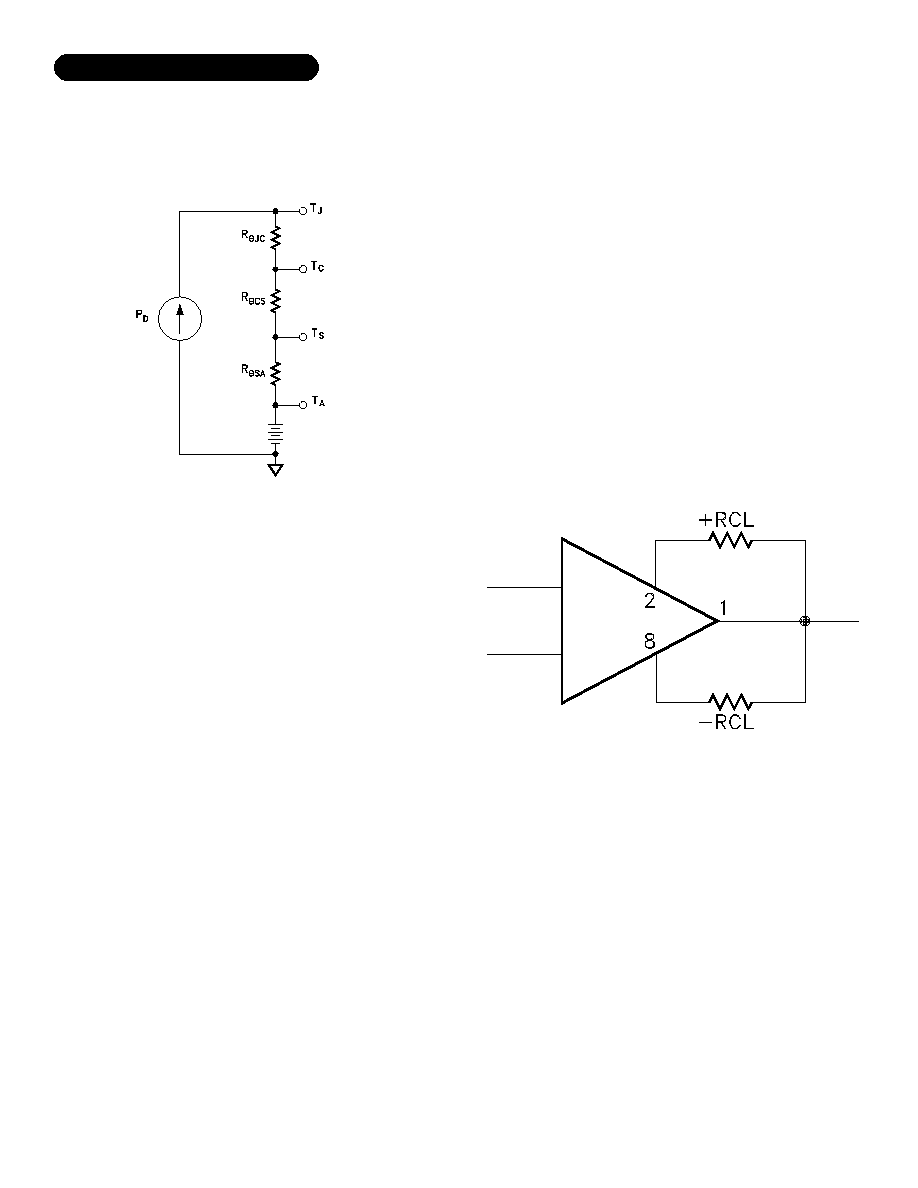
HEAT SINKING
To determine if a heat sink is necessary for your application and
if so, what type, refer to the thermal model and governing equation
below.
Governing Equation:
Example
:
In our example the amplifier application requires the output to
drive a 20 volt peak sine wave across a 400
load for 50mA of
peak output current. For a worst case analysis we will treat the
50mA peak output current as a D.C. output current. The power
supplies are ±40 VDC.
1.) Find Power Dissipation
P
D
=[(quiescent current) x (V
S
-(V
S
))]+[(+V
S
-V
O
) x I
OUT
]
=(3.0mA) x (80V)+(20V) x (1A)
=0.24W+20W
=20.24W
2.) For conservative design, set T
J
=+125∞C
3.) For this example, worst case T
A
=+50∞C
4.) R
JC
=1.8∞C/W from MSK 161 Data Sheet
5.) R
CS
=0.15∞C/W for most thermal greases
6.) Rearrange governing equation to solve for R
SA
R
SA
=((
T
J
-
T
A
)/
P
D
) - (
R
JC
) - (
R
CS
)
=((125∞C -50∞C)/20.24W) - (1.8∞C/W) - (0.15∞C/W)
=1.76∞C/W
The heat sink in this example must have a thermal resistance of
no more than 1.76∞C/W to maintain a junction temperature of no
more than +125∞C.
Rev. A 6/02
3
T
J=
P
D x
(R
JC +
R
CS +
R
SA
)
+
T
A
Where
T
J=
Junction Temperature
P
D=
Total Power Dissipation
R
JC=
Junction to Case Thermal Resistance
R
CS=
Case to Heat Sink Thermal Resistance
R
SA=
Heat Sink to Ambient Thermal Resistance
T
C=
Case Temperature
T
A=
Ambient Temperature
T
S=
Sink Temperature
Thermal Model:
CURRENT LIMIT
The MSK 161 has an on-board current limit scheme designed to
shut off the output drivers anytime output current exceeds a prede-
termined limit. The following formula may be used to determine the
value of current limit resistance necessary to establish the desired
current limit.
R
CL
=(OHMs)=(0.65 volts/current limit in amps) - 0.01OHM
The 0.01 ohm term takes into account any wire bond and lead
resistance. Since the 0.65 volt term is obtained from the base
emitter voltage drop of a bipolar transistor: the equation only holds
true for operation at +25∞C case temperature. The effect that tem-
perature has on current limit may be seen on the Current Limit vs.
Case Temperature Curve in the Typical Performance Curves.
CURRENT LIMIT CONNECTION
POWER SUPPLY BYPASSING
Both the negative and the positive power supplies must be
effectively decoupled with a high and low frequency bypass circuit
to avoid power supply induced oscillation. An effective decoupling
scheme consists of a 0.1 microfarad ceramic capacitor in parallel
with a 4.7 microfarad tantalum capacitor from each power supply
pin to ground. It is also a good practice with very high power
op-amps, such as the MSK 161, to place a 30-50 microfarad
non-electrolytic capacitor with a low effective series resistance in
parallel with the other two power supply decoupling capacitors.
This capacitor will eliminate any peak output voltage clipping which
may occur due to poor power supply load regulation. All power
supply decoupling capacitors should be placed as close to the
package power supply pins as possible (pins 7 and 12).
The information contained herein is believed to be accurate at the time of printing. MSK reserves the right to make
changes to its products or specifications without notice, however, and assumes no liability for the use of its products.
Please visit our website for the most recent revision of this datasheet.
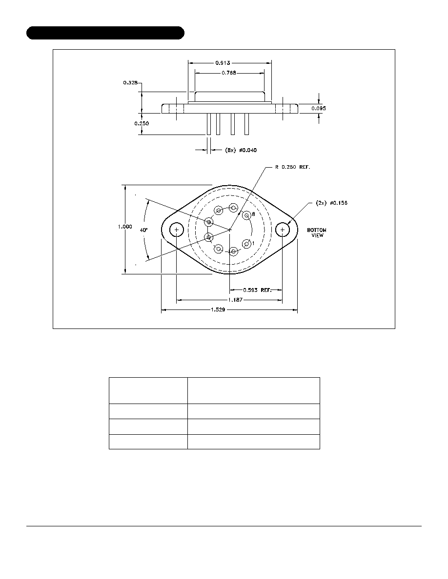
MECHANICAL SPECIFICATIONS
M.S. Kennedy Corp.
4707 Dey Road, Liverpool, New York 13088
Phone (315) 701-6751
FAX (315) 701-6752
www.mskennedy.com
NOTE: ALL DIMENSIONS ARE ±0.010 INCHES UNLESS OTHERWISE LABELED.
Rev. A 6/02
5
Screening Level
Part
Number
MSK161
MSK 161E
MSK161B
Industrial
Extended Reliability
Mil-PRF-38534 Class H
ORDERING INFORMATION
MSK 161