Half and Full Bridge Motor Drives
Audio Power Amplifiers
Headphones
Cellular Phones, PCMCIA, PDA
Ideal for Single Supply Systems
5V
- Peripheral
12V - Automotive
28V - Avionic
4707 Dey Road Liverpool, N.Y. 13088
(315) 701-6751
FEATURES:
ISO-9001 CERTIFIED BY DSCC
M.S.KENNEDY CORP.
Extremely Compact Surface Mount Package
Low Cost Dual High Power Amplifier
Wide Supply Voltage Range: 5V to 40V
High Output Current: 2A
High Efficiency: |Vs-2.2V| at 2A
Internal Current Limit
Wide Common Mode Range
(Includes Negative Supply Voltage)
Low Distortion
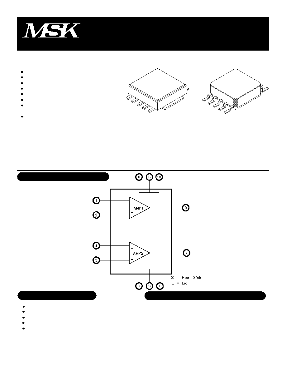
EQUIVALENT SCHEMATIC
The MSK 173 is a high power dual operational amplifier. Each amplifier is capable of delivering two amps of
current to the load. The MSK 173 is an excellent low cost alternative for bridge mode configurations since both
amplifiers are packaged together and will track thermally. The wide common mode range includes the negative rail,
facilitating single supply applications. It is possible to have a "ground based" input driving a single supply amplifier
with ground acting as the second or "bottom" supply of the amplifier. The output stage is current limit protected to
approximately 4.0 amps. The MSK 173 is packaged in an extremely space efficient 10 pin power SOIC package. The
MSK 173-1 is packaged in a 10 pin flatpack. Consult the factory for other packaging options if desired.
DESCRIPTION:
1
All power pins must be
electrically connected
for proper operation.
PIN-OUT INFORMATION
1
2
3
4
5
-Input 1
+Input 1
-Vcc
+Input 2
-Input 2
+Vcc
Output 1
+Vcc
Output 2
+Vcc
Rev. H 8/00
The heat sink of the package and the lid are electrically
connected to -Vcc. The heat sink tab must be connected
to the system -Vcc.
HEAT SINK
10
9
8
7
6
TYPICAL APPLICATIONS
173/173-1
HIGH POWER DUAL
OPERATIONAL AMPLIFIER
MSK173
MSK173-1
MIL-PRF-38534
1
2
3
4
5
6
STATIC
Supply Voltage Range
INPUT
Offset Voltage Drift
Power Supply Rejection
Common Mode Rejection
Total Noise
OUTPUT
Output Voltage Swing
Output Current Peak
Current Limit
Power Bandwidth
Crosstalk
Capacitive Load
TRANSFER CHARACTERISTICS
Slew Rate
Open Loop Voltage Gain
(Split Supply)
Total; V
IN
=0V
V
IN
=0V
V
CM
=0V
Full Temp.
V
CC
=�15V
V
CM
=�10VDC
R
L
=500
A
V
=1 C
L
=1500pF
V
OUT
=MAX
V
OUT
=28V
PP
I
OUT
=1A f=1KHz
A
V
=+1V/V
F=10Hz R
L
=500
-65�C to +150�C
300�C
-55�C to+125�C
-40�C to +85�C
3.0�C/W
12.0�C/W
Storage Temperature
Lead Temperature
Case Operating Temperature
(MSK173B,173B-1 )
(MSK173,173-1)
Thermal Resistance (DC)
Junction to Case
MSK 173
MSK 173-1
Total Supply Voltage
Output Current (within S.O.A.)
Input Voltage (Differential)
Input Voltage
(Common Mode)
Junction Temperature
40V
3A PK
�V
CC
+V
CC
, -V
CC
-0.5V
150�C
ABSOLUTE MAXIMUM RATINGS
T
ST
T
LD
T
C
R
TH
V
CC
�I
OUT
V
IND
V
IN
T
J
Unless otherwise noted �V
CC
=�15VDC.
Devices shall be capable of meeting the parameter, but need not be tested. Typical parameters are for reference only.
Industrial grade devices shall be tested to subgroups 1 and 4 unless otherwise requested.
Military grade devices ('B' suffix) shall be 100% tested to subgroups 1,2,3 and 4. Consult factory for availability of military grade devices.
Subgroup 5 and 6 testing available upon request.
Subgroup 1,4 T
C
=+25�C
Subgroup 2,5 T
C
=+125�C
Subgroup 3,6 T
A
=-55�C
Group A
Subgroup
-
1
2
3
1
2, 3
-
-
-
-
-
-
4
-
-
-
-
-
4
-
Typ.
�15
�35
�50
�30
�0.5
�2.0
�20
�35
�75
80
85
0.1
�14.2
�3.0
�4.0
13.6
68
0.22
1.2
100
Min.
�2.5
-
-
-
-
-
-
-
-
60
60
-
�14
�2.0
-
-
60
-
0.5
80
Min.
�2.5
-
-
-
-
-
-
-
-
60
60
-
�14
�2.0
-
-
-
-
0.5
80
Max.
�20
�60
-
-
�15
-
-
�1000
-
-
-
1.0
-
-
-
-
-
-
-
-
Typ.
�15
�35
-
-
�2
-
�20
�35
�75
80
85
0.1
�14.2
�3.0
�4.0
13.6
68
0.22
1.2
100
Units
V
mA
mA
mA
mV
mV
�V/�C
nA
nA
dB
dB
mV
V
A
A
KHz
dB
�F
V/�S
dB
Parameter
Max.
�20
�50
�75
�50
�10
�15
�50
�500
�1000
-
-
1.0
-
-
-
-
-
-
-
-
Test Conditions
ELECTRICAL SPECIFICATIONS
NOTES:
Quiescent Current
V
IN
=0V
Offset Voltage
Input Bias Current
2
4
4
MSK173
MSK173-1
2
2
2
2
2
2
2
2
2
1
2
MSK173B
MSK173B-1
Rev. H 8/00
APPLICATION NOTES
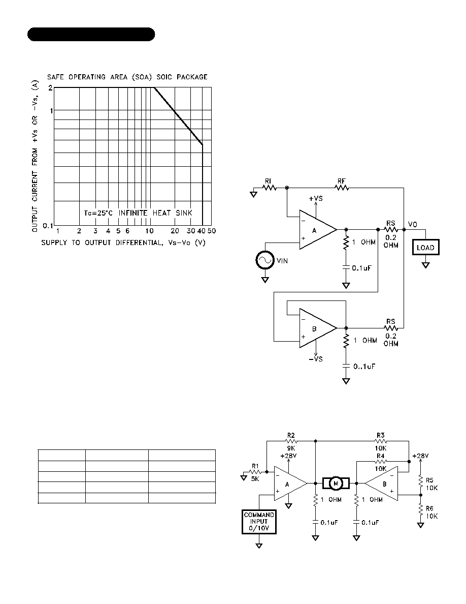
SAFE OPERATING AREA (SOA)
AMPLIFIER STABILITY
Since both output transistors in this amplifier are NPN, consid-
eration must be taken when stabilizing the output. A one ohm
resistor, 0.1uF capacitor snubber network should be added ex-
ternally from the output to -Vcc on each amplifier. This con-
figuration minimizes local output stage oscillations. As always,
adequate power supply bypassing is a necessity for ampli-
fier stability. A parallel combination of a 4.7uF electrolytic (for
every amp of output current) and a 0.01uF ceramic disc capaci-
tor should be connected as close as possible to the package
power supply pins to ground.
If the inductive load is driven near steady state conditions al-
lowing the output to drop more than 6V below the supply rail
while the amplifier is current limiting, the inductor should be
capacitively coupled or the supply voltage must be lowered to
meet the SOA criteria. It is a good practice to also connect
reverse biased fast recovery diodes to the output for protection
against sustained high energy flyback.
�Vcc
20V
15V
10V
5V
Capacitive Load
200uF
500uF
5mF
50mF
Inductive Load
7.5mH
25mH
35mH
150mH
Safe operating area curves are a graphical representation of all
of the power limiting factors involved in the output stage of an
operational amplifier. Three major power limiting factors are;
output transistor wire bond carrying capability, output transis-
tor junction temperature and secondary breakdown effects. To
see if your application is meeting or exceeding the limitations
of the safe operating area curves, perform the following steps:
1. Find the worst case output power dissipation. For a split
supply, purely resistive load application, this occurs when
V
OUT
=1/2 V
CC
.
2. Take the values of (V
CC
-V
OUT
) and the corresponding out-
put current and find their intersection on the safe operating
area curves.
3. Verify this point is below the safe operating area curves.
This is a simple task for purely resistive loads, for reactive loads
the following table will save extensive analysis. Under tran-
sient conditions, capacitive and inductive loads up to the fol-
lowing maximum are usually safe.
PARALLEL CONNECTION
yields single 4A amplifier
BIDIRECTIONAL MOTOR DRIVE
3
Rev. H 8/00
APPLICATION NOTES CONTINUED
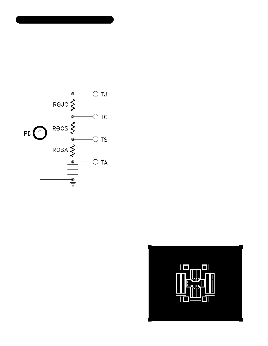
HEAT SINKING
To determine if a heat sink is necessary for your applica-
tion and if so, what type, refer to the thermal model and
governing equation below.
Thermal Model:
1.) Find Driver Power Dissipation
P
D
= [(quiescent current) x (+V
CC
- (-V
CC
))] +
[(V
CC
-V
O
) x I
OUT
]
= (75mA) x (24V) + (2V) x (0.5A) + (2V) x (0.5A)
= 1.8W + 2W
= 3.8W
2.) For conservative design, set T
J
=+150�C.
3.) For this example, worst case T
A
=+25�C
4.) R
JC
= 3.0�C/W
5.) Rearrange governing equation to solve for R
SA
R
SA
= ((T
J
- T
A
)/P
D
) - (R
JC
) - (R
CS
)
= ((150�C - 25�C) / 3.8W) - (3�C/W)
29.9�C/W
The heat sink in this example must have a thermal resis-
tance of no more than 30�C/W to maintain a junction
temperature of no more than +150�C
.
Example:
In our example the amplifier application requires each out-
put to drive a 10 volt peak sine wave across a 20 ohm
load for 0.5 amp of output current. For a worst case
analysis we will treat the 0.5 amp peak output current as
a D.C. output current. The power supplies are �12VDC.
The device is the SOIC version.
UNIVERSAL EVALUATION PC BOARD LAYOUT
The MSK 173 is a highly thermally conductive device and
the thermal path from the package to the internal junc-
tions is very short. Standard surface mount techniques
should be used when soldering the device into a circuit
board. A hole can be cut in the printed circuit board to
allow the heat sink of the package to be thermally bonded
to an external heat sink for high power applications.
Governing Equation:
T
J
= P
D
x (R
JC
+ R
CS
+ R
SA
) + T
A
Where
T
J
= Junction Temperature
P
D
= Total Power Dissipation
R
JC
= Junction to Case Thermal Resistance
R
CS
= Case to Heat Sink Thermal Resistance
R
SA
= Heat Sink to Ambient Thermal Resistance
T
C
= Case Temperature
T
A
= Ambient Temperature
T
S
= Sink Temperature
The heat sink and lid of the MSK 173 are electrically con-
nected to the negative power supply rail. The user is
urged to keep this in mind when designing the printed
circuit card the MSK 173 will be placed in. There should
be no printed circuit traces making contact with the case
of the device except for -Vcc. The -Vcc plane or ground
for single supply systems, can be used to pull heat away
from the device and must be connected electrically to the
heat sink.
DEVICE SOLDERING
CASE CONNECTION
4
Rev. H 8/00
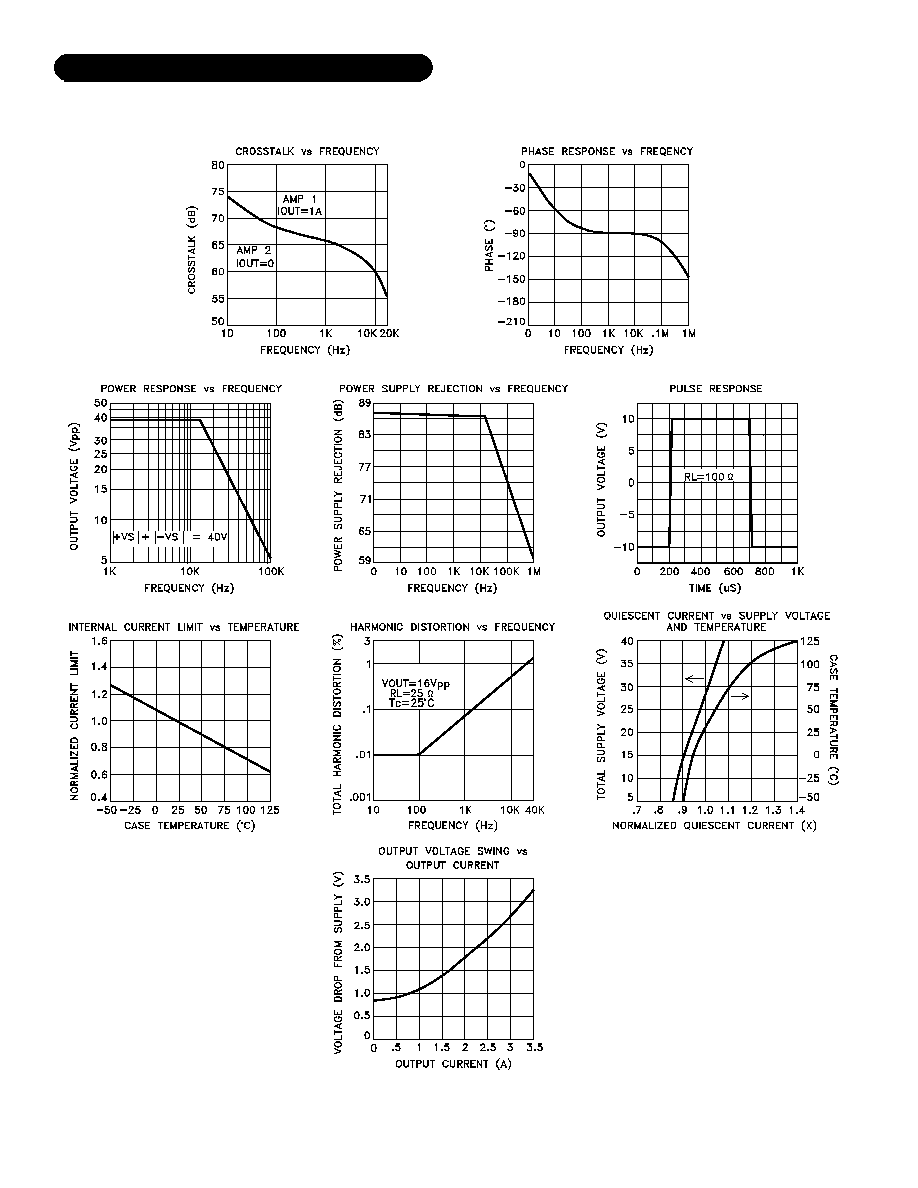
TYPICAL PERFORMANCE CURVES
5
Rev. H 8/00