 | –≠–ª–µ–∫—Ç—Ä–æ–Ω–Ω—ã–π –∫–æ–º–ø–æ–Ω–µ–Ω—Ç: MSK1901E | –°–∫–∞—á–∞—Ç—å:  PDF PDF  ZIP ZIP |

V
OFF
V
REF
Ground
Ground
Ground
Ground
NC
NC
Output
NC
V
CB
V
CB
PIN-OUT INFORMATION
TYPICAL APPLICATIONS
4707 Dey Road Liverpool, N.Y. 13088
(315) 701-6751
FEATURES:
MIL-PRF-38534 QUALIFIED
ISO-9001 CERTIFIED BY DSCC
DESCRIPTION:
1
2
3
4
5
6
7
8
9
10
11
12
Ground
Ground
Ground
Ground
Blank
V
CC
V
EE
V
EE
-Input
+Input
Ground
V
GAIN
13
14
15
16
17
18
19
20
21
22
23
24
User Adjustable Brightness and Contrast
25,000 V/µSec Slew Rate
Available to DSCC SMD 5962-9324601HX
The MSK 1901 is a high performance, high voltage, variable gain video amplifier. The hybrid's open collector output
is capable of directly driving a high resolution video display.
The MSK 1901 features differential inputs and a linearly adjustable gain stage with an output offset adjustment which
allows it to be a versatile performer well suited for many applications. A TTL level blanking input is available to set the
output to a predetermined black level independent of signal output.
The MSK 1901 is packaged in a hermetically sealed 24 pin quad flat pack with mounting flanges that can be
conveniently connected to a heat sink.
EQUIVALENT SCHEMATIC
High Resolution Mono-Chrome Displays
High Resolution RGB Displays
High Speed, High Voltage Amplification for ATE
Ultra Fast Rise Time - 2.8nS Typical
Wide Bandwidth - 225 MHz Typical
Variable Gain - 0 to 80 V/V
On Board Reference Output
50 V
PP
Output Voltage Swing
Blanking Capability
Rev. A 5/02
1
M.S.KENNEDY CORP.
1901
HIGH SPEED/HIGH VOLTAGE
VIDEO DISPLAY DRIVER

STATIC
High Voltage Supply (WRT
V
CB
)
Thermal Resistance
INPUT
V
CM
=0V@+10V
V
CM
=0V@-10.5V
T
C
125∞C
Junction To Case
V
BLANK
=0.4V
V
BLANK
=2.4V
V
OFF
=1V
V
GAIN
=5V
Normal Operation
V
CM
=±0.5V F=10Hz
Either Input F=DC
Either Input
V
BLANK
=2.4V V
IN
=0.3V
V
GAIN
=5V
+V
CC
and -V
CC
=Nom ±5%
I
OUT
<2mA
V
BLANK
=2.4V V
OFF
=1V V
GAIN
=0V
V
OFF
=0V V
GAIN
=4V
V
OFF
=5V V
GAIN
=0V
Test Conditions
Storage Temperature Range
Lead Temperature Range
(Solder 10 Seconds)
Junction Temperature
Total Power Dissapation
+65V
+12V
-12V
+20V
2V
-0.6V to +6V
-0.6V to +6V
-0.6V to +6V
5mA
High Voltage Supply (WRT V
CB
)
P
ositive Supply Voltage
Negative Supply Voltage
Common Base Supply Voltage
Differential Input Voltage
Gain Adjust Input Voltage
Offset Adjust Input Voltage
Blank Input Voltage
Reference Output Current
-65∞C to +150∞C
+300∞C
+175∞C
13W
ABSOLUTE MAXIMUM RATINGS
T
ST
T
LD
+V
HV
Group A
Subgroup
1,2,3
1,2,3
-
-
1
2,3
1
1
1
1
-
-
-
-
-
-
-
1,2,3
1,2,3
1,2,3
1,2,3
4
1,2,3
-
4
-
-
-
Typ.
55
75
60
5
±1
±5
500
300
2
2
-
40
20
2
-
-
30
5.5
0
10
100
500
30
225
2.8
-
-
-
Min.
-
-
20
-
-
-
-
-
-
-
30
-
10
-
-
-
25
5.2
-2
0.5
80
395
-
200
-
-
-
-
Units
mA
mA
V
∞C/W
µA
µA
µA
µA
µA
µA
nS
dB
K
pF
mA
mA
dB
V
mA
mA
mA
mS
mA
MHz
nS
%GS
%
%GS
MSK1901B
Max.
70
100
65
7
±50
±250
600
400
10
10
-
-
-
-
±2
±10
-
5.8
2
25
120
605
40
-
4.5
±2
±2
±2
ELECTRICAL SPECIFICATIONS
1
2
3
4
5
6
7
+V
CC
=+10V, -V
EE
=-10.5V, +V
HV
=+70V, V
CB
=+10V, V
BLANK
=0.4V, C
L
=6pF, R
L
=200
, V
GAIN
=V
OFF
=±V
IN
=0V unless otherwise specified.
Guaranteed by design but not tested. Typical parameters are representative of actual device performance but are for reference only.
Much faster rise times are obtainable without using test sockets. In addition, a peaking network may be used to improve overall bandwidth.
Industrial grade and "E" suffix devices shall be tested to subgroups 1 and 4 unless otherwise specified.
Military grade devices ("B" suffix) shall be 100% tested to subgroups 1,2,3 and 4.
Subgroups 5 and 6 testing available upon request.
Subgroup 1,4 T
C
=+25∞C
Subgroup 2,5 T
C
=+125∞C
Subgroup 3,6 T
A
=-55∞C
NOTES:
Quiescent Current
Parameter
1
Rev. A 5/02
2
Input Bias Current
Offset Adjust Input Current
Gain Adjust Input Current
Blank Input Pulse Width
Common Mode Rejection Ratio
Input Impedence
Input Capacitance
Blank Mode Input Rejection
mA
Gain Adjust Rejection
mA
Power Supply Rejection Ratio
OUTPUT
Reference Output Voltage
Output Current Blank Mode
Output Current Min Offset
Output Current Max Offset
Transconductance
Common Base Current
Bandwidth
Transition Times
Linearity Error
Gain Linearity
Thermal Distortion
V
IN
=0.6V F=10KHz V
GAIN
=5V Both Inputs
V
CM
=0V
V
OFF
=0V R
L
=50
V
IN
=0.6V V
GAIN
=4V T
R
=T
F
<1nS V
OFF
=1V
V
GAIN
=1V V
OFF
=1V V
CM
=0.5V
V
OFF
=1V V
IN
=0.2V V
CM
=0.5V
-
V
GAIN
V
OFF
V
BLANK
I
REF
T
J
V
CM
=0V
+V
CC
-V
EE
V
CB
V
ID
(T
C
=25∞C)
-55∞C to +125∞C
-40∞C to +85∞C
Case Operating Temperature Range
(MSK 1901B/E)
(MSK1901)
T
C
P
D
Blank Input Current
2
2
2
2
2
2
2
2
3
2
2
2

APPLICATION NOTES
INITIAL SETUP
It is important to set the V
OFF
and V
GAIN
inputs to ob-
tain balanced rise/fall times during initial setup of the
MSK 1901. If the
quiescent current level of V
OFF
is set
too low, it will slow the
rise time and limit the bandwidth
of the MSK 1901.
VIDEO INPUTS
The analog inputs (±
V
IN
) are designed to accept RS343
signals, ±0.714V
PP
, and will operate properly with a com
-
mon mode range of ±0.5V with respect to ground. There-
fore, it is recommended that the input signal be limited
to ±1.3V with respect to ground, (signal+common
mode). Although large offsets of ±2V (with respect to
ground, signal included) can be tolerated without dam-
age to the hybrid, output linearity suffers and therefore it
is not recommended.
V
GAIN
V
GAIN
is the DC gain (contrast) control which varies the
gain from 0 to 80V/V. The internal reference (V
REF
) is
available to drive this input. Normally a 5K potentiometer
is connected between V
REF
and GND is used to vary the
gain, but any 0-5V external DC source may be used with
some additional degredation of gain stability over tem-
perature. A 0.1µF capacitor should be connected from
the V
GAIN
pin to ground to improve stability.
The gain equation for the MSK 1901 is:
V
LRS
-
V
O
=V
IN
x
G
M
x
R
L
=V
IN
(V
GAIN
x
0.08) R
L
The overall gain of the MSK 1901 may vary by ±20%
due to process variations of the internal components.
Temperature variations also effect gain, <150ppm/∞C.
If more than one MSK 1901 is used in a system, steps
should be taken to make them track thermally (i.e. a
common heat sink). This will reduce any mismatches due
to varying temperatures.
V
OFF
V
OFF
is the output offset (brightness) control used to
set the output quiescent current and consequently the
DC output voltage (black level). Output quiescent cur-
rent adjustment range is from several µA to 100mA nomi-
nal (80 to 130mA actual). Normally a 5K potentiometer
is
connected between V
REF
and GND to this input, but
any 0-5V external DC source may be used. A 0.1µF ca-
pacitor should be connected from this pin to signal ground
to improve the amplifier's stability.
BLACK LEVEL
The voltage developed across the external load resis-
tor with a 0V video input to the MSK 1901 is the black
level. This voltage may be changed by adjusting the load
resistor or by varying the output quiescent current of the
MSK 1901as described
in V
OFF
above. The black level
could also be affected by the V
GAIN
control voltage if the
video input has a DC component. AC coupling of the
video input will prevent this phenomenon from occuring.
BLANKING
The blank input is a TTL active high input. When active
it will disable the video input of the MSK 1901 and allow
the output to rise to approximately V
LRS
.
If the blank in-
put rises above 3V some interaction between V
OFF
and
BLANK level may occur. The BLANK input is indepen-
dent of the input signal and must be tied "low" to acti-
vate the amplifier if the blanking function is not used.
V
REF
OUTPUT
V
REF
is a buffered zener reference with a nominal out-
put voltage of 5.5V ±5% which can source up to 4mA.
It is available for use in adjusting the offset and gain. If
multiple amplifiers are used for RGB amplification, they
should all
share the same V
REF
pin from one of the hy-
brids. The V
REF
pin should be buffered with a unity gain
precise amplifier when driving three amplifiers for RGB
applications.
V
CB
The V
CB
input is the base connection to the output
stage consisting of a common base, high voltage stage
and a high speed, low voltage current amplifier in a
cascode arrangement. This input requires a very stable
10V DC nominal voltage. Any AC signals at this point
will be amplified and reflected in the output. The PSRR
of the output stage is directly related to the stability of
this VCB voltage.
VIDEO OUTPUT
The video output voltage is obtained from the open
collector of a cascode circuit designed to operate with a
nominal output
supply (V
LRS
) of +70V. V
LRS
must be
greater
than the applied V
CB
voltage, but less than V
CB
+65V. The output of MSK 1901 will drive loads up to
250mA when proper heat sinking is used.
Rev. A 5/02
3
APPLICATION NOTES CON'T
Rev. A 5/02
4
OUTPUT CONNECTIONS
In applying the MSK 1901 in a system, two challenges
present themselves. The first challenge is to minimize
any stray capacitance from the output pin to ground.
Since the output connection is extremely susceptible to
capacitance loading, the elimination of ground planes
adjacent to the output and resistive load are important or
the rise and fall times will be limited. Keep output con-
nections as short as possible and insure that any ground
plane is at least one inch from the output signal.
The second challenge is to provide a very low
impedence connection between two sets of ground pins
(1, 2, 3, 4 and 15, 16, 17, 18). If mounting permits, the
best solution is to run a board ground track under the
MSK 1901 connecting the adjacent ground pins. How-
ever, the standard practice of heat sinking the MSK 1901
directly to the CRT chassis usually precludes this. A cut-
out is usually provided in the PC board where the MSK
1901 is surface mounted on the opposite side from the
other components. Two suggestions for this surface
mounting technique to improve performance are directed
at functionality or speed.
A functional solution is to run a ground trace on the
output pin side of the hybrid on the back side of the PC
board. The trace should be 0.1 to 0.2 inch necking down
to 0.1 inch as it perpendicularly crosses the output trace
on the other side of the board. This results in added
capacitance of only 0.1 to 0.4 pF.
A high speed solution is to have the ground cross the
input pin side of the hybrid. To counter the signal ground
disruption, the signal ground (pin 11) is internally con-
nected to the (15, 16, 17, 18) grounds. Use as broad a
ground trace as possible to improve stability.
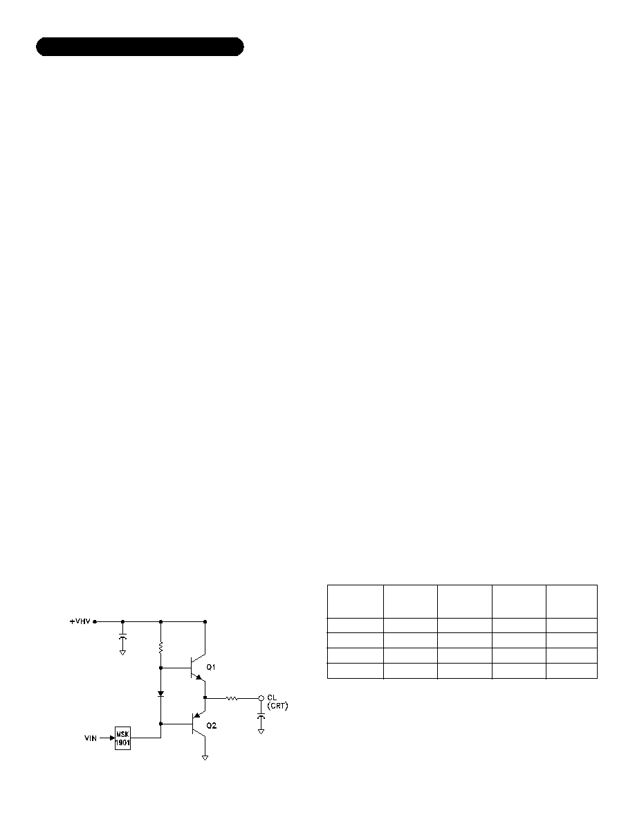
A third suggestion is to buffer the MSK 1901 using a
differential follower stage. This configuration as shown
in Figure 1 below allows an easier layout which mini-
mizes stray capacitance. The rise time is essentially lim-
ited by the capacitance of the output transistor and that
of Q1 and Q2.
Figure 1
POWER SUPPLIES
A +10V and a -10.5V power supply are required for
proper operation. These supplies can be set at ±12V for
convenience but this will increase the internal power dis-
sipation and package case temperature. V
LRS
can be any
voltage above V
CB
but not greater than V
CB
+65V. To
achieve maximum performance good high frequency
grounding practices and PC board layout are essential.
Proper power supply decoupling is also essential for
stability and good video performance. Place bypass ca-
pacitors as close to power supply pins as possible. Refer
to the typical connection circuit for recommended con-
nections.
POWER SUPPLY SEQUENCING
Power supply sequencing is necessary to avoid inter-
nal latch-up of the hybrid. External diodes should be placed
(anode to cathode) from V
EE
to GND, from GND to V
CC
and from V
CC
to V
LRS
. If power supply sequencing is not
possible, all supplies should be applied to the hybrid within
5 mS of each other.
POWER DISSIPATION
The MSK 1901 power dissipation will vary depending
on load requirements and speed. The quad flat pack of
the hybrid is designed to provide a low thermal resis-
tance path from the hybrid circuit to an external heat
sink. Mounting flanges provide for excellent mechanical
and thermal attachment of the package to the heat sink.
In addition, the package is electrically isolated so that
mounting insulators are not needed and the heat sink
can be at any convenient potential. Refer to the follow-
ing table for typical power levels for selected video con-
ditions:
POWER DISSIPATION TABLE
(T
C
=25∞C, V
LRS
=70V, R
L
=200
)
V
O
-V
BLACK
Duty
Cycle %
IC P
D
Watts
P
LOAD
Watts
TOTAL
P
D
Watts
0
100
80
80
0
35
35
50
1.6
7.8
6.5
5.6
0
6.1
4.9
10
1.6
13.9
11.4
15.6
When using multiple MSK 1901's, attach all devices
to a common heat sink (e.g. in a RGB system). This al-
lows close thermal tracking between hybrids and improves
color balance with varying input drive and ambient tem-
perature conditions. Common thermal tracking of the
devices reduces timing and other errors found in RGB
systems.

TYPICAL CONNECTION CIRCUIT
Rev. A 5/02
5
The connection circuit shown above is for the MSK 1901. The R
L
and L
P
are external components and must
not be located near ground planes if possible. A high quality resistor such as Bradford Electronics P/N FP10-200
is reqired for optimum response times. Use an inductor with a high self-resonant frequency that can withstand
the currents required for the application. The ferrite beads should be located as close to the DUT as possible.
Fare-Rite Corporation P/N 2743001111 beads work well for most applications. For additional applications informa-
tion, please contact MSK. Evaluation amplifiers with test boards are readily available upon request.
NOTES:
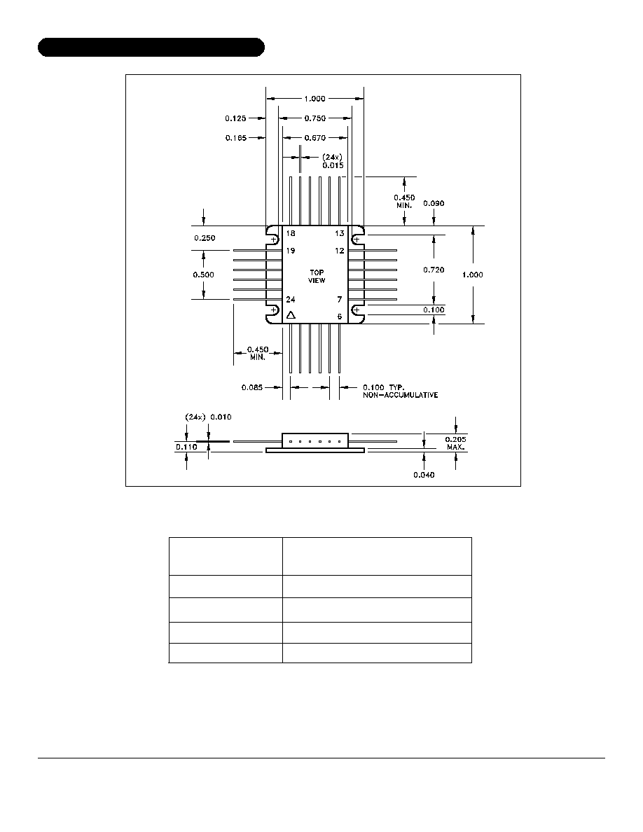
MECHANICAL SPECIFICATIONS
ESD TRIANGLE INDICATES PIN 1.
ALL DIMENSIONS ARE ±0.010 INCHES UNLESS OTHERWISE LABELED.
Rev. A 5/02
The information contained herein is believed to be accurate at the time of printing. MSK reserves the right to make
changes to its products or specifications without notice, however, and assumes no liability for the use of its products.
Please visit our website for the most recent revision of this datasheet.
M.S. Kennedy Corp.
4707 Dey Road, Liverpool, New York 13088
Phone (315) 701-6751
FAX (315) 701-6752
www.mskennedy.com
MSK1901
Screening Level
Part
Number
MSK1901
MSK1901B
MSK1901E
5962-9324601HX
Industrial
Military-Mil-PRF-38534 Class H
Extended Reliability
DSCC-SMD
ORDERING INFORMATION
5