4707 Dey Road Liverpool, N.Y. 13088
(315) 701-6751
FEATURES:
100V
PP
Output Signal Into 10
P
F
Ultra Fast Transition Times-2.9nS
User Adjustable Contrast and Brightness
TTL Compatible Blanking
On Board DC Reference Output
Customized Versions Available Upon Request
Available to DSCC SMD 5962-9324301HX
MIL-PRF-38534 CERTIFIED
ISO-9001 CERTIFIED BY DSCC
M.S.KENNEDY CORP.
1903
DESCRIPTION:
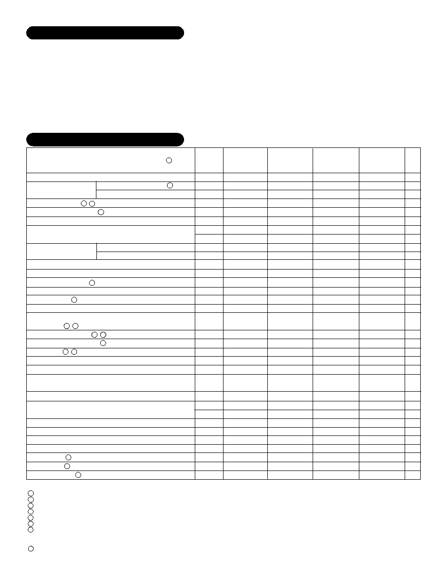
The MSK 1903 Series of high speed, high voltage video amplifiers was designed to drive the grid of today's high
performance CRT's. The MSK 1903 has user adjustable contrast and brightness levels and also comes with a blanking
function. The MSK 1903 can be directly connected to many video sources including RS170, RS343 and high speed
video D/A converters. The MSK 1903 is available in four versions for different applications. The MSK 1903-0 has no
internal high voltage resistor or inductor allowing the user to dissipate much of the power externally. The MSK 1903-
2, MSK 1903-4 and the MSK 1903-6 each have an internal resistor-inductor designed for optimum bandwidth. The
MSK 1903-6 has slightly lower bandwidth but can be operated from down to -120V. Each version of the MSK 1903
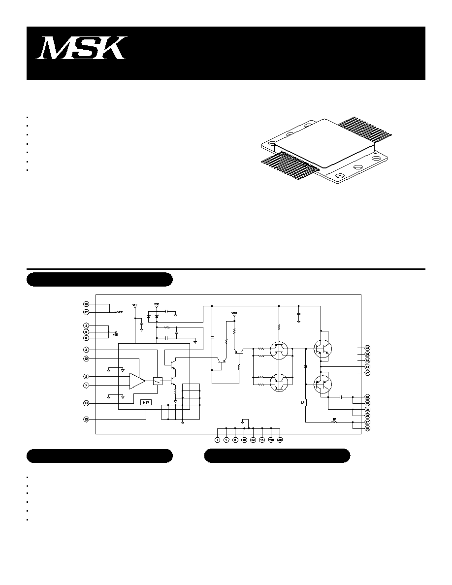
is packaged in a 30 pin power flatpack that can be directly connected to a heat sink using standard 4-40 screws.
EQUIVALENT SCHEMATIC
Helmet Mounted Displays
High Resolution RGB Displays
High Resolution Monochrome Displays
Automatic Test Equipment
Beam Index Applications
Projection Displays
TYPICAL APPLICATIONS
1
2
3
4
5
6
7
8
9
10
GND
GND
Blank
V
EE
V
EE
V
EE
-Input
+Input
GND
GND
PIN-OUT INFORMATION
-V
HV
NC
Output
NC
NC
NC
V
CC
V
CC
GND
GND
21
22
23
24
25
26
27
28
29
30
V
GAIN
V
OFF
V
REF
GND
GND
-V
HV
RES
-V
HV
RES
GND
GND
-V
HV
11
12
13
14
15
16
17
18
19
20
HIGH SPEED/HIGH VOLTAGE
NEGATIVE OUTPUT
VIDEO AMPLIFIER
Rev. B 3/03
1
SERIES
+V
CC
= +20V, -V
EE
= -10.5V, V
BLANK
=0.4V V
GAIN
= V
OFF
= �V
IN
= 0V, C
L
=10pF, V
HV
=typical value and T
C
=25�C unless otherwise specified.
Guaranteed by design but not tested. Typical parameters are representative of actual device performance but are for reference only.
R
P
=Internal R
P
except MSK 1903-0. External value = 400
unless otherwise specified for the MSK 1903-0.
Industrial grade and "E" suffix devices shall be tested to subgroups 1 and 4 unless otherwise specified.
Military grade devices ("B" suffix) shall be 100% tested to subgroups 1,2,3 and 4.
Subgroups 5 and 6 testing available upon request.
Subgroup 1,4 T
A
=T
C
=+25�C
2,5 T
A
=T
C
=+125�C
3,6 T
A
=T
C
=-55�C
Does not include output current referenced to +V
CC
.
Rev. B 3/03
2
-95V
-95V
-75V
-120V
+22V
-12V
2V
�2V
-0.6 to +6V
-0.6 to +6V
High Voltage Supply (1903-0)
(1903-2)
(1903-4)
(1903-6)
Positive Supply Voltage
Negative Supply Voltage
Differential Input Voltage
Common Mode Input Voltage
Gain Adjust Input Voltage
Offset Adjust Input Voltage
-0.6 to +6V
5mA
-65�C to +150�C
300�C
175�C
290mA
-55�C to +125�C
-40�C to +85�C
ABSOLUTE MAXIMUM RATINGS
1
2
3
4
5
6
7
8
-V
HV
+V
CC
-V
EE
V
IN
V
IC
V
GAIN
V
OFF
Blank Input Voltage
Reference Output Current
Storage Temperature Range
Lead Temperature Range
(10 Seconds)
Junction Temperature
Current Through Rp
Case Operating Temperature Range
(All Devices B/E Suffix)
(All Devices No Suffix)
V
BLANK
I
REF
T
ST
T
LD
T
J
I
RP
T
C
ELECTRICAL SPECIFICATIONS
NOTES:
mA
mA
V
�C/W
�A
�A
�A
�A
�A
�A
nS
dB
K
pF
mV
dB
V
V
V
V
V/V
V
V
nS
%GS
%
%GS
Min.
-
-
-30
-
-
-
-
-
-
-
30
-
10
-
-
25
190
5.2
0
16
16
36
-65
-
-
-
-
-
Max.
100
-100
-95
35
�50
�250
600
400
10
10
-
-
-
-
-
420
5.8
10
52
52
138
-
-5
5.5
�2
�2
�2
STATIC
High Voltage Supply
Thermal Resistance to Case
INPUT
Offset Adjust Input Current
Gain Adjust Input Current
Blank Input Pulse Width
Common Mode Rejection Ratio
Input Impedance
Input Capacitance
Blank Mode Input
Rejection
V
Gain Adjust Rejection
V
Power Supply Rejection Ratio
Internal Rp
OUTPUT
Reference Output Voltage
V Min Offset
Voltage Gain
Output Voltage High
Output Voltage Low
Transition Times
Linearity Error
Gain Linearity
Thermal Distortion
Parameter
V
CM
=0V @ +20V
V
CM
=0V @ -10.5V
T
C
125�C
Junction to Case
V
BLANK
=0.4V
V
BLANK
=2.4V
V
OFF
=1V
V
GAIN
=5V
Normal Operation
V
CM
=�0.5V F=10Hz
Either Input F=DC
Either Input
V
BLANK
=2.4V V
IN
=0.3V
V=V
HV
-V
OUT
V
GAIN
=5V
+V
CC
and -V
EE
=Nom �5%
I
OUT
<2mA
V=V
HV
-V
OUT
V
OFF
=1V
V
BLANK
=2.4V V
GAIN
=5V
V=V
HV
-V
OUT
V
OFF
=0V V
GAIN
=3V
V
IN
=0.6V F=10KHz V
GAIN
=3V Both Inputs
V
GAIN
=3V F=10KHz
V
GAIN
=3V F=10KHz
V
IN
=0.6V V
OUT
=Max TR=TF<1nS
V
GAIN
=4V V
OFF
=1V V
CM
=0.5V
V
OFF
=1V V
IN
=0.2V V
CM
=0.5V
Test Conditions
1
Max.
100
-100
-120
35
�50
�250
600
400
10
10
-
-
-
-
-
420
5.8
10
52
52
145
-
-5
10
�2
�2
�2
Typ.
75
-75
-100
32
�1
�5
500
300
2
2
-
40
20
2
-
30
400
5.5
3
42
42
120
-98
-1
6.5
-
-
-
Min.
-
-
-50
-
-
-
-
-
-
-
30
-
10
-
-
25
380
5.2
0
32
32
72
-95
-
-
-
-
MSK1903-6
Max.
100
-100
-75
35
�50
�250
600
400
10
10
-
-
-
-
-
210
5.8
6
26
26
68
-
-5
4.0
�2
�2
�2
Typ.
75
-75
-70
32
�1
�5
500
300
2
2
-
40
20
2
-
30
200
5.5
3
21
21
55
-68
-1
2.9
-
-
-
MSK1903-4
Typ.
75
-75
-90
32
�1
�5
500
300
2
2
-
40
20
2
-
30
400
5.5
3
42
42
110
-88
-1
3.8
-
-
-
Min.
-
-
-30
-
-
-
-
-
-
-
30
-
10
-
-
25
380
5.2
0
32
32
72
-85
-
-
-
-
MSK1903-2
Max.
100
-100
-95
35
�50
�250
600
400
10
10
-
-
-
-
-
-
5.8
10
52
56
138
-
-5
6.0
�2
�2
�2
Typ.
75
-75
-90
32
�1
�5
500
300
2
2
-
40
20
2
-
30
0
5.5
3
42
42
110
-88
-1
4.2
-
-
-
Min.
-
-
-30
-
-
-
-
-
-
-
30
-
10
-
-
25
-
5.2
0
32
28
72
-85
-
-
-
-
-
MSK1903-0
mV
-
-
�2xRp
-
-
�2xRp
-
-
�2xRp
-
-
�2xRp
3xRp
Rp
-3xRp
3xRp
Rp
-3xRp
3xRp
Rp
-3xRp
3xRp
Rp
-3xRp
mV
2
3
2
2
2
2
3
2
3
Quiescent Current
Input Bias Current
Blank Input Current
V Blank Mode
V Max Offset
�10xRp
�10xRp
�10xRp
�10xRp
2
3
2
2
Group A
Subgroup
1,2,3
1,2,3
-
-
1
2,3
1
1
1
1
-
-
-
-
-
-
-
1,2,3
1,2,3
1
2,3
4
4
4
4
-
-
-
1,2,3
-
Units
V
CM
=0V
V=V
HV
-V
OUT
V
OFF
=5V
2
2
8

APPLICATION NOTES
POWER SUPPLIES
The input stage of the MSK 1903 requires power supplies of
+20V and -10.5V for optimum performance. The negative
power supply can be increased to -12V if -10.5V is not avail-
able, but additional power dissipation will cause the internal
temperature to rise. Both low voltage power supplies should be
effectively decoupled with tantalum capacitors (at least 4.7�F)
connected as close to the amplifier's pins as possible. The MSK
1903 has internal 0.01�F capacitors that also improve high
frequency performance. In any case, it is also recommended to
put 0.1�F decoupling capacitors on the +20V and -10.5V sup-
plies as well.
The high voltage power supply (-V
HV
) is connected to the
amplifier's output stage and must be kept as stable as possible.
The internal or external Rp is connected to -V
HV
and as such,
the amplifier's DC output is directly related to the high voltage
value. The -V
HV
pins of the hybrid should be decoupled to ground
with as large a capacitor as possible to improve output stabil-
ity.
VIDEO OUTPUT
When power is first applied and V
IN
=V
GAIN
=V
OFF
=0V, the
output will be practically at the -V
HV
rail voltage. The output
voltage is a function of the value of Rp and also the V
GAIN
and
V
OFF
DC inputs. The maximum output voltage swing for any of
the MSK 1903 variants is determined by Vpp = (250mA) x
(Rp). The bandwidth of the amplifier largely depends on both
Rp and Lp.
Hybrid pins 16 and 17 are directly connected to Rp. Addi-
tional external resistance can be added to reduce power dissi-
pation, but slower transition times will result. If an additional
resistor is used, it must be low capacitive and the layout should
minimize capacitive coupling to ground (ie: no ground plane
under Rp).
The MSK 1903 Series is conservatively specified with low
values for Lp which yield about 5% overshoot. Additional peak-
ing can be obtained by using a high self-resonant frequency
inductor in series with the Rp pins. Since this value of induc-
tance can be very dependent on circuit layout, it is best to
determine its value by experimentation. A good starting point
is typically 0.47�H for the MSK 1903-0 and 0.0047�H for the
remaining devices.
If external resistors or inductors are not used, be sure to
connect high frequency bypass capacitors directly from pins
16 and 17 to ground.
The V
GAIN
control (contrast) input is designed to allow the
user to vary the video gain. By simply applying a DC voltage
from 0V to V
REF
, the video gain can be linearly adjusted from 0
to 80V/V. The V
GAIN
input should be connected to the V
REF
pin
through a 5K
pot to ground. For convenient stable gain adjust-
ment, a 0.1�F bypass capacitor should be connected near the
V
GAIN
input pin to prevent output instability due to noisy sources.
Digital gain control can be accomplished by connecting a D/A
converter to the V
GAIN
pin. However, some temperature track-
ing performance may be lost when using an external DC voltage
source other than V
REF
for gain adjustment.
The overall video output of the MSK 1903 can be character-
ized using the following expression:
Vpp=V
HV
-V
OUT
V
HV
-V
OUT
=(V
IN
) (V
GAIN
) (0.1) (Rp) (0.9)
Here is a sample calculation for the MSK 1903-2:
Given information:
V
IN
=0.7V
V
GAIN
=1VDC
Rp=400
(internal)
V
HV
=100VDC
V
HV
-V
OUT
=(0.7V) (1V) (0.1) (400
) (0.9)
V
HV
-V
OUT
=25.2V Nominal
The expected video output would swing from approximately
-80V to -54.8V assuming that V
OFF
=0V. This calculation should
be used as a nominal result because the overall gain may vary as
much as �20% due to internal high speed device variations.
Changing ambient conditions can also effect the video gain of
the amplifier by as much as 150 PPM/�C. It is wise to connect
all video amplifiers to a common heat sink to maximize thermal
tracking when multiple amplifiers are used in applications such
as RGB systems. Additionally, only one of the V
REF
outputs should
be shared by all three amplifiers. This voltage should be buffered
with a suitable low drift op-amp for best tracking performance.
V
GAIN
CONTROL INPUT
OUTPUT PROTECTION
The output pin of the MSK 1903 should be protected from
transients by connecting reverse biased ultra-low capacitance
diodes from the output pin to both -V
HV
and ground. The out-
put can also be protected from arc voltages by inserting a small
value (50-100
) resistor in series with the amplifier. This resis-
tor will reduce system bandwidth along with the load capaci-
tance, but a series inductor can reduce the problem substan-
tially.
VIDEO INPUTS
The video input signals should be kept below �2V
MAX
total,
including both common mode offset and signal levels. The in-
put structure of the MSK 1903 was designed for �0.714Vpp
RS343 signals. If either input is not used it should be con-
nected directly to the analog ground or through a 25
resistor
to ground if input offset currents are to be minimized.
SUPPLY SEQUENCING
The power supply sequence is -V
HV
, V
CC
, V
EE
followed by
the other DC control inputs. If power supply sequencing is not
possible, the time difference between each supply should be
less than five milliseconds. If the DC control signals are being
generated from a low impedance source other than the V
REF
output, reverse biased diodes should be connected from each
input (V
GAIN
, V
OFF
) to the +V
CC
pin. This will protect the in-
puts until +V
CC
is turned on.
Rev. B 3/03
3
Required Rise Time
at CRT
APPLICATION NOTES CON'T
V
OFF
CONTROL INPUT
The brightness (output offset) can be linearly adjusted by
applying a 0 to V
REF
DC voltage to the V
OFF
input pin. The
output quiescent voltage range is from approximately (5�A)
(Rp) to (100mA) (Rp) from -V
HV
. This control voltage is nor-
mally generated by connecting the V
OFF
control pin to a 5K
potentiometer between V
REF
and ground. The V
OFF
input pin
should be bypassed with a 0.1�F capacitor to ground placed as
close as possible to the hybrid. This DC voltage can be any
stable system source.
Keep hybrid power dissipation in mind when adjusting the
output quiescent voltage. Practically all of the voltage is seen
across Rp. This power must be taken into account when high
Rp currents are used. If the quiescent level is set too close to
-V
HV
, the power dissipation will be minimal but the rise time
will suffer slightly. If the quiescent level is set too far from
-V
HV
, the power dissipation will increase dramatically and the
output fall time will be limited. The output black level is obvi-
ously dependent on system requirements but a little experi-
mentation will strike the optimum balance between power dis-
sipation and bandwidth. Total current through Rp should be
limited to less than 290mA when operating from power sup-
plies greater than 90V. The gain adjust alone can set the AC
current to 250mA (ie: 250mApp=100Vpp/400
). This would
leave about 40mA left for black level output current.
BLANK INPUT
The video input can be electrically disconnected from the
amplifier by applying a TTL high input to the blank pin. When
this occurs, the output will be set to approximately -V
HV
. The
V
GAIN
and V
OFF
control pins have little or no effect on the out-
put when it is in blank mode.
When the TTL compatible blank input is not used, the pin
must be connected to ground to enable the amplifier. The blank
input will float high when left disconnected which will disable
the video.
V
REF
OUTPUT
The MSK 1903 has an on board buffered DC zener reference
output. The V
REF
output is nominally 5.5V DC and has full tem-
perature test limits of 5.2V to 5.8V DC. This output is provided
for gain and offset adjustment and can source up to 4mA of
current.
THERMAL MANAGEMENT
The MSK 1903 package has mounting holes that allow the
user to connect the amplifier to a heat sink or chassis. Since
the package is electrically isolated from the internal circuitry,
mounting insulators are not required or desired for best thermal
performance. Use 4 to 6 inch/pounds for mounting the device
to the heat sink.
The power dissipation of the amplifier depends mainly on the
load requirements, bandwidth, pixel size, black level and the
value of Rp. The following table illustrates a few examples:
320 x 200
640 x 350
640 x 480
800 x 560
1024 x 900
1024 x 1024
1280 x 1024
1664 x 1200
2048 x 2048
4096 x 3300
Maximun
Pixel
Time
182nS
52nS
38nS
26nS
12.6nS
11nS
8.9nS
5.8nS
2.8nS
860pS
Minimum Pixel
Clock
Frequency
5MHz
19MHz
26MHz
38MHz
80MHz
90MHz
112MHz
170MHz
360MHz
1.2GHz
60nS
17nS
12.5nS
8.6nS
4.2nS
3.7nS
2.9nS
1.9nS
1nS
280pS
Required System
Bandwidth
(F
-3dB
)
6MHz
20MHz
28MHz
41MHz
84MHz
95MHz
120MHz
180MHz
380MHz
1.23GHz
RESOLUTION TABLE FOR A TYPICAL CRT
All data assumes retrace time equal to 30% of frame time and a 60Hz refresh rate.
This table does not include power dissipation due to output switching since this is dependent on individual load requirements. The input stage power
dissipation is typically 2.5 watts and is essentially independent of output levels.
Display
Resolution
Rev. B 3/03
4
1903-6
1903-6
1903-4
1903-4
-120V
-120V
-70V
-70V
0W
13.3W
0W
8.4W
2.5W
15.7W
2.5W
10.6W
WHITE
0%
40%
0%
40%
BLANK
100%
20%
100%
20%
0V
-90V
0V
-50V
-20V
-20V
-15V
-15V
-110V
-110V
-65V
-65V
-VHV
BLACK
0%
40%
0%
40%
PERCENT OF SIGNAL
TYPE
DEVICE
LEVEL
BLACK
LEVEL
WHITE
VOLTAGE
OUTPUT
AVE. Pd
OUTPUT
AVE. Pd
TOTAL
NOTES:
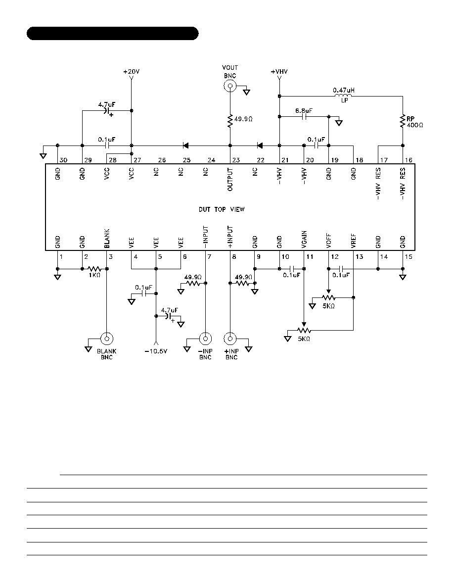
The connection circuit shown above is for the MSK 1903-0 evaluation board. The Rp and Lp are external compo-
nents and must not be located near ground planes if possible. A high quality resistor such as Bradford Electronics
P/N FP10-400 is required for optimum response times. Use an inductor with a high self-resonant frequency that can
withstand the currents required for the application.
When using the other variants of the MSK 1903, place an additional bypass capacitor on pins 16 and 17 if series
(Rp and Lp) components are not utilized. The pin should connect to -V
HV
with a short low impedance path.
For additional applications information, please contact MSK. Evaluation amplifiers with test boards are available
upon request.
TYPICAL CONNECTION CIRCUIT
Rev. B 3/03
5