Group A
Subgroup
-
1, 2, 3
1
2, 3
1
2, 3
1
2, 3
-
-
-
-
4
5, 6
4
5, 6
-
4
4
4
5, 6
-
-
-
-
-
Parameter
STATIC
Supply Voltage Range
Quiescent Current
INPUT
Input Offset Voltage
Input Offset Voltage Drift
Input Capacitance
Input Impedance
Common Mode Rejection Ratio
Power Supply Rejection Ratio
OUTPUT
Settling Time
Power Bandwidth
TRANSFER CHARACTERISTICS
Slew Rate
THERMAL RESISTANCE
JC (Junction to Case)
JC
JC
JC
JA (Junction to Ambient)
Test Conditions
Total - Both Amplifiers V
IN
= 0V
V
IN
= 0V
V
IN
= 0V
V
CM
= 0V
Either Input
F = DC
F = DC V
CM
= ±22V
V
CC
= ±10V to ±40V
R
L
= 5.6
F
10 KHz
R
L
= 10
F = 10 KHz
R
L
= 5.6
F
10 KHz
R
L
= 10
F = 10 KHz
0.1% 2V step
R
L
= 10
V
O
= 20 V
RMS
V
OUT
= ±10V R
L
= 10
One Amplifier, DC Output
One Amplifier, AC Output F > 60 Hz
Both Amplifiers, DC Output
Both Amplifiers, AC Output F
>
60 Hz
No Heat Sink
Max.
±40
±60
±10
-
±100
-
30
-
-
-
-
-
-
-
-
-
-
-
-
-
-
1.9
1.5
1.2
1.0
-
Typ.
±35
±40
±1.0
±15
±4
±10
2.0
-
5
10
12
113
90
±29
-
±8
-
2
50
10
100
-
1.4
1.25
0.9
0.8
30
Min.
±10
-
-
-
-
-
-
-
-
-
90
-
±28
-
±5
-
-
40
6
90
-
-
-
-
-
-
Typ.
±35
±40
±0.1
±15
±4
±10
2.0
-
5
10
12
113
90
±29
±31
±8
-
2
55
10
100
-
1.4
1.25
0.9
0.8
30
Min.
±10
-
-
-
-
-
-
-
-
-
95
-
±28
±30
±5
±3.0
-
45
6
95
85
-
-
-
-
-
±V
CC
Voltage Supply
±40V
I
OUT
Peak Output Current
See S.O.A.
V
IN
Differential Input Voltage
±V
CC
V
IN
Common Mode Input Voltage
±V
CC
T
C
Case Operating Temperature Range
MSK 2541B
-55∞ to +125∞C
MSK 2541
-40∞ to +85∞C
ABSOLUTE MAXIMUM RATINGS
T
ST
Storage Temperature Range
-65∞ to +150∞C
T
LD
Lead Temperature Range 300∞C
(10 Seconds)
P
D
Power Dissipation 125W
T
J
Junction Temperature 150∞C
Units
V
mA
mV
µV/∞C
pA
nA
pA
nA
pF
W
dB
dB
V
V
A
A
µS
KHz
V/µS
dB
dB
∞C/W
∞C/W
∞C/W
∞C/W
∞C/W
2
Rev. B 8/00
ELECTRICAL SPECIFICATIONS
Military
Industrial
4
3 4
Max.
±40
±60
±1.0
±30
±50
±50
30
20
-
-
-
-
-
-
-
-
-
-
-
-
-
1.9
1.5
1.2
1.0
-
NOTES:
1
Unless otherwise specified: R
CL
= 0
, ±V
CC
= ±34 V
DC
, all specs are per amplifier.
2
Electrical specifications are derated for power supply voltages other than ±34 V
DC
.
3
AV = -1, measured in false summing junction circuit.
4
Devices shall be capable of meeting the parameter, but need not be tested. Typical parameters are for reference only.
5
Industrial grade devices shall be tested to subgroups 1 and 4 unless otherwise specified.
6
Military grade devices ('B' suffix) shall be 100% tested to subgroups 1, 2, 3 and 4.
7
Subgroup 5 and 6 testing available upon request.
8
Subgroup 1, 4
T
A
=T
C
=+25∞C
Subgroup 2, 5
T
A
=T
C
=+125∞C
Subgroup 3, 6
T
A
=T
C
=-55∞C
4
2
4
4
Input Bias Current
Input Bias Current
V
CM
= 0V
Output Current
Output Voltage Swing
Open Loop Voltage Gain
F = 10 Hz R
L
= 10 K
MSK 2541B
MSK 2541
4
5
APPLICATION NOTES
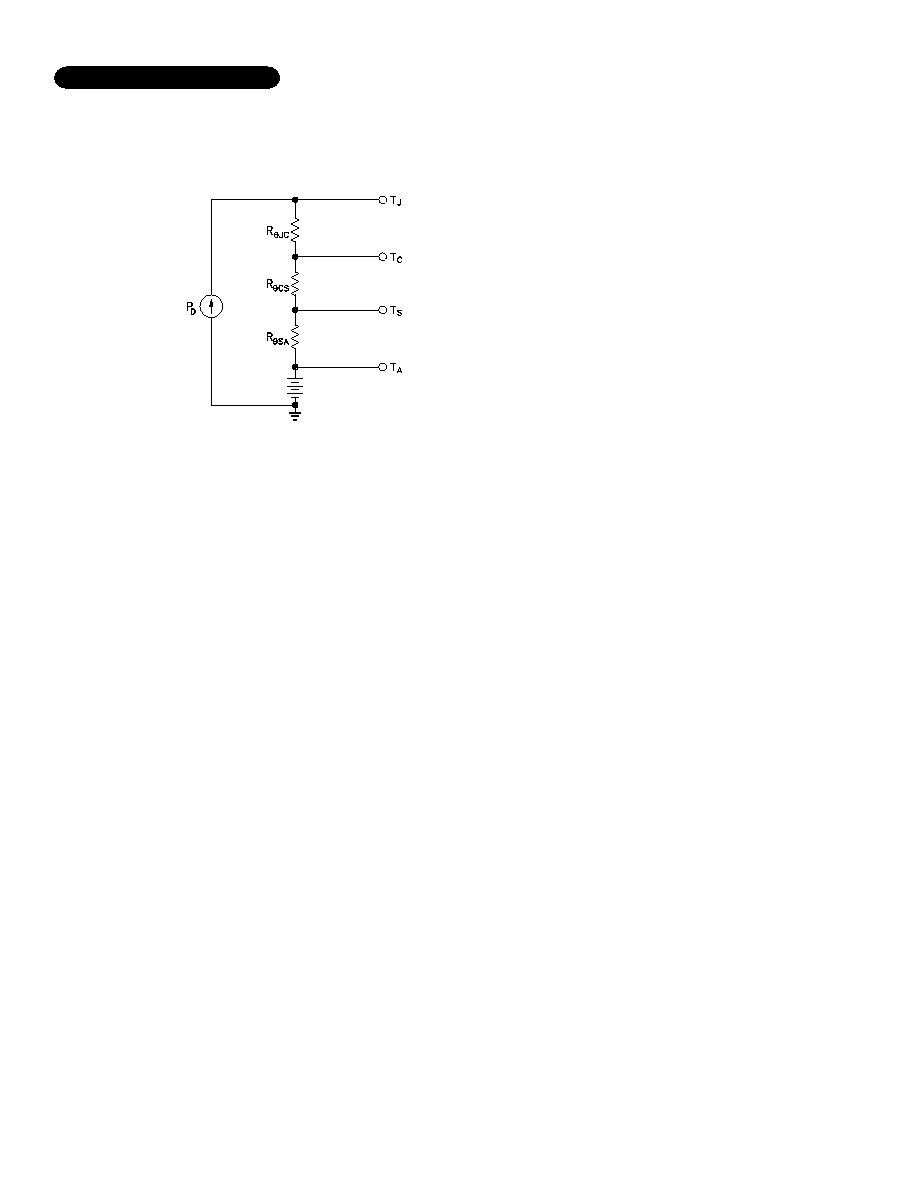
HEAT SINKING
To select the correct heat sink for your application, refer to the
thermal model and governing equation below.
Thermal Model:
Governing Equation:
T
J
= P
D
X (R
JC
+ R
CS
+ R
SA
) + T
A
Where
T
J
= Junction Temperature
P
D
= Total Power Dissipation
R
JC
= Junction to Case Thermal Resistance
R
CS
= Case to Heat Sink Thermal Resistance
R
SA
= Heat Sink to Ambient Thermal Resistance
T
C
= Case Temperature
T
A
= Ambient Temperature
T
S
= Sink Temperature
Example:
In our example the amplifier application requires each output to
drive a 20 volt peak sine wave across a 10 ohm load for 2 amps of
output current. For a worst case analysis we will treat the 2 amps
peak output current as a D.C. output current. The power supplies
are ±35 VDC.
1.) Find Power Dissipation
P
D
= [(quiescent current) X (+V
CC
- (-V
CC
))] + [(V
CC
- V
O
) X I
OUT
]
= (30 mA) X (70V) + (15V) X (2A)+(15V)x(2A)
= 2.1W + 60W
= 62.1W
2.) For conservative design, set T
J
= +150∞C
3.) For this example, worst case T
A
= +25∞C
4.) R
JC
= 1.2∞C/W typically
5.) R
CS
= 0.15∞C/W for most thermal greases
6.) Rearrange governing equation to solve for R
SA
R
SA
= (T
J
- T
A
) / P
D
- (R
JC
) - (R
CS
)
= (150∞C - 25∞C) / (62.1W) - (1.2∞C/W) - (.15∞C/W)
=
.66∞C/W
The heat sink in this example must have a thermal resistance of
no more than .66∞C/W to maintain a junction temperature of no
more than +150∞C. Since this value of thermal resistance may be
difficult to find, other measures may have to be taken to decrease
the overall power dissipation. Refer to the "Heat Sinking Options"
application note offered by MSK.
POWER SUPPLY CONNECTIONS
The MSK 2541 maximum supply voltage is specified as
±40V. However, single sided or unbalanced power supply
operation is permissible as long as the total power supply volt-
age does not exceed 80V. Caution should be exercised when
routing high current printed circuit paths. Generally, these
paths should not be placed near low level, high impedance
input circuitry to avoid oscillations.
During prototype evaluation, power supply current limiting
is strongly advised to avoid damaging the device. See the
application note entitled "Current Limit" for an explanation of
the limitations of the MSK 2541 on board current limit.
POWER SUPPLY BYPASSING
Both the negative and the positive power supplies must be
effectively decoupled with a high and low frequency bypass
circuit to avoid power supply induced oscillation. An effective
decoupling scheme consists of a 0.1 microfarad ceramic ca-
pacitor in parallel with a 4.7 microfarad tantalum capacitor
from each power supply pin to ground. It is also a good prac-
tice with very high power op-amps, such as the MSK 2541, to
place a 30-50 microfarad non-electrolytic capacitor with a low
effective series resistance in parallel with the other two power
supply decoupling capacitors. This capacitor will eliminate
any peak output voltage clipping which may occur due to poor
power supply load regulation. All power supply decoupling
capacitors should be placed as close to the package power
supply pins as possible (pins 3 and 6).
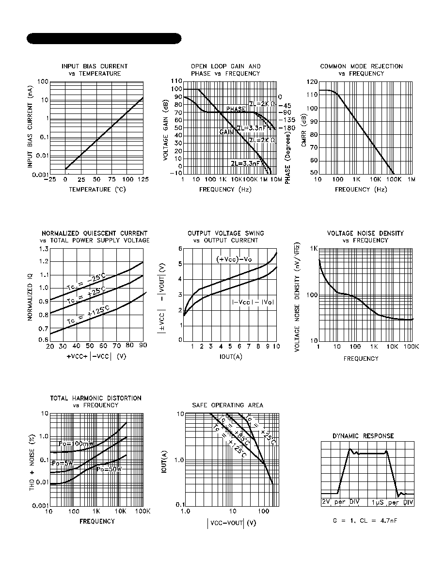
CURRENT LIMIT
The internal current limit should not be used as a short cir-
cuit protection scheme. When the output is directly shorted
to ground, the power supply voltage is applied across the out-
put transistor that is conducting. If the power supplies were
set to ±40V and the output was shorted to ground, the tran-
sistor that is conducting current would see 40V from its emit-
ter to its collector. Referring to the safe operating area curve
shows when [V
CC
-V
OUT
]=40V, the maximum safe output
current (I
O
) at T
C
=25∞C is 1.5A. In this case the amplifier
would not be protected by the internal current limit and would
probably be damaged. The internal current limit is provided as
a protection against unintentional load conditions which may
require larger amounts of load current than the amplifier is
rated for.
SAFE OPERATING AREA
The safe operating area curve is a graphical representation
of the power handling capability of the amplifier under various
conditions. The wire bond current carrying capability, transis-
tor junction temperature and secondary breakdown limitations
are all incorporated into the safe operating area curves. All
applications should be checked against the S.O.A. curves to
ensure high M.T.T.F.
3
Rev. B 8/00