 | –≠–ª–µ–∫—Ç—Ä–æ–Ω–Ω—ã–π –∫–æ–º–ø–æ–Ω–µ–Ω—Ç: MSK4304ES | –°–∫–∞—á–∞—Ç—å:  PDF PDF  ZIP ZIP |
FEATURES:
75V, 10 Amp Capability
Ultra Low Thermal Resistance - Junction to Case - 1.5∞C/W (Each MOSFET)
Self-Contained, Smart Lowside/Highside Drive Circuitry
Bootstrap High-Side Supplies
Under-Voltage Lockout
Capable of Switching Frequencies to 25KHz
Isolated Case Allows Direct Heat Sinking
Bolt-down Design Allows Superior Heat Dissipation
DESCRIPTION:
The MSK 4303 is a 10 Amp, 3 Phase Bridge Smart Power Motor Drive Hybrid with a 75 volt rating on the output
switches. The output switches are MOSFETs. This new smart power motor drive hybrid is 5.0 volt input logic
compatible. Under-voltage lockout shuts down the bridge when the supply voltage gets to a point of incomplete
turn-on of the output switches. The internal high-side bootstrap power supply derived from the +VB supply
completely eliminates the need for 3 floating independent power supplies.
4707 Dey Road Liverpool, N.Y. 13088
(315) 701-6751
MIL-PRF-38534 CERTIFIED
ISO-9001 CERTIFIED BY DSCC
Rev. B 11/05
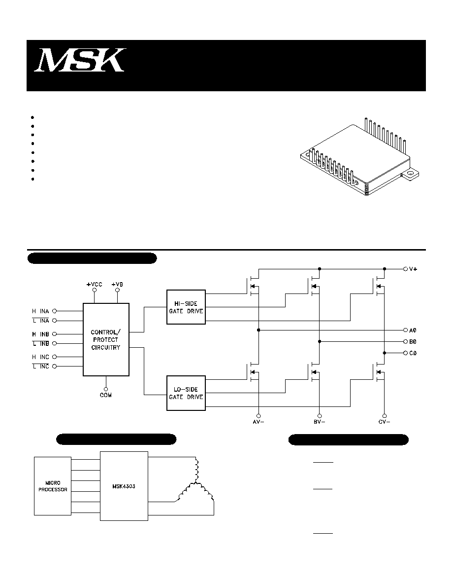
TYPICAL APPLICATIONSPIN-OUT INFORMATION
TYPICAL APPLICATIONS
PIN-OUT INFORMATION
3 PHASE SIX STEP DC BRUSHLESS MOTOR DRIVE
OR 3 PHASE SINUSOIDAL INDUCTION MOTOR DRIVE
EQUIVALENT SCHEMATIC
M . S . K E N N E D Y C O R P .
1
2
3
4
5
6
7
8
9
10
H INA
L INA
+VCC
H INB
L INB
COM
COM
+VB
H INC
L INC
20
19
18
17
16
15
14
13
12
11
V+
N/C
AV-
Aÿ
N/C
BV-
Bÿ
N/C
CV-
Cÿ
1
M.S.KENNEDY CORP.
4303
10 AMP, 75 VOLT MOSFET
SMART POWER 3-PHASE
MOTOR DRIVE HYBRID

Guaranteed by design but not tested. Typical parameters are representative of actual device performance but are for reference only.
Industrial grade and "E" suffix devices shall be tested to subgroups 1 and 4 unless otherwise specified.
Military grade devices ("H" suffix) shall be 100% tested to subgroups 1, 2 and 3.
Subgroups 5 and 6 testing available upon request.
Subgroup 1, 4 TA=TC=+25∞C
2, 5 TA=TC=+125∞C
3, 6 TA=TC=-55∞C
Continuous operation at or above absolute maximum ratings may adversely effect the device performance and/or life cycle.
OUTPUT CHARACTERISTICS
Leakage Current (Each MOSFET)
Reverse Recovery Time
BIAS SUPPLY CHARACTERISTICS
+Vcc Bias Current
+VB Bias Current
INPUT SIGNAL CHARACTERISTICS
Positive Trigger Threshold Voltage
Negative Trigger Threshold Voltage
Storage Temperature Range
Lead Temperature Range
(10 Seconds)
Case Operating Temperature
MSK 4303
MSK 4303H/E
Junction Temperature
2
ABSOLUTE MAXIMUM RATINGS
High Voltage Supply
Logic Supply
Continuous Output Current
Peak Output Current
Thermal Resistance @ 125∞C
(Output Switches)(Junction to Case)
ELECTRICAL SPECIFICATIONS
Parameters
MSK 4303H/E
Min. Typ. Max.
Ic=10A
Ic=10A
V+ = 75V
V+ = 75V
V+ = 75V
I
D
=10A, di/dt=100A/µS
+Vcc=15V
+V
B
=15V
+Vcc=15V
+Vcc=15V
+Vcc Positive Going Threshold
+Vcc Negative Going Threshold
Low Side Turn-off to High Side Turn-On
High Side Turn-off to Low Side Turn-On
-
-
-
-
-
-
-
-
-
-
-
-
2.7
-
8.0
7.4
280
4
0.013
0.026
0.013
1.2
1.5
1.0
25
250
25
-
20
9
-
0.8
9.8
9.0
520
6
-
-
-
-
-
-
-
-
-
-
-
-
2.7
-
8.0
7.4
280
4
-
-
-
0.56
-
-
1
-
-
120
12
6
-
-
8.9
8.2
400
5
0.013
-
-
1.4
-
-
25
-
-
-
20
9
-
0.8
9.8
9.0
520
6
MSK 4303
Min. Typ. Max.
1
2
3
1
2
3
1
2
3
-
1,2,3
1,2,3
-
-
1,2,3
1,2,3
-
-
-
-
-
0.56
0.78
0.42
1
10
1
120
12
6
-
-
8.9
8.2
400
5
volts
volts
volts
µA
mA
mA
nS
mA
mA
volts
volts
volts
volts
nSEC
µSEC
3
GROUP A
SUBGROUP
5
Test Conditions
NOTES:
1
-65∞ to +150∞C
300∞C
-40∞C to +85∞C
-55∞C to +125∞C
+150∞C
TsT
TLD
TC
TJ
V+
V
CC
I
OUT
I
PK
JC
75V
18V
10A
14A
1.5∞C/W
UNITS
2
Under-voltage Lockout
Dead Time
Drain-Source ON Resistance
(each MOSFET) (for thermal calculations only)
Drain-Source Voltage (VDS(on))
(each MOSFET)
1
Rev. B 11/05
1
2
3
4
5
6
6
1
1
1

3
TYPICAL PERFORMANCE CURVES
Rev. B 11/05

4
APPLICATION NOTES
MSK 4303 PIN DESCRIPTIONS
+VCC - Is the low voltage supply for all the internal
logic and drivers. A 0.1 µF ceramic capacitor in paral-
lel with a 10µF tantalum capacitor is the recommended
bypassing from the +VCC pin to the COM pin.
H INA, H INB, H INC - Are high active logic inputs for
signalling the corresponding phase high-side switch to
turn on. The logic inputs are compatible with standard
CMOS or LSTTL outputs. These logic inputs are inter-
nally zener clamped at 5.2 volts.
L INA, L INB, L INC - Are low active logic inputs for
signalling the corresponding phase low-side switch to
turn on. The logic inputs are compatible with standard
CMOS or LSTTL outputs. These logic inputs are inter-
nally zener clamped at 5.2 volts.
Aÿ, Bÿ, Cÿ - Are the pins connecting the 3 phase
bridge switch outputs.
AV-, BV-, CV- - Are the connections from the bottoms
of the three half bridges. These pins get connected to
the COM pin. If current sensing is desired they may be
connected to the COM pin through a low value sense
resistor.
+VB - Is the connection used to provide power to the
floating high-side bootstrap supplies in the gate drive
circuitry.
V+ - Is the high voltage positive rail connection to the
tops of the three half bridges. Proper power supply
bypassing must be connected from this pin to the COM
pin for good filtering. This bypassing must be done as
close to the hybrid as possible.
COM - Is the connection that all hybrid power supply
connections are returned to and bypassed to.
Rev. B 11/05

5
TYPICAL SYSTEM OPERATION
The MSK 4303 is designed to be used with a +28 volt high voltage bus, +15 volt low power bus and +5 volt logic
signals. Proper derating should be applied when designing the MSK 4303 into a system. High frequency layout
techniques with ground planes on a printed circuit board is the only method that should be used for circuit construc-
tion. This will prevent pulse jitter caused by excessive noise pickup on the current sense signal or the error amp
signal.
Ground planes for the lower power circuitry and the high power circuitry should be kept separate. The connection
between the bottom of the current sense resistor, COM pin and the high power ground, AV-, BV- and CV- pins are
connected at this point. This is a critical path and high currents should not be flowing between the current sense and
COM. Inductance in this path should be kept to a minimum. An RC filter (shown in 2 places) will filter out the current
spikes and keep the detected noise for those circuits down to a minimum.
In the system shown a PWM pulse by pulse current limit scheme controlled by the motor controller is implemented.
When controlling the motor speed by the PWM method, it is required that the low side switches be PWM pulsed due
to the bootstrap supplies used to power the high side switch drives. The higher the PWM speed the higher the current
load on the drive supply. PWM of the low side will prevent sagging of the high side supplies. A separate pin (+VB)
is provided for connecting an external floating power supply to power the bootstrap supplies.
Rev. B 11/05