 | –≠–ª–µ–∫—Ç—Ä–æ–Ω–Ω—ã–π –∫–æ–º–ø–æ–Ω–µ–Ω—Ç: MSK4324S | –°–∫–∞—á–∞—Ç—å:  PDF PDF  ZIP ZIP |
1
200 Volt Motor Supply Voltage
10 Amp Output Switch Capability
Shoot-Through/Cross Conduction Protection
Hall Sensing and Commutation Circuitry on Board
"Real" Four Quadrant Torque Control Capability
Good Accuracy Around the Null Torque Point
Hermetic Package Design for High Voltage Isolation Plus Good Thermal Transfer
60∞/ 120∫ Phasing Selectable
Contact MSK for MIL-PRF-38534 Qualification Status
4707 Dey Road Liverpool, N.Y. 13088
(315) 701-6751
M.S.KENNEDY CORP.
4324
10 AMP, 200V, 3 PHASE
MOSFET BRUSHLESS
MOTOR CONTROLLER
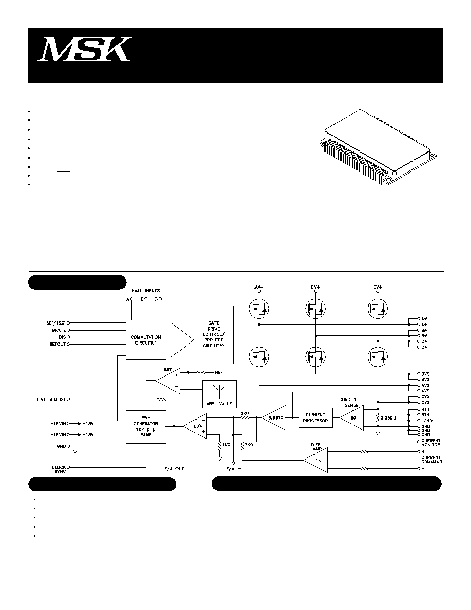
BLOCK DIAGRAM
DESCRIPTION:
The MSK 4324 is a complete 3 Phase MOSFET Bridge Brushless Motor Control System in a convenient isolated base-
plate package. The hybrid is capable of 10 amps of output current and 200 volts of DC bus voltage. It has the normal
features for protecting the bridge. Included is all the bridge drive circuitry, hall sensing circuitry, commutation circuitry and
all the current sensing and analog circuitry necessary for closed loop current mode (torque) control. When PWM'ing, the
transistors are modulated in locked anti-phase (complementary) mode for the tightest control and the most bandwidth.
Provisions for applying different compensation schemes are included. The MSK 4324 has good thermal conductivity of the
MOSFET's due to a hermetic isolated package design that allows direct heat sinking of the hybrid without insulators.
FEATURES:
PRELIMINARY Rev. - 2/06
TYPICAL APPLICATIONS
3 Phase Brushless DC Motor Control
Servo Control
Fin Actuator Control
Gimbal Control
AZ-EL Control
PIN-OUT INFORMATION
MIL-PRF-38534 CERTIFIED
1
2
3
4
5
6
7
8
9
10
11
REFOUT
HALL A
HALL B
HALL C
60/120
BRAKE
CLOCK SYNC
DIS
GND
NC
NC
12
13
14
15
16
17
18
19
20
21
22
E/A OUT
E/A-
GND
+CURRENT COMMAND
-CURRENT COMMAND
+15 VIN
CURRENT MONITOR
-15 VIN
NC
NC
ILIMIT ADJUST
23
24
25
26
27
28
29
30
31
32
33
GND
NC
NC
LGND
RTN
RTN
CVS
CVS
Cÿ
Cÿ
CV+
34
35
36
37
38
39
40
41
42
43
BVS
BVS
Bÿ
Bÿ
BV+
AVS
AVS
Aÿ
Aÿ
AV+

1
Free Running
@ 15mA Load
Current Command=0 Volts
@ 5mA Load
@ 5mA Load
Pin 22 1.92K
to GND
Whole Bridge
All Switches off, 100V,150∞C
@ 5 Amps, 150∞C Junction
Guaranteed by design but not tested. Typical parameters are representative of actual device performance but are for reference only.
Industrial grade and "E" suffix devices shall be tested to subgroups 1 and 4 unless otherwise specified.
Military grade devices ("H" suffix) shall be 100% tested to subgroups 1,2,3 and 4.
Subgroups 5 and 6 testing available upon request.
Subgroup 1,4 T
A
=T
C
=+25∞C
2,5 T
A
=T
C
=+125∞C
3,6 T
A
=T
C
=-55∞C
Measurements do not include offset current at 0V current command.
Continuous operation at or above absolute maximum ratings may adversly effect the device performance and/or life cycle.
This is to be used for MOSET thermal calculations only.
INPUT CURRENT
+15 VIN
-15 VIN
PWM Clock Frequency
CLOCK SYNC INPUT
VIL
VIH
Duty Cycle
Sync Frequency
LOGIC INPUTS (Hall A,B,C,Brake,60∞/120∞,DIS)
VIL
VIH
REFERENCE
ANALOG SECTION
Current Command Input Range
Current Command Input Current
Transconductance
Offset Current
Current Monitor
Current Motor Voltage Swing
Error Amp
E/A OUT Voltage Swing
Slew Rate
Gain Bandwidth Product
Large Signal Voltage Swing
Current Limit Adjust
OUTPUT SECTION
Voltage Drop Across Bridge
(1 Upper & 1 Lower)
Leakage Current
trr
Dead Time
Drain-Source On Resistance
High Voltage Supply
Current Command Input
Logic Inputs
REFOUT External Load
E/A OUT External Load
Clock SYNC Input
Continuous Output Current
Continuous Output Current @ 125∞C Case
Peak Output Current
200V
±13.5V
-0.2V to REFOUT
15 mA
5 mA
-0.2V to +15V
10 Amps
5 Amps
15 Amps
2
ELECTRICAL SPECIFICATIONS
ABSOLUTE MAXIMUM RATINGS
0.5∞C/W
-65∞C to +150∞C
+300∞C
-40∞C to +85∞C
-55∞C to +125∞C
+150∞C
R
JC
T
ST
T
LD
T
C
T
J
Parameter
Units
MSK 4324H/E
Test Conditions
mA
mA
mA
mA
mA
mA
KHz
KHz
V
V
%
KHz
V
V
V
V
mA
A/V
A/V
mA
V/A
V/A
V
V
V/µsec
MHz
V/mV
Amps
V
V
mA
nsec
µsec
Min.
Typ.
Max.
-
-
-
-
-
-
14
14
-
12.5
10
Clock+0
-
3.0
5.82
-13.5
-
0.90
0.85
-25
0.90
0.85
-12
-12
6.8
-
175
4
-
-
-
-
-
-
89
83
106
24
26
23
17
17
-
-
-
-
-
-
6.25
-
-
1.0
1.0
0
1.0
1.0
-
-
8
6.5
275
5
-
-
-
220
3
-
150
150
150
60
60
60
20
20
2.5
-
90
Clock+3
0.8
-
6.57
+13.5
1.5
1.1
1.15
+25
1.1
1.15
+12
+12
-
-
-
6
TBD
TBD
1
330
-
0.151
1
2
3
4
5
6
7
8
NOTES:
MSK 4324
Min.
Typ.
Max.
-
-
-
-
-
-
14
-
-
12.5
10
Clock+0
-
3.0
5.82
-13.5
-
0.85
-
-50
0.85
-
-12
-12
6.8
-
175
4
-
-
-
-
-
-
89
-
-
24
-
-
17
-
-
-
-
-
-
-
6.25
-
-
1.0
-
0
1.0
-
-
-
8
6.5
275
5
-
-
-
220
3
-
150
-
-
60
-
-
20
-
2.5
-
90
Clock+3
0.8
-
6.57
+13.5
1.5
1.15
-
+50
1.15
-
+12
+12
-
-
-
6
TBD
-
1
330
-
0.151
1
2
3
1
2
3
4
5,6
-
-
-
-
-
-
1
-
-
4
5,6
1
4
5,6
-
-
-
-
-
1
-
-
-
-
-
-
Group A
Subgroup
Output PWM'ing
Current Command=0 Volts
Output PWM'ing
Current Command=0 Volts
1
1
1
1
1
1
1
1
6
6
1
1
1
1
1
1
1
5
2
5
4
7
PRELIMINARY Rev. - 2/06
Thermal Resistance (Output Switches@125∞C)
Storage Temperature Range
Lead Temperature Range
(10 Seconds)
Case Operating Temperature
(MSK 4324)
(MSK 4324H/E)
Junction Temperature
5 Amps @ 125∞C T
C
1 8

APPLICATION NOTES
IN
MSK 4324 PIN DESCRIPTIONS
AV+, BV+, CV+ - are the power connections from the hy-
brid to the bus. The pins for each phase are brought out
separately and must be connected together to the V+ source
externally. The external wiring to these pins should be sized
according to the RMS current required by the motor. These
pins should be bypassed by a high quality monolithic ceramic
capacitor for high frequencies and enough bulk capacitance
for keeping the V+ supply from drooping.
Note: this is a power sequence sensitive part. Either turn on all
supplies simultaneously or provide ±15V first, then V+ voltages.
Aÿ, Bÿ & Cÿ- are the connections to the motor phase wind-
ings from the bridge output. The wiring to these pins should
be sized according to the current required by the motor. There
are no short circuit provisions for these outputs. Shorts to
V+ or ground from these pins must be avoided or the bridge
will be destroyed.
AVS, BVS, CVS - are the return pins on the bottom of each
half bridge. They are brought out separately and should be
connected together externally to allow the current from each
half bridge to flow through the sense resistor. The wiring on
these pins should be sized according to the current require-
ments of the motor.
RTN - is the power return connection from the module to the
bus. All ground returns connect to this point from internal to
the module in a star fashion. All external ground connections
to this point should also be made in a similar fashion. The
V+ capacitors should be returned to this pin as close as
possible. Wire sizing to this pin connection should be made
according to the required current.
LGND - is an isolated ground connection to the RTN pin of
the hybrid that is connected internally. For any circuitry that
needs to be connected to the RTN pin without the influence
of current flow through RTN should be connected at this
point.
GND - is a ground pin that connects to the ground plane for
all low powered circuitry inside the hybrid.
+15 VIN - is the input for applying +15 volts to run the low
power section of the hybrid. This pin should be bypassed
with a 10 µF capacitor and a 0.1 µF capacitor as close to this
pin as possible.
Note: this is a power sequence sensitive part. Either turn on all
supplies simultaneously or provide ±15V first, then V+ voltages.
-15 VIN - is the input for applying -15 volts to run the low
power section of the hybrid. This pin should be bypassed
with a 10 µF capacitor and a 0.1 µF capacitor as close to this
pin as possible.
Note: this is a power sequence sensitive part. Either turn on all
supplies simultaneously or provide ±15V first, then V+ voltages.
CURRENT COMMAND (+,-) - are differential inputs for con-
trolling the module in current mode. Scaled at ±1 amp per
volt of input command, the bipolar input allows both forward
and reverse current control capability regardless of motor com-
mutation direction. The maximum operational command volt-
age should be ±10 volts for ±10 amps of motor current.
3
CURRENT MONITOR - is a pin providing a current viewing
signal for external monitoring purposes. This is scaled at ±1
amp of motor current per volt output, up to a maximum of
±10 volts, or ±10 amps. As ±10 amps is exceeded, the
peaks of the waveform may become clipped as the rails of the
amplifiers are reached. This voltage is typically ±12.5 volts,
equating to ±12.5 amps of current peaks.
E/A OUT - is the current loop error amp output connection. It
is brought out for allowing various loop compensation circuits
to be connected between this and E/A-.
E/A- -is the current loop error amp inverting input connec-
tion. It is brought out for allowing various loop compensa-
tion circuits to be connected between this and E/A OUT.
CLOCK SYNC- is an input for synchronizing to an external
clock. The sync circuit will trigger on the edges of the ap-
plied clock and effectively shorten the period of the internal
oscillator on each cycle. The frequency can be increased
from a free running 14 KHz to 20 KHz maximum. The clock
applied shall be 15 volts amplitude with at least a 10% duty
cycle.
REFOUT - is a 6.25 volt regulated output to be used for pow-
ering the hall devices in various motors. Up to 15 mA of
output current is available.
HALL A, B & C - are the hall input pins from the hall devices
in the motor. These pins are internally pulled up to 6.25
volts. The halls can reflect a 120/240 degree commutation
scheme or a 60/300 degree scheme.
BRAKE - is a pin for commanding the output bridge into a
motor BRAKE mode. When pulled low, normal operation com-
mences. When pulled high, the 3 high side bridge switches
turn off and the 3 low side bridge switches turn on, causing
rapid deceleration of the motor and will cease motor opera-
tion until pulled high again. Logic levels for this input are TTL
compatible. It is necessary to toggle ON and OFF BRAKE
after power up before normal operation can begin. This is
necessary because of the bootstrap high-side power supplies
for each phase. These are not continuous high-side supplies
and need to be refreshed by turning on the low side switches
momentarily with the BRAKE. It is internally pulled high.
DIS - is a pin for externally disabling the output bridge. A
15V CMOS logic low will enable the bridge and a 15V CMOS
logic high will disable it. After using the DIS pin, the BRAKE
must be cycled ON and OFF before normal operation will be-
gin. This is due to the bootstrap high-side supplies needing
refreshing.
60/120- is a pin fpr selecting the orientation of the commuta-
tion sheme of the motor. A high state will produce 60/300
degree commutation, whereas a low state will produce 120/
240 degree commutation. Logic levels for this input are TTL
compatible. It is internally pulled high.
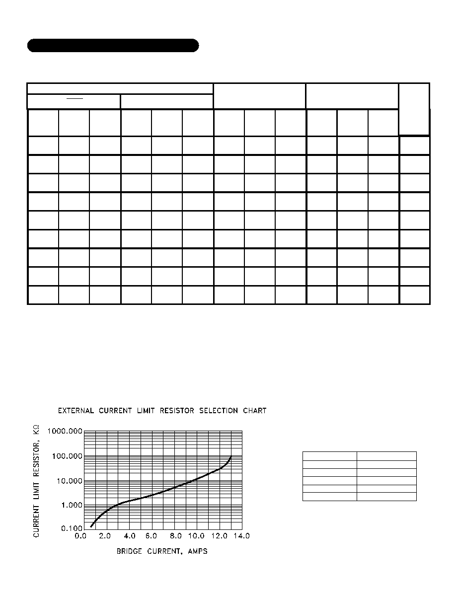
ILIMIT ADJUST - is a pin for externally adjusting the current
limit point. By placing a resistor to ground from this pin, a
voltage divider is created and the current limit will be lowered.
Without an external resistor, the current limit is set at 13 Amps.
PRELIMINARY Rev. - 2/06
HALL
A
HALL
B
HALL
C
HALL
A
HALL
B
HALL
C
Aÿ
Bÿ
Cÿ
Aÿ
Bÿ
Cÿ
1
0
0
1
0
0
H
-
L
L
-
H
0
1
1
0
1
1
0
-
H
L
-
L
H
0
0
1
0
1
1
1
L
H
-
H
L
-
0
0
1
1
0
1
1
L
-
H
H
-
L
0
0
0
1
0
0
1
-
L
H
-
H
L
0
1
0
1
0
0
0
H
L
-
L
H
-
0
1
1
1
1
0
1
-
-
-
-
-
-
0
0
0
0
0
1
0
-
-
-
-
-
-
0
X
X
X
X
X
X
L
L
L
L
L
L
1
4
1
=
High Level
H
=
SOURCE
NOTE:
Because of the true 4 quadrant method of output switching,
0
=
Low Level
L
=
SINK
the output switches will PWM between the I
COMMAND
POSITIVE
X
=
Don't Care
-
=
OPEN
and I
COMMAND
NEGATIVE states, with the average percentage
based on I
COMMAND
being a positive voltage and a negative
voltage. With a zero voltage I
COMMAND
, the output switches will
modulate with exactly a 50% duty cycle between the
I
COMMAND
POSITIVE and I
COMMAND
NEGATIVE states.
APPLICATION NOTES CONTINUED
COMMUTATION TRUTH TABLE
60∞
HALL SENSOR PHASING
120∞
I
COMMAND
= POS.
I
COMMAND
= NEG.
BRAKE
CURRENT (A)
2.0
4.0
6.0
8.0
10.0
RESISTOR (K
)
0.56
1.37
2.61
4.77
9.48
PRELIMINARY Rev. - 2/06
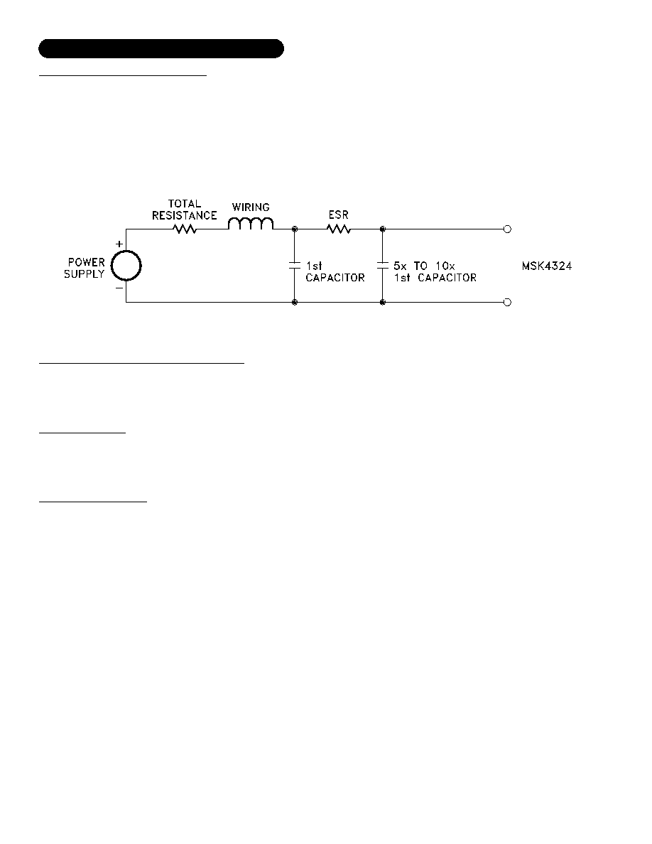
BUS VOLTAGE FILTER CAPACITORS
The size and placement of the capacitors for the DC bus has a direct bearing on the amount of noise filtered and also on the
size and duration of the voltage spikes seen by the bridge. What is being created is a series RLC tuned circuit with a resonant
frequency that is seen as a damped ringing every time one of the transistors switches. For the resistance, wire resistance,
power supply impedance and capacitor ESR all add up for the equivalent lumped resistance in the circuit. The inductance can
be figured at about 30 nH per inch from the power supply. Any voltage spikes are on top of the bus voltage and the back EMF
from the motor. All this must be taken into account when designing and laying out the system. If everything has been
minimized, there is another solution. A second capacitance between 5 and 10 times the first capacitor and it should either
have some ESR or a resistor can be added in series with the second capacitor to help damp the voltage spikes.
Be careful of the ripple current in all the capacitors. Excessive ripple current, beyond what the capacitors can handle, will
destroy the capacitors.
REGULATED VOLTAGE FILTER CAPACITORS
It is recommended that about 10 µF of capacitance (tantalum) for bypassing the + and -15V regulated outputs be placed as
close to the module pins as practical. Adding ceramic bypass capacitors of about 0.1 µF or 1 µF will aid in suppressing noise
transients.
GENERAL LAYOUT
Good PC layout techniques are a must. Ground planes for the analog circuitry must be used and should be tied back to the
small pin grounds 9, 14 and 23. Additional ground, pin 26 is an isolated ground that connects internally directly back to the
main DC bus ground pin 27, 28. This can be used as necessary for voltage sensing, etc.
LOW POWER STARTUP
When starting up a system utilizing the MSK 4324 for the first time, there are a few things to keep in mind. First, because of
the small size of the module, short circuiting the output phases either to ground or the DC bus will destroy the bridge. The
current limiting and control only works for current actually flowing through the bridge. The current sense resistor has to see the
current in order for the electronics to control it. If possible, for startup use a lower voltage and lower current power supply to
test out connections and the low current stability. With a limited current supply, even if the controller locks up, the dissipation
will be limited. By observing the E/A OUT pin which is the error amp output, much can be found out about the health and
stability of the system. An even waveform with some rounded triangle wave should be observed. As current goes up, the DC
component of the waveform should move up or down. At full current (with a regular supply) the waveform should not exceed
+8 volts positive peak, or -8 volts negative peak. Some audible noise will be heard which will be the commutation frequency.
If the motor squeals, there is instability and power should be removed immediately unless power dissipation isn't excessive due
to limited supply current. For compensation calculations, refer to the block diagram for all information to determine the amplifier
gain for loop gain calculations.
5
APPLICATION NOTES CONTINUED
PRELIMINARY Rev. - 2/06
6
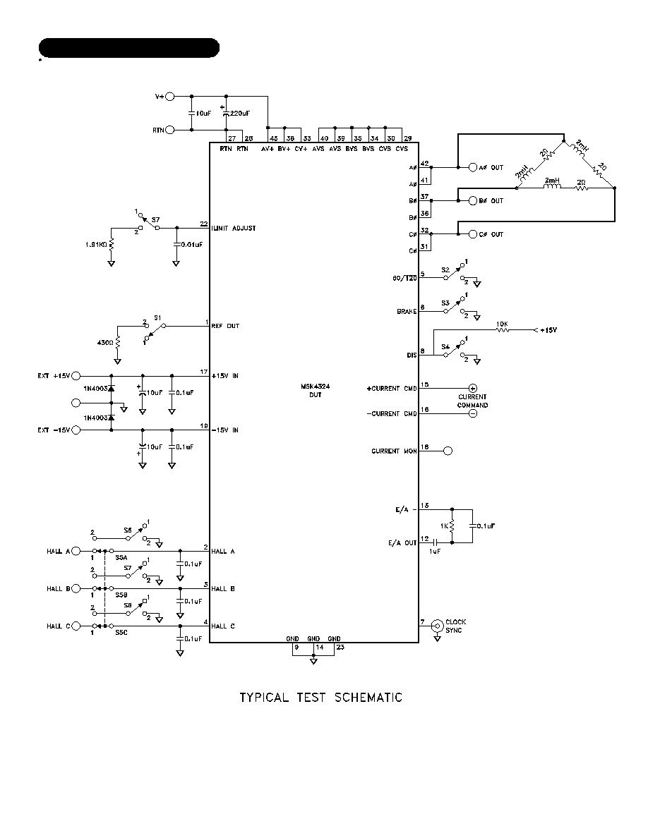
MSK4370 TEST CIRCUIT
PRELIMINARY Rev. - 2/06
7
The information contained herein is believed to be accurate at the time of printing. MSK reserves the right to make
changes to its products or specifications without notice, however, and assumes no liability for the use of its products.
Please visit our website for the most recent revision of this datasheet.
Contact MSK for MIL-PRF-38534 qualification status.
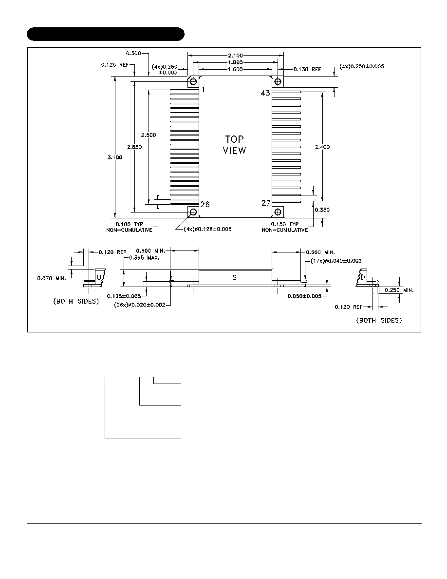
MECHANICAL SPECIFICATIONS
THE ABOVE EXAMPLE IS A MILITARY GRADE HYBRID WITH LEADS BENT UP.
M.S. Kennedy Corp.
4707 Dey Road, Liverpool, New York 13088
Tel. (315) 701-6751
FAX (315) 701-6752
www.mskennedy.com
MSK4324 H U
LEAD CONFIGURATION
S=STRAIGHT, U=BENT UP, D=BENT DOWN
ORDERING INFORMATION
NOTE: ALL DIMENSIONS ARE ±0.010 INCHES UNLESS OTHERWISE LABELED.
ESD TRIANGLE INDICATES PIN 1.
GENERAL PART NUMBER
SCREENING
BLANK=INDUSTRIAL; E=EXTENDED RELIABILITY;
H=MIL-PRF-38534 CLASS H
WEIGHT = 88 GRAMS TYPICAL
PRELIMINARY Rev. - 2/06