4707 Dey Road Liverpool, N.Y. 13088
M.S.KENNEDY CORP.
(315) 701-6751
FEATURES:
ISO-9001 CERTIFIED BY DSCC
Extremely Low Dropout Voltage 0.45V @ 10 Amps
Output Voltage Adjustable from +1.30V to +36V
Low External Component Count
Electrically Isolated Case
Low Quiescent Current
Output Current to 10 Amps
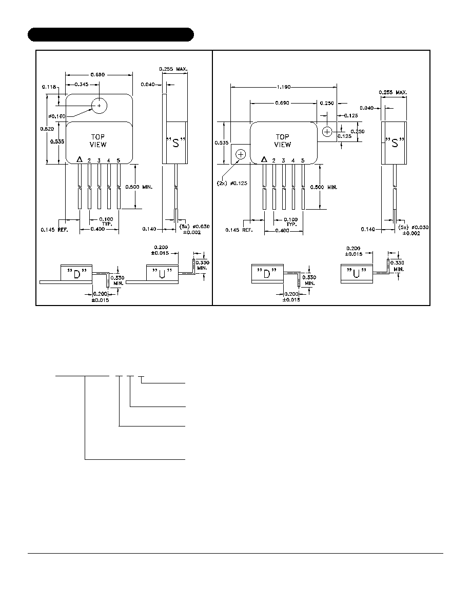
Available in Two Package Styles
Available with Three Lead Form Options
TYPICAL APPLICATIONS
High Efficiency, High Current Linear Regulators
Constant Voltage/Current Regulators
EQUIVALENT SCHEMATIC
5012
HIGH CURRENT,
SUPER LOW DROPOUT
ADJUSTABLE VOLTAGE REGULATOR
DESCRIPTION:
The MSK 5012 voltage regulator output is fully programmable through the use of two external resistors. Ultra low
dropout voltage specifications are realized due to the unique output configuration which uses an extremely low
Rds(on) MOSFET as a pass element. Dropout voltages of 0.45V at ten amps are typical in this configuration which
drives efficiency up and power dissipation down. Accuracy is guaranteed with a ±1% initial output voltage tolerance
that only varies ±2% with temperature. The MSK 5012 is packaged in a space efficient 5 pin SIP package that is
electrically isolated from the internal circuitry allowing direct heat sinking for efficient thermal dissipation.
MIL-PRF-38534 QUALIFIED
1
Rev. H 10/02
System Power Supplies
Switching Power Supply Post Regulators
Output Voltage Range
Input Voltage
Dropout Voltage
Dropout Voltage 2
Ripple Rejection
Thermal Resistance
Output Settling Time
VAdjust Voltage
Max.
36
±1.0
±2.0
36
0.010
0.75
±1.0
±2.0
±1.0
±1.0
10
10
-
0.8
-
1.248
V
%
%
V
V
V
%
%
%
%
mA
mA
dB
∞C/W
µ
S
V
Storage Temperature Range
Lead Temperature Range
(10 Seconds)
Case Operating Temperature
MSK5012
MSK5012B/E
Group A
Subgroup
-
1
2,3
-
1
1
1
2,3
1
2,3
1
2,3
-
-
-
1
V
IN
I
OUT
T
J
Input Voltage
Output Current
Junction Temperature
36V
10A within SOA
+175∞C
T
ST
T
LD
T
C
ABSOLUTE MAXIMUM RATINGS
-65∞C to +150∞C
300∞C
-40∞C to +85∞C
-55∞C to +125∞C
1
2
3
4
5
6
7
NOTES:
Output decoupled to ground using 47µF minimum capacitor and R1=30K
; R2=10K
unless otherwise specified.
This parameter is guaranteed by design but need not be tested. Typical parameters are representative of actual device
performance at 25∞C but are for reference only.
All output parameters are tested using a low duty cycle pulse to maintain T
J
= T
C
.
Industrial grade and "E" suffix devices shall be tested to subgroup 1 unless otherwise specified.
Military grade devices ('B' suffix) shall be 100% tested to subgroups 1,2 and 3.
Subgroup 1
Subgroup 2
Subgroup 3
Does not include tolerance effects from external resistors.
T
A
=T
C
=+25∞C
T
A
=T
C
=+125∞C
T
A
=T
C
=-55∞C
R2=10K
With Respect to V
OUT
I
OUT
= 0
A
I
OUT
=10A
V
IN
=V
OUT
+3V
100mA
I
OUT
9A
f=120Hz
Junction to Case @ 125∞C
To within 10mV (I
OUT
=0A)
V
IN
= V
OUT
+3V
Max.
36
±1.5
-
36
0.010
1.0
±1.5
-
±1.5
-
12
-
-
0.8
-
1.26
Parameter
MSK 5012
MSK 5012B/E
ELECTRICAL SPECIFICATIONS
Min.
1.3
-
-
1.3
-
-
-
-
-
-
-
-
-
-
-
1.222
Typ.
-
±0.3
±1.0
-
0.002
0.4
±0.5
±0.5
±0.3
-
4.5
-
45
0.7
5
1.235
Min.
1.3
-
1.3
-
-
-
-
-
-
-
-
-
-
-
1.21
Typ.
-
±0.3
-
-
0.002
0.5
±0.5
-
±0.3
-
4.5
-
45
0.7
5
1.24
2
3
Test Conditions
Load Regulation
(V
OUT
+1.5)
V
IN
(V
OUT
+15), I
OUT
=100mA
Units
Line Regulation
2
2
Rev. H 10/02
V
IN
=V
OUT
+3V; I
OUT
=0A
Quiescent Current
I
OUT
=100mA; V
IN
=V
OUT
+3V
Ouput Voltage Tolerance
7
2
2
2
APPLICATION NOTES
MINIMIZING OUTPUT RIPPLE:
The output voltage ripple of the MSK 5012 voltage regulator
can be minimized by placing a filter capacitor from the output
to ground. The optimum value for this capacitor may vary
from one application to the next and is best determined by
experimentation. Transient load response can also be improved
by placing a capacitor directly across the load. Typically a
10µF capacitor is a good starting point.
CASE CONNECTIONS:
The case of the MSK 5012 is electrically isolated from the
internal circuitry so that a direct connection can be made to
the heat sink for most efficient heat dissipation. However, it
may be necessary in some applications to connect the case to
ground. Grounding the case will help eliminate oscillations and
produce a clean, noise free output.
LOAD REGULATION:
For best results, the ground pin should be connected directly to
the load (see next note). This effectively reduces the ground
loop effect and eliminates excessive voltage drop in the sense
leg. It is also important to keep the output connection be-
tween the regulator and the load as short as possible since this
directly affects the load regulation. For example, if 20 gauge
wire were used which has a resistance of about .008 ohms per
foot, this would result in a drop of 8mV/ft at a load current of
1 amp.
LOAD CONNECTIONS:
In voltage regulator applications where very large load cur-
rents are present, the load connection is very important. The
path connecting the output of the regulator to the load must be
extremely low impedance to avoid affecting the load regulation
specifications. Any impedance in this path will form a voltage
divider with the load. The same holds true for the connection
from the low end of the load to ground. For best load regula-
tion, the low end of the load must be connected directly to pin
2 of the MSK 5012 and not to a ground plane inches away
from the hybrid.
FILTER CAPACITOR:
For all applications, the user must connect a 1.0uF capacitor
from pin 5 directly to ground. This capacitor is part of the
circuit which drives the gate of the internal MOSFET. Approxi-
mately three times the voltage seen on the input will appear
across this capacitor. Careful attention must be paid to capaci-
tor voltage rating since voltages larger than the power supply
are present.
First, the power dissipation must be calculated as follows:
Power Dissipation = (Vin - Vout) x Iout
Next, the user must select a maximum junction temperature.
The absolute maximum allowable junction temperature is 175∞C.
The equation may now be rearranged to solve for the required
heat sink to ambient thermal resistance (R
sa).
EXAMPLE:
An MSK 5012 is configured for Vin = +7V and Vout = +3.3V.
Iout is a continuous 10A DC level. The ambient temperature is
+25∞C. The maximum desired junction temperature is 150∞C.
R
jc = 0.8∞C/W and R
cs = 0.15∞C/W typically.
Power Dissipation = (7V - 3.3V) x (10A)
Solve for R
sa:
R
sa = 150∞C - 25∞C - 0.8∞C/W - 0.15∞C/W
In this example, a heat sink with a thermal resistance of no
more than 2.43∞C/W must be used to maintain a junction tem-
perature of no more than 150∞C. The Thermalloy Corporation
makes a heat sink with a thermal resistance of 2.2∞C/W that
would work well for this application.
(See Thermalloy part number 7023)
HEAT SINK SELECTION:
To select a heat sink for the MSK 5012, the following formula
for convective heat flow must be used.
Governing Equation:
Tj = Pd x (R
jc + R
cs + R
sa) + Ta
WHERE:
Tj = Junction Temperature
Pd = Total Power Dissipation
R
jc = Junction to Case Thermal Resistance
R
cs = Case to Heat Sink Thermal Resistance
R
sa = Heat Sink to Ambient Thermal Resistance
Ta = Ambient Temperature
37W
POWER DISSIPATION:
The output pass transistor in the MSK 5012 is rated to dissi-
pate nearly 100 watts. The limiting factor of this device is
effective dissipation of heat generated under such conditions.
For example, to dissipate 100 watts, calculations show that
the MSK 5012 would have to be bolted to the underbelly of a
submarine submerged in the Arctic Ocean! Careful consider-
ation must be paid to heat dissipation and junction temperature
when applying this device.
= 37 Watts
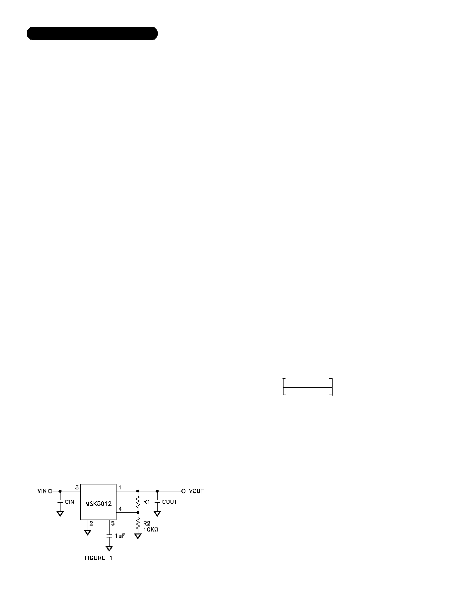
OUTPUT VOLTAGE ADJUSTMENT
The output voltage of the MSK 5012 can be adjusted from
+1.3 volts to +36 volts. Refer to the following formula for
resistor divider selection. R2 should be 10K
for all applica-
tions.
R1 = R2 ((V
OUT
/ 1.235) -1)
Figure one below illustrates proper resistor divider connection.
3
Rev. H 10/02