4707 Dey Road Liverpool, N.Y. 13088
M.S.KENNEDY CORP.
(315) 701-6751
FEATURES:
5041
SERIES
HIGH EFFICIENCY,
8 AMP 1% ACCURATE
SURFACE MOUNT
SWITCHING REGULATORS
Up To 95% Efficiency For 5V Version
8 Amp Output Current
4.5V to 30V Input Range
Preset 1.9V, 2.5V, 3.3V or 5.0V Output Versions
300KHz Switching Frequency @ 1 Amp and above
User Programmable Soft-Start
Quiescent Current < 2.5mA
User Programmable Current Limit
Available with Gull Wing Leads
Contact MSK for MIL-PRF-38534 Qualification Status
DESCRIPTION:
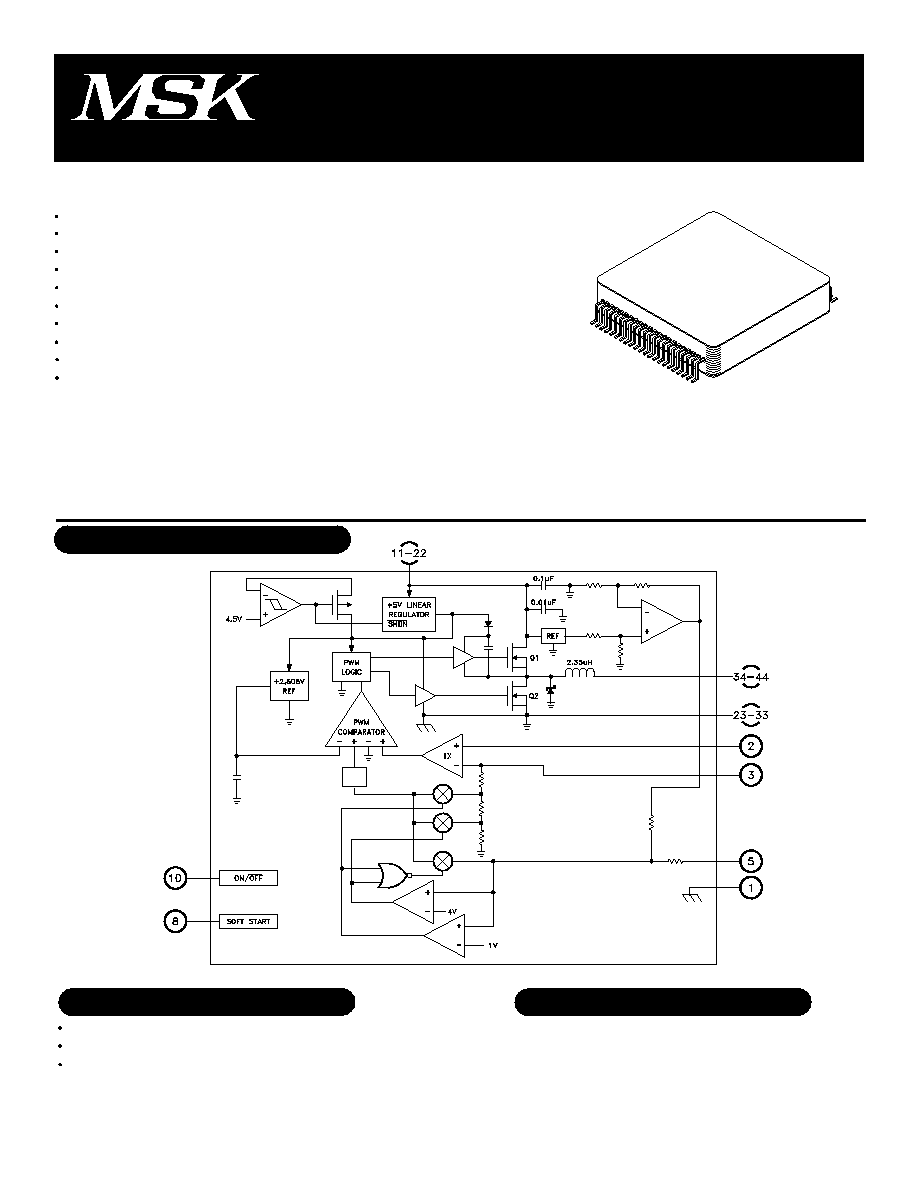
EQUIVALENT SCHEMATIC
The MSK 5041 series are high efficiency, 8 amp, surface mount switching regulators. The output voltage is
configured for 1.9V, 2.5V, 3.3V or 5.0V internally with a tolerance of 1% at 3 amps. The operating frequency of the
MSK 5041 is 300KHz and is internally set. An external "soft start" capacitor allows the user to control how quickly
the output comes up to regulation voltage after the application of an input. An extremely low quiescent current of
typically less than 2.5mA and nearly 95% operating efficiency keep the total internal power dissipation of the MSK
5041 down to an absolute minimum.
MIL-PRF-38534 CERTIFIED
TYPICAL APPLICATIONS
PIN-OUT INFORMATION
Step-down Switching Regulator
Microprocessor Power Source
High Efficiency Low Voltage
Subsystem Power Supply
Case
Sense High
Sense Low
N/C
RF High
N/C
N/C
1
2
3
4
5
6
7
34-44
23-33
11-22
10
9
8
Vout
Ground
Vin
Enable
N/C
Cton
Rev. B 2/06
1

Within SOA
1.0A
I
OUT
4.5A
I
OUT
=3.0A 6V
V
IN
20V
Internal I
OUT
1.5A
High
Low
V
EN
=V
IN
V
EN
=0V
V
EN
=0V V
IN
=30V
Positive
Negative
Source
Fault Sink
V
IN
=5.0V I
OUT
=3.0A
V
IN
=5.0V I
OUT
=3.0A
V
IN
=5.0V I
OUT
=3.0A
V
IN
=6V I
OUT
=3.0A
Enable Input Voltage
Enable Input Current
Current Limit Threshold
Cton Current
Efficiency
8
5041-1.9
5041-2.5
5041-3.3
5041-5.0
V
V
V
V
V
V
V
V
V
A
%
%/V
KHz
V
V
µA
µA
mA
mV
mV
µA
mA
%
%
%
%
T
ST
T
LD
T
C
T
J
Storage Temperature Range
Lead Temperature Range
(10 Seconds)
Case Operating Temperature
MSK5041 Series
MSK5041H/E Series
Junction Temperature
ABSOLUTE MAXIMUM RATINGS
-65∞C to +150∞C
300∞C
-40∞C to +85∞C
-55∞C to +125∞C
+150∞C
Input Voltage
Enable Voltage
Output Current
Sense Pin Voltage
Thermal Resistance
(Each MOSFET)
-0.3V, +36V
-0.3V, +36V
9.0 Amps
-0.3V, +7V
12∞C/W
1,2,3
1
2,3
1
2,3
1
2,3
1
2,3
1
-
1,2,3
-
1,2,3
1,2,3
1
1
1
1
1
1
1
1
1
1
1
Input Supply Range
Output Current
Load Regulation
Line Regulation
Oscillator Frequency
Disabled Quiescent Current
-
1.9
-
2.5
-
3.3
-
5.0
-
9.0
2.5
0.06
300
-
-
0.5
0.2
2.0
100
-100
4.0
-
70
80
90
95
ELECTRICAL SPECIFICATIONS
4.75
1.88
1.8
2.47
2.38
3.27
3.14
4.95
4.75
8.0
-
-
270
2.0
-
-
-
-
80
-50
2.5
2.0
-
-
-
-
-
1.9
1.9
2.5
2.5
3.3
3.3
5.0
5.0
9.0
2.5
0.06
300
-
-
0.5
0.2
2.0
100
-100
4.0
-
70
80
90
95
30
1.92
2.0
2.53
2.63
3.33
3.47
5.05
5.25
-
-
0.10
330
-
0.5
2.0
2.0
2.5
120
-160
6.5
-
-
-
-
-
4.75
1.86
-
2.45
-
3.23
-
4.9
-
8.0
-
-
270
2.0
-
-
-
-
75
-45
2.5
2.0
-
-
-
-
30
1.94
-
2.55
-
3.37
-
5.1
-
-
-
0.12
330
-
0.5
2.0
2.0
2.5
125
-165
6.5
-
-
-
-
-
Group A
Subgroup
Min.
Typ.
Max.
Min.
Typ.
Max.
MSK 5041 SERIES
MSK 5041H SERIES
Units
Test Conditions
Parameter
1
2
2
2
2
2
2
2 7
1
2
3
4
5
6
7
8
9
V
IN
=Enable, 5mV
(sense high-sense low)
25mV, I
L
=0A, C
OUT
=10x330µF, C
IN
=10x220µF, C
TON
=0.01µF unless otherwise specified.
This parameter is guaranteed by design but need not be tested. Typical parameters are representative of actual device performance but are for reference only.
All output parameters are tested using a low duty cycle pulse to maintain T
J
= T
C
.
Industrial grade and 'E' suffix devices shall be tested to subgroup 1 unless otherwise specified.
Military grade devices ('H' suffix) shall be 100% tested to subgroups 1,2 and 3.
Subgroup 1
Subgroup 2
Subgroup 3
Actual switching frequency can be load dependent if output current is low. Refer to typical performance curves.
Alternate output voltages are available. Please contact the factory.
Continuous operation at or above absolute maximum ratings may adversely effect the device performance and/or life cycle.
T
A
=T
C
=+25∞C
T
A
=T
C
=+125∞C
T
A
=T
C
=-55∞C
NOTES:
2
8
2
8
8
Output Voltage 5041-1.9
Output Voltage 5041-2.5
Output Voltage 5041-3.3
Output Voltage 5041-5.0
I
OUT
=3.0A V
IN
=5.0V
I
OUT
=3.0A V
IN
=5.0V
I
OUT
=3.0A V
IN
=5.0V
I
OUT
=3.0A V
IN
=6V
Rev. B 2/06
9
The output capacitor values are generally determined by
the ESR and voltage rating requirements rather than capaci-
tance requirements for stability. Low ESR capacitors that meet
the ESR requirement usually have more output capacitance than
required for stability. Only specialized low-ESR capacitors in-
tended for switching-regulator applications, such as AVX TPS,
Sprague 595D, Sanyo OS-CON, Nichicon PL series or Kemet
T510 series should be used. The capacitor must meet mini-
mum capacitance and maximum ESR values as given in the
following equations:
C
F
> 2.5V(1 + V
OUT
/V
IN(MIN)
)
V
OUT
x R
SENSE
x f
R
ESR
< R
SENSE
x V
OUT
2.5V
APPLICATION NOTES
CURRENT LIMITING:
The MSK 5041 is equipped with a pair of sense pins that
are used to sense the load current using an external resistor
(Rs). The current-limit circuit resets the main PWM latch and
turns off the internal high-side MOSFET switch whenever the
voltage difference between Sense High and Sense Low ex-
ceeds 100mV. This limiting occurs in both current flow direc-
tions, putting the threshold limit at ±100mV. The tolerance
on the positive current limit is ±20%. The external low-value
sense resistor must be sized for 80mV/Rs to guarantee enough
load capacity. Load components must be designed to with-
stand continuous current stresses of 120mV/Rs.
For very high-current applications, it may be useful to wire
the sense inputs with a twisted pair instead of PCB traces.
This twisted pair needn't be anything unique, perhaps two pieces
of wire-wrap wire twisted together. Low inductance current
sense resistors, such as metal film surface mount styles are
best.
SOFT START/Cton:
The internal soft-start circuitry allows a gradual increase of
the internal current-limit level at start-up for the purpose of
reducing input surge currents, and possibly for power-supply
sequencing. In Disable mode, the soft-start circuit holds the
Cton capacitor discharged to ground. When Enable goes high,
a 4µA current source charges the Cton capacitor up to 3.2V.
The resulting linear ramp causes the internal current-limit thresh-
old to increase proportionally from 20mV to 100mV. The out-
put capacitors charge up relatively slowly, depending on the
Cton capacitor value. The exact time of the output rise de-
pends on output capacitance and load current and is typically
1mS per nanofarad of soft-start capacitance. With no capaci-
tor connected, maximum current limit is reached typically within
10µS.
ENABLE FUNCTION:
The MSK 5041 is enabled by applying a logic level high to
the Enable pin. A logic level low will disable the device and
quiescent input current will reduce to approximately 2mA. The
Enable threshold voltage is 1V. If automatic start up is re-
quired, simply connect the pin to V
IN
. Maximum Enable volt-
age is +36V.
INPUT CAPACITOR SELECTION:
OUTPUT CAPACITOR SELECTION:
These equations provide 45 degrees of phase margin to
ensure jitter-free fixed-frequency operation and provide a damped
output response for zero to full-load step changes. Lower qual-
ity capacitors can be used if the load lacks large step changes.
Bench testing over temperature is recommended to verify ac-
ceptable noise and transient response. As phase margin is
reduced, the first symptom is timing jitter, which shows up in
the switching waveforms. Technically speaking, this typically
harmless jitter is unstable operation, since the switching fre-
quency is non-constant. As the capacitor ESR is increased,
the jitter becomes worse. Eventually, the load-transient wave-
form has enough ringing on it that the peak noise levels exceed
the output voltage tolerance. With zero phase margin and in-
stability present, the output voltage noise never gets much
worse than I
PEAK
x R
ESR
(under constant loads). Designers of
industrial temperature range digital systems can usually multi-
ply the calculated ESR value by a factor of 1.5 without hurting
stability or transient response.
The output ripple is usually dominated by the ESR of the
filter capacitors and can be approximated as I
RIPPLE
x R
ESR
.
Including the capacitive term, the full equation for ripple in the
continuous mode is V
NOISE(p-p)
=I
RIPPLE
x (R
ESR
+ 1/(2
fC)). In
idle mode, the inductor current becomes discontinuous with
high peaks and widely spaced pulses, so the noise can actually
be higher at light load compared to full load. In idle mode, the
output ripple can be calculated as follows:
V
NOISE(p-p)
= 0.02 x R
ESR
+ 0.0003 x 2.35µH x [1/V
OUT
+ 1/(V
IN
-V
OUT
)]
R
SENSE
(R
SENSE
)≤ x C
3
POWER DISSIPATION:
In high current applications, it is very important to ensure
that both MOSFETS are within their maximum junction tem-
perature at high ambient temperatures. Temperature rise can
be calculated based on package thermal resistance and worst
case dissipation for each MOSFET. These worst case dissipa-
tions occur at minimum voltage for the high side MOSFET and
at maximum voltage for the low side MOSFET.
Calculate power dissipation using the following formulas:
Pd (upper FET)=I
LOAD
≤ x 0.022
x DUTY
+ V
IN
x I
LOAD
x f x V
IN
x C
RSS
+20ns
I
GATE
Pd (lower FET)=I
LOAD
≤ x 0.022
x (1-DUTY)
DUTY= (V
OUT
+V
Q2
)
(V
IN
-V
Q1
)
Where: V
Q1
or V
Q2
(on state voltage drop)=I
LOAD
x 0.022
C
RSS
=94pF
I
GATE
=1A
During output short circuit, Q2, the synchronous-rectifier
MOSFET, will have an increased duty factor and will see addi-
tional stress. This can be calculated by:
Q2 DUTY=1- V
Q2
V
IN(MAX)
-V
Q1
Where: V
Q1
or V
Q2
=(120
MV
/R
SENSE
)x0.022
The MSK 5041 has an internal high frequency ceramic ca-
pacitor (0.1uF) between V
IN
and GND. Connect a low-ESR
bulk capacitor directly to the input pin of the MSK 5041. Se-
lect the bulk input filter capacitor according to input ripple-
current requirements and voltage rating, rather than capacitor
value. Electrolytic capacitors that have low enough ESR to
meet the ripple-current requirement invariably have more than
adequate capacitance values. Aluminum-electrolytic capaci-
tors are preferred over tantalum types, which could cause power-
up surge-current failure when connecting to robust AC adapt-
ers or low-impedance batteries. RMS input ripple current is
determined by the input voltage and load current, with the
worst possible case occuring at V
IN
= 2 x V
OUT
:
I
RMS
= I
LOAD
X
V
OUT
(V
IN
-V
OUT
)
V
IN
Rev. B 2/06
APPLICATION NOTES CONT'D
RF HIGH:
It is very important that the DC voltage returned to the RF high pin from the output be as noise and oscillation free as possible.
This voltage helps to determine the final output and therefore must be a clean voltage. Excessive noise or oscillation can cause the
device to have an incorrect output voltage. Proper PC board layout techniques can help to achieve a noise free voltage at the RF
high pin.
Under heavy loads, the MSK 5041 operates in full PWM mode. Each pulse from the oscillator sets the internal PWM latch that
turns on the high-side MOSFET. As the high-side switch turns off, the synchronous rectifier latch is set. 60ns later the low-side
MOSFET turns on until the start of the next clock cycle or until the inductor current crosses zero. Under fault conditions the current
exceeds the ±100mV current-limit threshold and the high-side switch turns off.
At light loads the inductor current does not exceed the 30mV threshold set by the minimum-current comparator. When this
occurs, the MSK 5041 goes into idle mode, skipping most of the oscillator pulses in order to reduce the switching frequency and
cut back gate-charge losses. The oscillator is gated off at light loads because the minimum-current comparator immediately resets
the high-side latch at the start of each cycle. Refer to Table 1 for the operational characteristics.
DEVICE DISABLED
PULSE SKIPPING MODE DISCONTINUOUS INDUCTOR CURRENT
PULSE SKIPPING MODE CONTINUOUS INDUCTOR CURRENT
CONSTANT FREQ. PWM MODE CONTINUOUS INDUCTOR CURRENT
DESCRIPTION
0
1
1
1
ENABLE
LOAD
X
LOW <10%
MED <30%
HIGH >30%
OPERATIONAL CHARACTERISTICS
TABLE 1
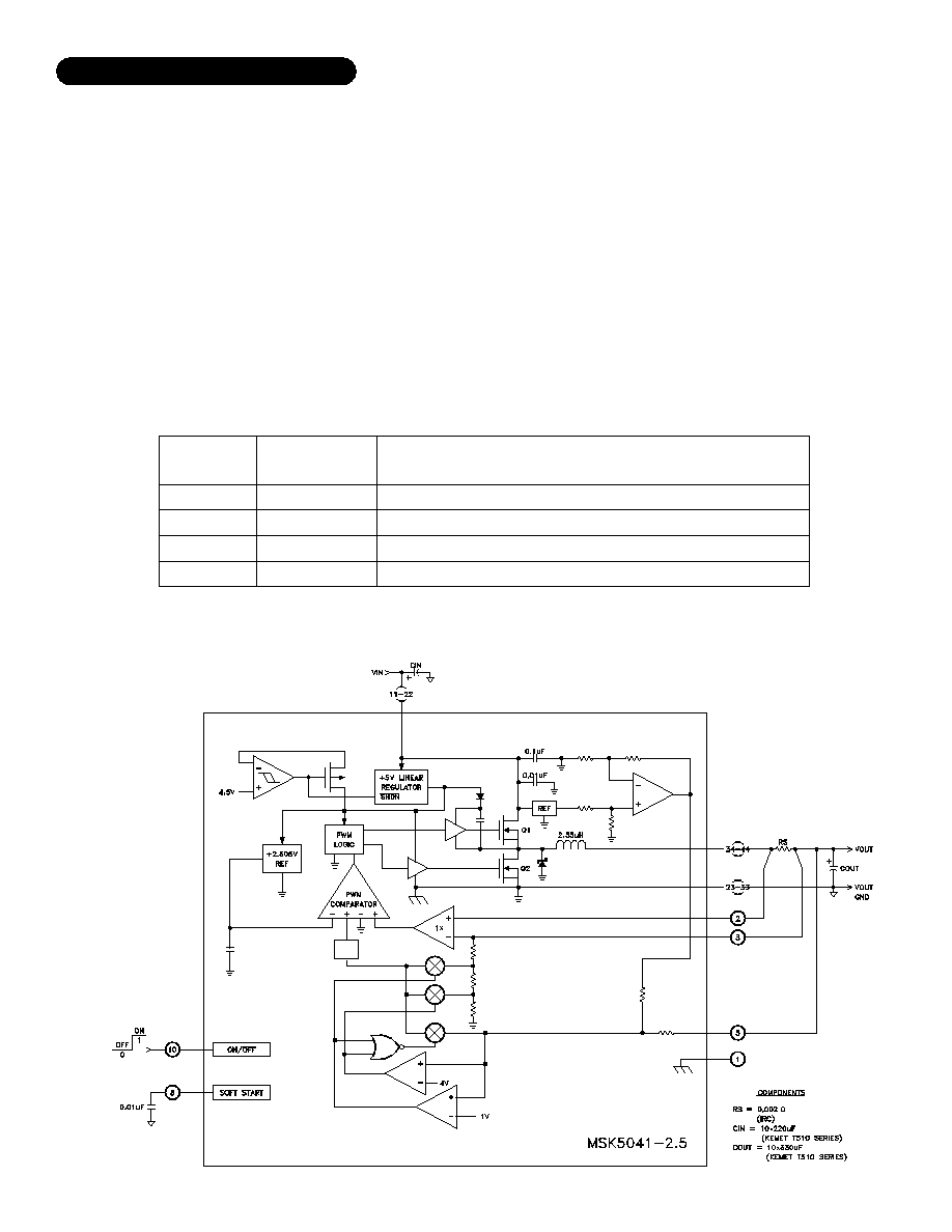
TYPICAL 2.5V APPLICATION CIRCUIT
4
MODES OF OPERATION:
Rev. B 2/06

TYPICAL PERFORMANCE CURVES
5
PERFORMANCE CURVES ARE CURRENTLY UNDER DEVELOPMENT
Rev. B 2/06

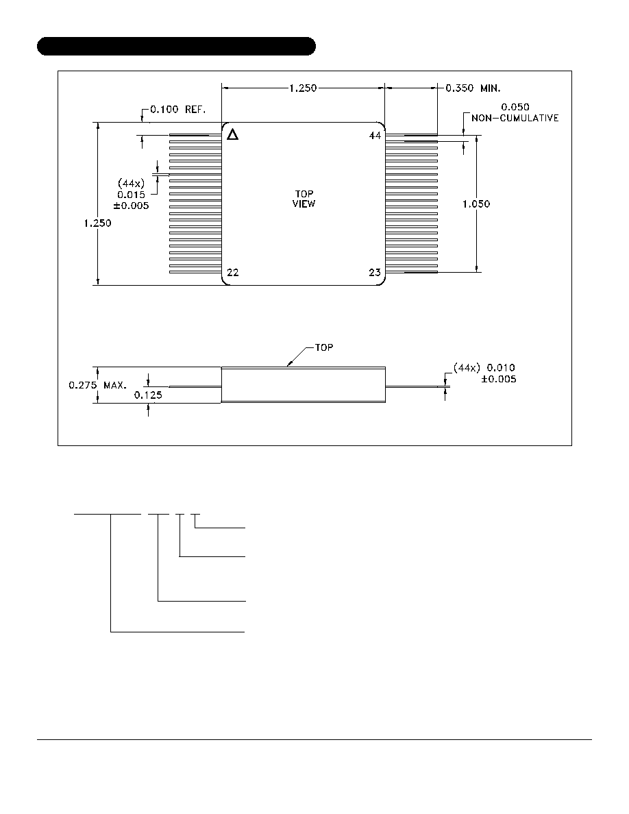
MECHANICAL SPECIFICATIONS
LEAD FORM OPTIONS
BLANK=STRAIGHT; G=GULL WING
SCREENING
BLANK=INDUSTRIAL; H=MIL-PRF-38534
E=EXTENDED RELIABILITY
OUTPUT VOLTAGE
1.9V=+1.9V; 2.5=+2.5V; 3.3=+3.3V; 5.0=+5.0V
GENERAL PART NUMBER
The above example is a +3.3V, MIL-PRF-38534 Class H regulator with gull wing leads.
WEIGHT=16 GRAMS TYPICAL
ESD Triangle indicates Pin 1
NOTE: ALL DIMENSIONS ARE ±0.010 INCHES UNLESS OTHERWISE LABELED.
MSK5041-3.3 H G
ORDERING INFORMATION
6
Rev. B 2/06
The information contained herein is believed to be accurate at the time of printing. MSK reserves the right to make
changes to its products or specifications without notice, however, and assumes no liability for the use of its products.
Please visit our website for the latest revision of this datasheet.
Contact MSK for MIL-PRF-38534 qualification status.
MECHANICAL SPECIFICATIONS CONTINUED
M.S. Kennedy Corp.
4707 Dey Road, Liverpool, New York 13088
Phone (315) 701-6751
FAX (315) 701-6752
www.mskennedy.com
LEAD FORM OPTIONS
BLANK=STRAIGHT; G=GULL WING
SCREENING
BLANK=INDUSTRIAL; H=MIL-PRF-38534
E=EXTENDED RELIABILITY
OUTPUT VOLTAGE
1.9V=+1.9V; 2.5=+2.5V; 3.3=+3.3V; 5.0=+5.0V
GENERAL PART NUMBER
The above example is a +3.3V, MIL-PRF-38534 Class H regulator.
WEIGHT=16 GRAMS TYPICAL
ESD Triangle indicates Pin 1
NOTE: ALL DIMENSIONS ARE ±0.010 INCHES UNLESS OTHERWISE LABELED.
MSK5041-3.3 H
ORDERING INFORMATION
7
Rev. B 2/06