The MSK 5046RH series are high efficiency, 5 amp, radiation hardened switching regulators. The output voltage is
configured for 1.5V,1.7V,1.8V,1.9V,2.0V,2.5V,3.0V,3.3V,3.4V or 5.0V internally with a tolerance of 1%. The very
low output impedance allows the MSK 5046RH to drive the start up surge current required by many CPU's and
FPGA's with little or no decrease in the output voltage. The operating frequency of the MSK 5046RH is 350KHz. A
low quiescent current and very good operating efficiency keep the total internal power dissipation of the MSK
5046RH down to an absolute minimum. The device is packaged in a hermetic surface mountable package for high
reliability applications.
4707 Dey Road Liverpool, N.Y. 13088
M.S.KENNEDY CORP.
(315) 701-6751
FEATURES:
5046RH
SERIES
RADIATION HARDENED
HIGH EFFICIENCY, 5 AMP
SWITCHING REGULATORS
Up To 92% Conversion Efficiency For 5V Version
5 Amp Output Current
3.1V to 18V Input Range with Separate Bias
12V to 18V Input Range with UVLO (VBIAS=VIN)
Preset 1.5V,1.7V,1.8V,1.9V,2.0V,2.5V,3.0V,3.3V,3.4V or 5.0V Output Versions
User Programmable Current Limit
Output Trim Capability
Custom Compensation & Outputs Available
350KHz Switching Frequency
Surface Mountable Hermetic Package
-55∞C to +125∞C Operating Temperature Range
Total Dose Tested to 300K RAD
Available with Gull Wing Leads
Contact MSK for MIL-PRF-38534 Qualification and Appendix G (Radiation Status)
DESCRIPTION:
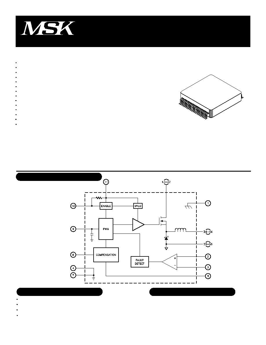
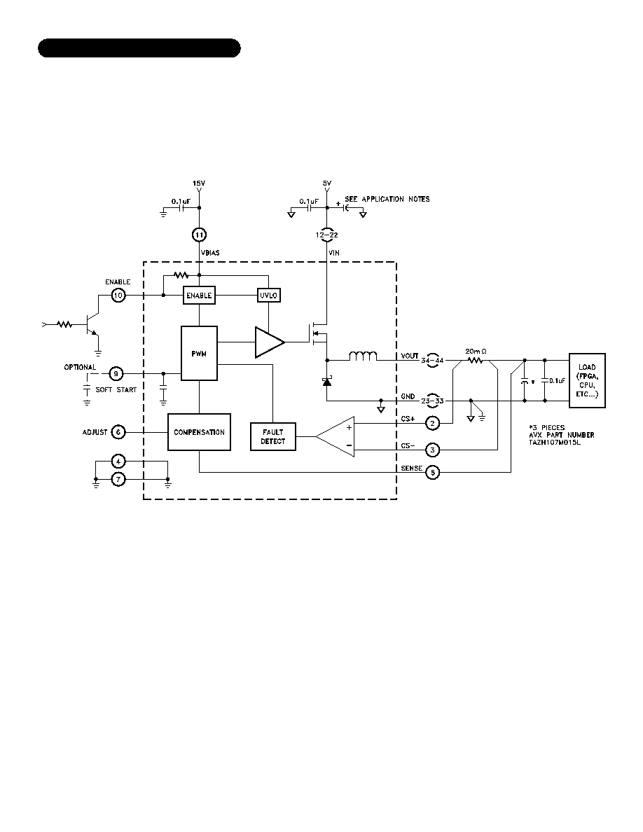
EQUIVALENT SCHEMATIC
MIL-PRF-38534 CERTIFIED
TYPICAL APPLICATIONS
PIN-OUT INFORMATION
Satellite System Power Supply
Step-down Switching Regulator
Microprocessor, FPGA Power Source
High Efficiency Low Voltage
Subsystem Power Supply
1
2
3
4
5
6
7
PRELIMINARY Rev. G 2/06
1
CASE
CS+
CS-
SIGNAL GROUND
SENSE
ADJUST
SIGNAL GROUND
8
9
10
11
12-22
23-33
34-44
NC
SOFT START
ENABLE
VBIAS
VIN
POWER GROUND
VOUT
-0.3V, +20V
-0.3V, 18V
-0.3V, VBIAS
5.0 Amps
6.0∞C/W
7.5∞C/W
T
ST
T
LD
T
C
T
J
Storage Temperature Range
Lead Temperature Range
(10 Seconds)
Case Operating Temperature
MSK5046RH K/H/E Series
MSK5046RH Series
Junction Temperature
ABSOLUTE MAXIMUM RATINGS
-65∞C to +150∞C
300∞C
-55∞C to +125∞C
-40∞C to +85∞C
+150∞C
Input Voltage
VBIAS Voltage
Enable
Output Current
Thermal Resistance MOSFET(@ 125∞C)
Diode(@ 125∞C)
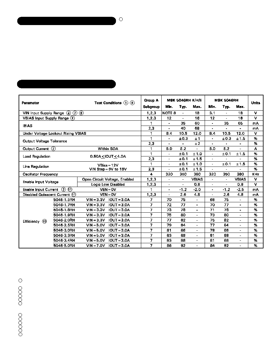
ELECTRICAL SPECIFICATIONS
PRELIMINARY Rev. G 2/06
2
NOTES:
1
2
3
4
5
6
7
8
9
10
11
12
VIN=12V, VBIAS=12V, I
OUT
=4.0A, R
SENSE
=15m
, C
OUT
=3x100µF Low ESR tantalum (AVX P/N TAZH107M015L) + 1.0µF ceramic,
SOFT START=NC, ENABLE=NC, ADJUST=NC, unless otherwise specified.
Guaranteed by design but not tested. Typical parameters are representative of actual device performance but are for reference only.
All output parameters are tested using a low duty cycle pulse to maintain T
J
= T
C
.
Industrial grade and 'E' suffix devices shall be tested to subgroup 1 unless otherwise specified.
Military grade devices ('H' and 'K' suffix) shall be 100% tested to subgroups 1,2,3,4 and 7.
Subgroup 1,4,7
Subgroup 2
Subgroup 3
The device can operate with input voltages as high as 18V, but efficiency is best at lower inputs.
With VBIAS connected to a separate source, VIN Min. is V
OUT
+ V
DROPOUT
; see typical dropout curves.
Contact factory for post radiation limits.
Sense resistor losses and VBIAS power not included. See typical performance curves.
The disabled bias current is the sum of the enable pin sink current (approximately VBIAS/10K
) and the internal bias current.
Continuous operation at or above absolute maximum ratings may adversely effect the device performance and/or life cycle.
T
A
=T
C
=+25∞C
T
A
=T
C
=+125∞C
T
A
=T
C
=-55∞C
12
APPLICATION NOTES
PRELIMINARY Rev. G 2/06
3
INPUT CAPACITOR SELECTION:
The MSK 5046RH should have an external high fre-
quency ceramic capacitor (0.1uF) between VIN and power
ground. Connect a low-ESR bulk capacitor directly to
the input pin of the MSK 5046RH. Select the bulk input
filter capacitor according to input ripple-current require-
ments and voltage rating, rather than capacitor value.
Electrolytic capacitors that have low enough ESR to meet
the ripple-current requirement invariably have more than
adequate capacitance values. Aluminum-electrolytic ca-
pacitors are preferred over tantalum types, which could
cause power-up surge-current failure when connecting
to robust AC adapters or low-impedance batteries.
INPUT BIAS AND UVLO:
The VBIAS pin of the MSK 5046RH provides bias to
the control circuitry. The VBIAS pin can be connected
directly to the input bus for 12V to 18V operation or it
can be biased separately with a 12V to 18V source to
extend the input range of the device. Refer to the para-
graph titled "INPUT VOLTAGE RANGE". For bias volt-
ages greater than 16V series diodes or resistors are rec-
ommended to bring VBIAS below 16V. The MSK
5046RH's built-in under voltage lockout feature prevents
damage to downstream devices in the event of a drop in
bias voltage. Under voltage lockout occurs at bias volt-
ages of approximately 10.3V rising and 9.5V falling. The
internal bias draws approximately 40mA under normal
operation.
INPUT VOLTAGE RANGE
The MSK 5046RH's input range of 12V to 18V can be
further extended down to 3.1V by using a separate bias
supply. In this configuration very efficient low V to low
V conversion can be achieved.
OUTPUT CAPACITOR SELECTION:
The MSK 5046RH has no internal output capacitance.
Use between 200 and 400µF of low ESR bulk capaci-
tance for optimum performance. For optimal performance
use three AVX part number TAZH107M015L (MIL part
number CWR29H-107M). For loads with large excur-
sions use surge rated capacitors. Additional 0.1µF ce-
ramic capacitors close to the load will help suppress high
frequency switching noise. Custom compensation to
maximize performance with a variety of capacitive loads
is available; consult the factory.
SOFT START:
The internal 0.1µF soft start capacitor charges from
a 12µA (nominal) current source. Connect additional
capacitance to the soft start pin to slow the output rise
further. The output rise time is dependant on the input
to ouput voltage ratio as well as the soft start capaci-
tance. The output rise time at 50% load may be ap-
proximated with the following equation:
T
RISE
= (VOUT + 0.6V) 2 Css
(VIN + 0.3V) 14
Where VOUT = the output voltage in volts.
VIN = the input bus voltage in volts.
Css = 0.1 + external soft start capacitance in µF.
POWER CIRCUIT LAYOUT CONSIDERATIONS:
Layout of the power circuitry will affect the overall
performance of the MSK 5046RH. Input power should
be tied as close to VIN (pins 12-22) as possible. Create
a single point ground as close to the MSK 5046RH power
ground pins (23-33) as possible. The input power return
should be tied between the MSK 5046RH power ground
pins and the load. Keeping the input power return con-
nection as close to the MSK 5046RH power ground pins
as possible and keeping the distance between the MSK
5046RH power ground pins and the load to a minimum
will maximize the performance. Tie the signal ground
pins (4 and 7) to the single point ground with a short low
impedance connection. See remaining notes for more
layout and application performance.
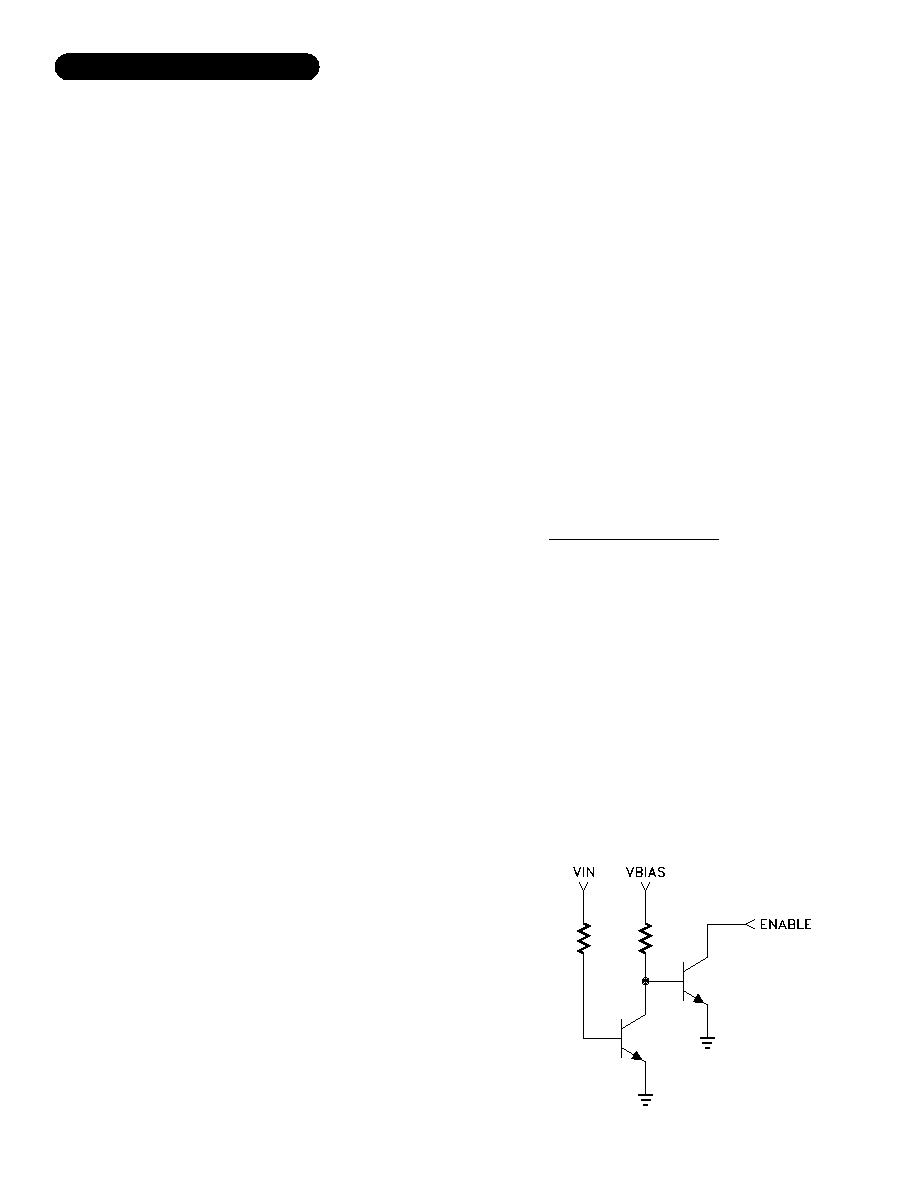
The soft start will begin as soon as the bias voltage
exceeds the under voltage lockout threshold or the in-
hibit pin is released; whichever comes last. If bias volt-
age is applied and the inhibit pin is released before the
input voltage is applied, the soft start will have risen
early and the output will rise at approximately the same
rate as VIN and may overshoot. Any circuit that holds
the enable pin low until VIN rises will ensure soft start
when VBIAS must rise before VIN. The circuit below
may be adapted to suit a variety of applications.
APPLICATION NOTES CONT'D
PRELIMINARY Rev. G 2/06
4
SENSE:
ENABLE FUNCTION:
The ENABLE pin of the MSK 5046RH is designed for
open collector drive. Leaving the pin open will allow for
normal operation. Pulling the pin low will shut the de-
vice down. The enable pin will source up to 3mA when
pulled low with high line voltage.
It is very important that the DC voltage returned to
the SENSE pin from the output be as noise and oscilla-
tion free as possible. This voltage helps to determine
the final output and therefore must be a clean voltage.
Excessive noise or oscillation can cause the device to
have an incorrect output voltage. Proper PC board lay-
out techniques can help to achieve a noise free voltage
at the SENSE pin.
CURRENT LIMIT:
The MSK 5046RH current limit is user programmable
by means of an external low value sense resistor. The
current limit trips at approximately 100mV, ±20% across
the sense resistor. The output voltage will decrease when
the current limit is reached. In the case of a sudden and
severe overload, the MSK 5046RH will reset and attempt
a restart cycle. In noisy systems, the use of a twisted
pair helps reduce noise succeptability of the sense cir-
cuit. The voltage present on the sense resistor will have
an AC component at the switching frequency. The peak
of the AC plus DC voltage will trip the current fault. If
current limit is not desired, simply connect CS+ to ground
and CS- to VOUT to disable the current sense.
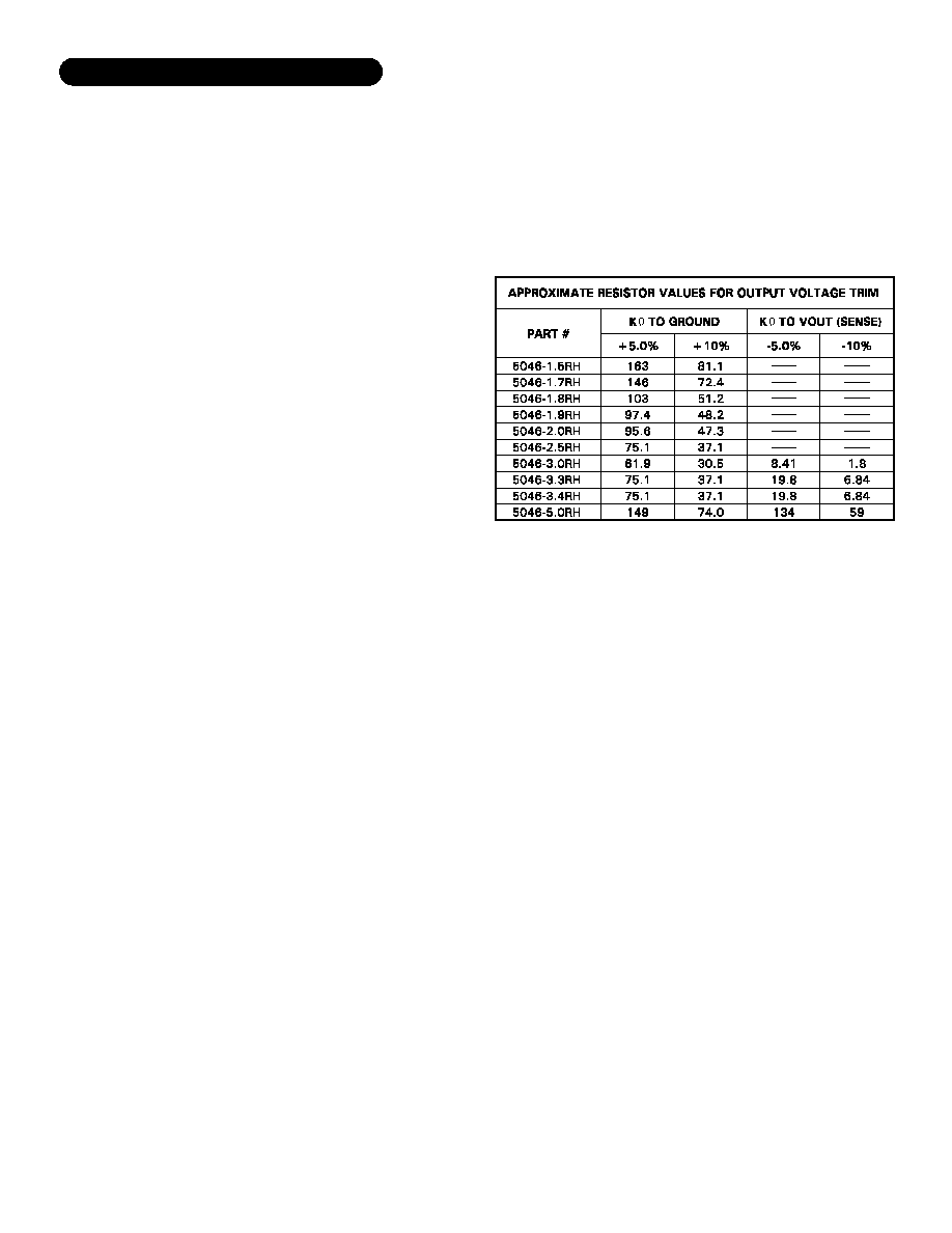
ADJUST:
The output voltage of the MSK5046RH may be ad-
justed up or down to accomodate a variety of system
requirements. Connecting a resistor between the adjust
pin and the sense pin will decrease the output voltage.
Connecting a resistor between the adjust pin and ground
will increase the output voltage.
MINIMUM LOAD:
The MSK 5046RH requires less than 2mA minimum
load to maintain regulation. Minimum loads greater than
200mA at low line voltage and 400mA at high line volt-
age provide faster load response.
APPLICATION NOTES CONT'D
TYPICAL LOW VOLTAGE APPLICATION
PRELIMINARY Rev. G 2/06
5
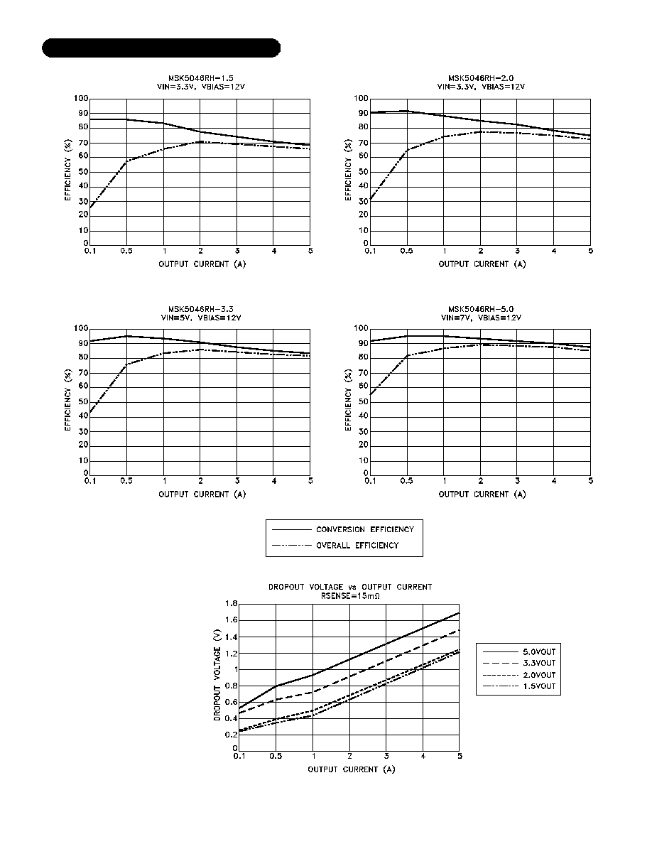
TYPICAL PERFORMANCE CURVES
PRELIMINARY Rev. G 2/06
6
NOTE: Overall efficiency curves include VBias power consumption.

RADIATION CURVES
PRELIMINARY Rev. G 2/06
7
TBD
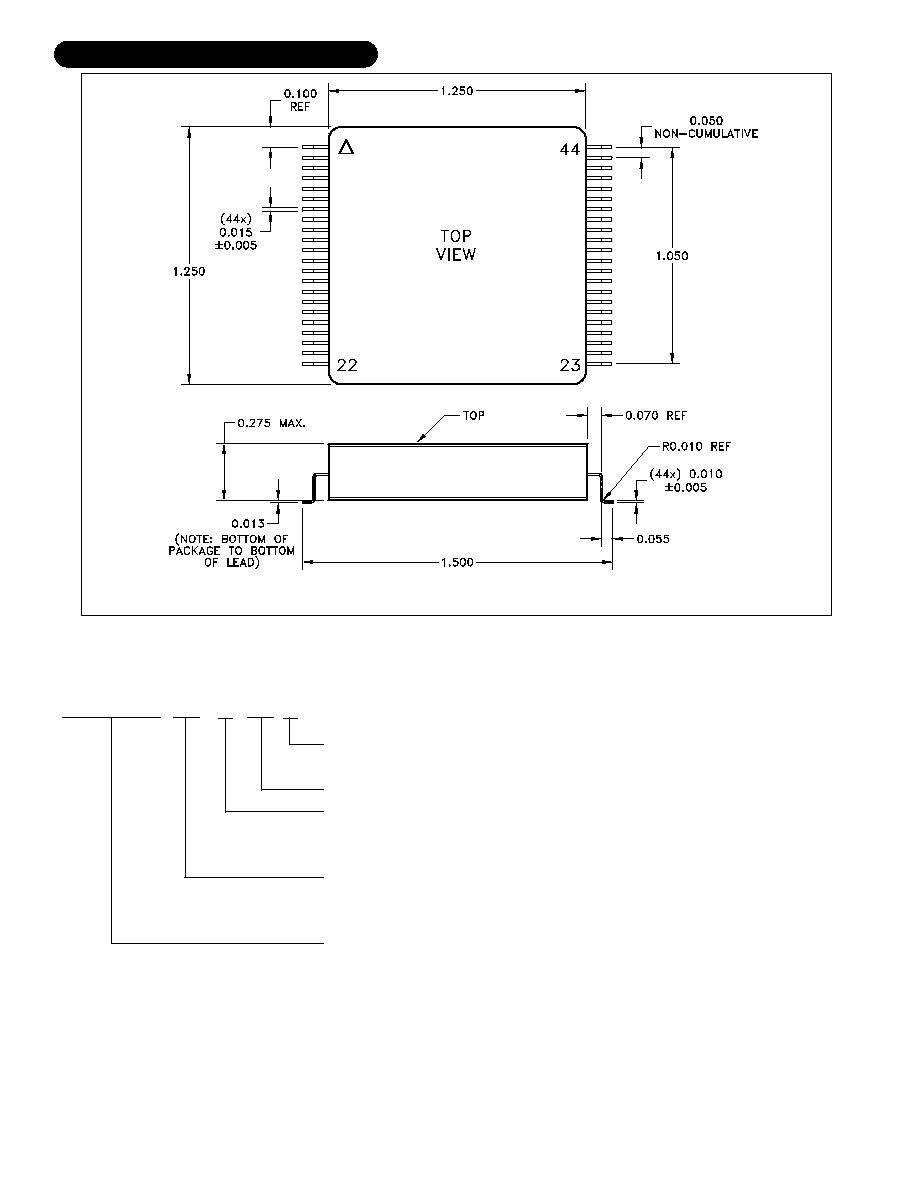
MECHANICAL SPECIFICATIONS
PRELIMINARY Rev. G 2/06
The above example is a +3.3V, Class H screened regulator with gull wing leads.
ESD Triangle indicates Pin 1.
NOTE: ALL DIMENSIONS ARE ±0.010 INCHES UNLESS OTHERWISE LABELED.
ORDERING INFORMATION
8
MSK5046-3.3 H RH G
LEAD FORM OPTIONS
BLANK=STRAIGHT; G=GULL WING
RADIATION HARDENED
SCREENING
BLANK= INDUSTRIAL; E=EXTENDED RELIABILITY
H=MIL-PRF-38534 CLASS H; K= MIL-PRF-38534 CLASS K
OUTPUT VOLTAGE
1.5=+1.5V; 1.7=+1.7V; 1.8=+1.8V; 1.9=+1.9V; 2.0=+2.0V;
2.5=+2.5V; 3.0=+3.0V; 3.3=+3.3V; 3.4=+3.4V; 5.0=+5.0V
GENERAL PART NUMBER
WEIGHT= 17 GRAMS TYPICAL
The information contained herein is believed to be accurate at the time of printing. MSK reserves the right to make
changes to its products or specifications without notice, however, and assumes no liability for the use of its products.
Please visit our website for the most recent revision of this datasheet.
Contact MSK for MIL-PRF-38534 Qualification and Appendix G (radiation) status.
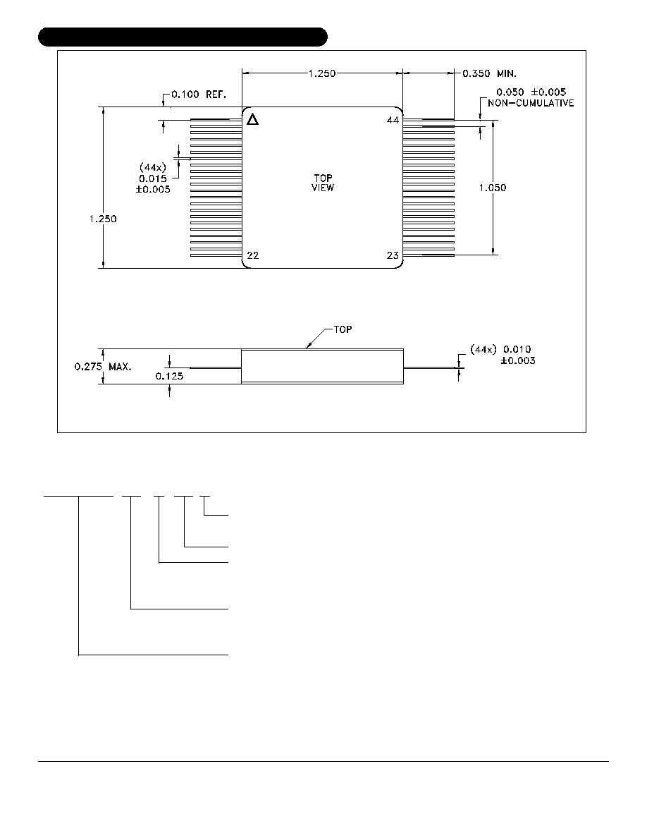
MECHANICAL SPECIFICATIONS CONTINUED
M.S. Kennedy Corp.
4707 Dey Road, Liverpool, New York 13088
Phone (315) 701-6751
FAX (315) 701-6752
www.mskennedy.com
PRELIMINARY Rev. G 2/06
The above example is a +3.3V, Class H screened regulator.
ESD Triangle indicates Pin 1.
NOTE: ALL DIMENSIONS ARE ±0.010 INCHES UNLESS OTHERWISE LABELED.
ORDERING INFORMATION
9
MSK5046-3.3 H RH
LEAD FORM OPTIONS
BLANK=STRAIGHT; G=GULL WING
RADIATION HARDENED
SCREENING
BLANK= INDUSTRIAL; E=EXTENDED RELIABILITY
H=MIL-PRF-38534 CLASS H; K= MIL-PRF-38534 CLASS K
OUTPUT VOLTAGE
1.5=+1.5V; 1.7=+1.7V; 1.8=+1.8V; 1.9=+1.9V; 2.0=+2.0V;
2.5=+2.5V; 3.0=+3.0V; 3.3=+3.3V; 3.4=+3.4V; 5.0=+5.0V
GENERAL PART NUMBER
WEIGHT= 17 GRAMS TYPICAL