4707 Dey Road Liverpool, N.Y. 13088
M.S.KENNEDY CORP.
(315) 701-6751
FEATURES:
5102
SERIES
HIGH CURRENT,
LOW DROPOUT
VOLTAGE REGULATORS
Extremely Compact 10 Pin Flatpack With Metal Base
Extremely Low Dropout Voltage: 350mV @ 1.5 Amps
Available in +1.5V, +1.7V, +1.9V, +2.5V, +3.3V, +5.0V and +12.0V
TTL Level Enable Pin: Zero Current Shutdown Mode
Reverse Battery and Load Dump Protection
Low Ground Current: 32mA Typical at Full Load
1% Guaranteed Accuracy
Output Current to 1.5 Amps
MIL-PRF-38534 CERTIFIED
DESCRIPTION:
The MSK 5102 series voltage regulators are available in +1.5V, +1.7V, +1.9V, +2.5V, +3.3V, +5.0V and +12.0V
configurations. All boast ultra low dropout specifications due to the utilization of a super PNP output pass transistor with
monolithic technology. Dropout voltages of 350mV at 1.5 amps are typical in this configuration, which drives efficiency up
and power dissipation down. Accuracy is guaranteed with a 1% output voltage tolerance. The series also offers a TTL/
CMOS compatible on/off enable function. The MSK 5102 series is packaged in a space efficient 10 pin ceramic flatpack
with a built in metal base.
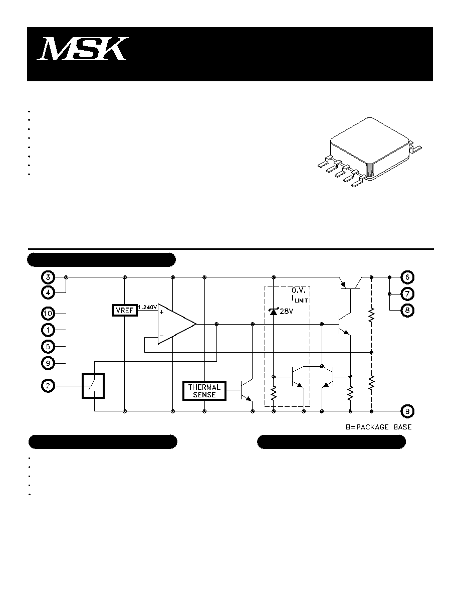
EQUIVALENT SCHEMATIC
TYPICAL APPLICATIONS
PIN-OUT INFORMATION
High Efficiency, High Current Linear Regulators
Constant Voltage/Current Regulators
System Power Supplies
Switching Power Supply Post Regulators
Battery Powered Equipment
NC
Enable
Vin A
Vin B
NC
Vout A
Vout B
Vout C
NC
NC
1
2
3
4
5
6
7
8
9
10
BASE
The base of the package is electrically
connected to ground.
Rev. B 2/06
1
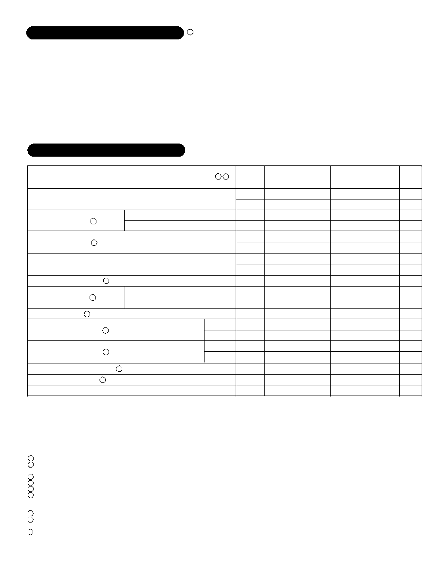
Output Voltage Tolerance
Dropout Voltage
Load Regulation
Line Regulation
Ground Current
Enable Input Voltage
Enable Input Current
Output Current Limit
Output Noise
Shutdown Output Current
Thermal Resistance
Thermal Shutdown
Input Voltage (100mS 1%D.C.)
Input Voltage
Enable Voltage
Output Current
Storage Temperature Range
Lead Temperature
(10 Seconds Soldering)
Operating Temperature
MSK5102 Series
MSK5102H/E Series
Group A
Subgroup
1
2,3
1
1
1
2,3
1
2,3
-
-
-
-
1
1
1
1
-
-
-
%
%
mV
mV
%
%
%
%
A
mA
mA
µV
V
V
µA
µA
µA
∞C/W
∞C
V
OUT
=-1%; I
OUT
=
100m
A
V
OUT
=-1%; I
OUT
=1.5A
V
IN
=V
OUT
+1V
10mA
I
OUT
1.25A
(V
OUT
+1V)
V
IN
26V
I
OUT
=10mA
V
OUT
=0V; V
IN
=V
OUT
+1V
V
IN
=V
OUT
+1V; I
OUT
=0.75A
V
IN
=V
OUT
+1V; I
OUT
=1.5A
C
L
=10µF; 10Hz
f
100KHz
V
ENABLE
0.8V
Junction to Case @ 125∞C
T
J
-20V to +60V
26V
-0.3V to 26V
3.5A
V
INP
V
IN
V
EN
I
OUT
Parameter
T
ST
T
LD
T
J
ELECTRICAL SPECIFICATIONS
ABSOLUTE MAXIMUM RATINGS
-65∞C to +150∞C
300∞C
-40∞C to +85∞C
-55∞C to +125∞C
1
Test Conditions
1
2
3
4
5
6
7
8
9
NOTES:
Output decoupled to ground using 10µF minimum capacitor unless otherwise specified.
This parameter is guaranteed by design but need not be tested.
Typical parameters are representative of actual device performance but are for reference only.
All output parameters are tested using a low duty cycle pulse to maintain T
J
= T
C
.
Industrial grade and class E devices shall be tested to subgroups 1 and 4 unless otherwise specified.
Military grade devices ('H' suffix) shall be 100% tested to subgroups 1,2,3 and 4.
Subgroup 1,4
Subgroup 2
Subgroup 3
Please consult factory if alternate output voltages are desired.
Due to current limit, maximum output current may not be available at all values of V
IN
-V
OUT
and temperatures. See typical
performance curves for clarification.
Continuous operation at or above absolute maximum ratings may adversely effect the device performance and/or life cycle.
T
C
=+25∞C
T
J
=+125∞C
T
A
=-55∞C
HIGH/ON
LOW/OFF
HIGH/ON
LOW/OFF
MSK 5102H/E SERIES
Min.
-
-
-
-
-
-
-
-
-
-
-
-
2.4
-
-
-
-
-
-
Typ.
±0.5
±1.0
80
350
±0.2
±0.3
±0.05
±0.5
2.1
18
32
400
-
-
100
-
10
5.6
135
Max.
±1.0
±2.0
200
600
±1.0
±2.0
±0.5
±1.0
3.5
30
-
-
-
0.8
600
2
500
6
-
Typ.
±0.5
-
80
350
±0.2
±0.3
±0.05
±0.5
2.1
18
32
400
-
-
100
-
10
5.6
135
MSK 5102 SERIES
Min.
-
-
-
-
-
-
-
-
-
-
-
-
2.4
-
-
-
-
-
-
Max.
±1.0
-
225
625
±1.2
-
±0.6
-
3.5
30
-
-
-
0.8
600
2
500
7
-
Units
2
2
2
2
3
I
OUT
=10mA; V
IN
=V
OUT
+1V
2
Rev. B 2/06
2
2
2
2
8
9

APPLICATION NOTES
HEAT SINK SELECTION:
To select a heat sink for the MSK 5102, the following formula
for convective heat flow may be used.
Governing Equation:
Tj = Pd x (R
jc + R
cs + R
sa) + Ta
WHERE:
Tj = Junction Temperature
Pd = Total Power Dissipation
R
jc = Junction to Case Thermal Resistance
R
cs = Case to Heat Sink Thermal Resistance
R
sa = Heat Sink to Ambient Thermal Resistance
Ta = Ambient Temperature
REGULATOR PROTECTION:
The MSK 5102 series is fully protected against reversed input
polarity, overcurrent faults, overtemperature conditions (Pd) and
transient voltage spikes of up to 60V. If the regulator is used in
dual supply systems where the load is returned to a negative
supply, the output voltage must be diode clamped to ground.
OUTPUT CAPACITOR:
The output voltage ripple of the MSK 5102 series voltage regu-
lators can be minimized by placing a filter capacitor from the
output to ground. The optimum value for this capacitor may
vary from one application to the next, but a minimum of 10µF is
recommended for optimum performance. Transient load response
can also be improved by placing a capacitor directly across the
load.
LOAD CONNECTIONS:
In voltage regulator applications where very large load currents
are present, the load connection is very important. The path
connecting the output of the regulator to the load must be
extremely low impedance to avoid affecting the load regulation
specifications. Any impedance in this path will form a voltage
divider with the load.
ENABLE PIN:
The MSK 5102 series of voltage regulators are equipped with a
TTL compatible ENABLE pin. A TTL high level on this pin acti-
vates the internal bias circuit and powers up the device. A TTL
low level on this pin places the controller in shutdown mode
and the device draws approximately 10µA of quiescent current.
If the enable function is not used, simply connect the enable pin
to the input.
First, the power dissipation must be calculated as follows:
Power Dissipation = (Vin - Vout) x Iout
Next, the user must select a maximum junction temperature.
The maximum allowable junction temperature is 125∞C. The
equation may now be rearranged to solve for the required heat
sink to ambient thermal resistance (R
sa).
EXAMPLE:
An MSK 5102-3.3 is configured for Vin=+5V and
Vout=+3.3V. Iout is a continuous 1A DC level. The ambient
temperature is +25∞C. The maximum desired junction tem-
perature is 125∞C.
R
jc = 6∞C/W and R
cs = 0.5∞C/W typically.
Power Dissipation = (5V - 3.3V) x (1A)
Solve for R
sa:
R
sa = 125∞C - 25∞C - 6∞C/W - 0.5∞C/W
In this example, a heat sink with a thermal resistance of no more
than 52∞C/W must be used to maintain a junction temperature
of no more than 125∞C.
1.7W
= 1.7 Watts
DEVICE SOLDERING/CASE CONNECTION:
The MSK 5102 series are highly thermally conductive devices
and the thermal path from the package base to the internal junc-
tions is very short. Standard surface mount techniques should
be used when soldering the device into a circuit board. The
external heat sink/pad needs to be connected to ground because
the base of the MSK 5102 is also electrically connected to
ground. The user is urged to keep this in mind when designing
the printed circuit board for the MSK 5102. There should be no
printed circuit traces making contact with the base of the device
except for ground. The ground plane can be used to pull heat
away from the device.
Rev. B 2/06
3
= 52.3∞C/W
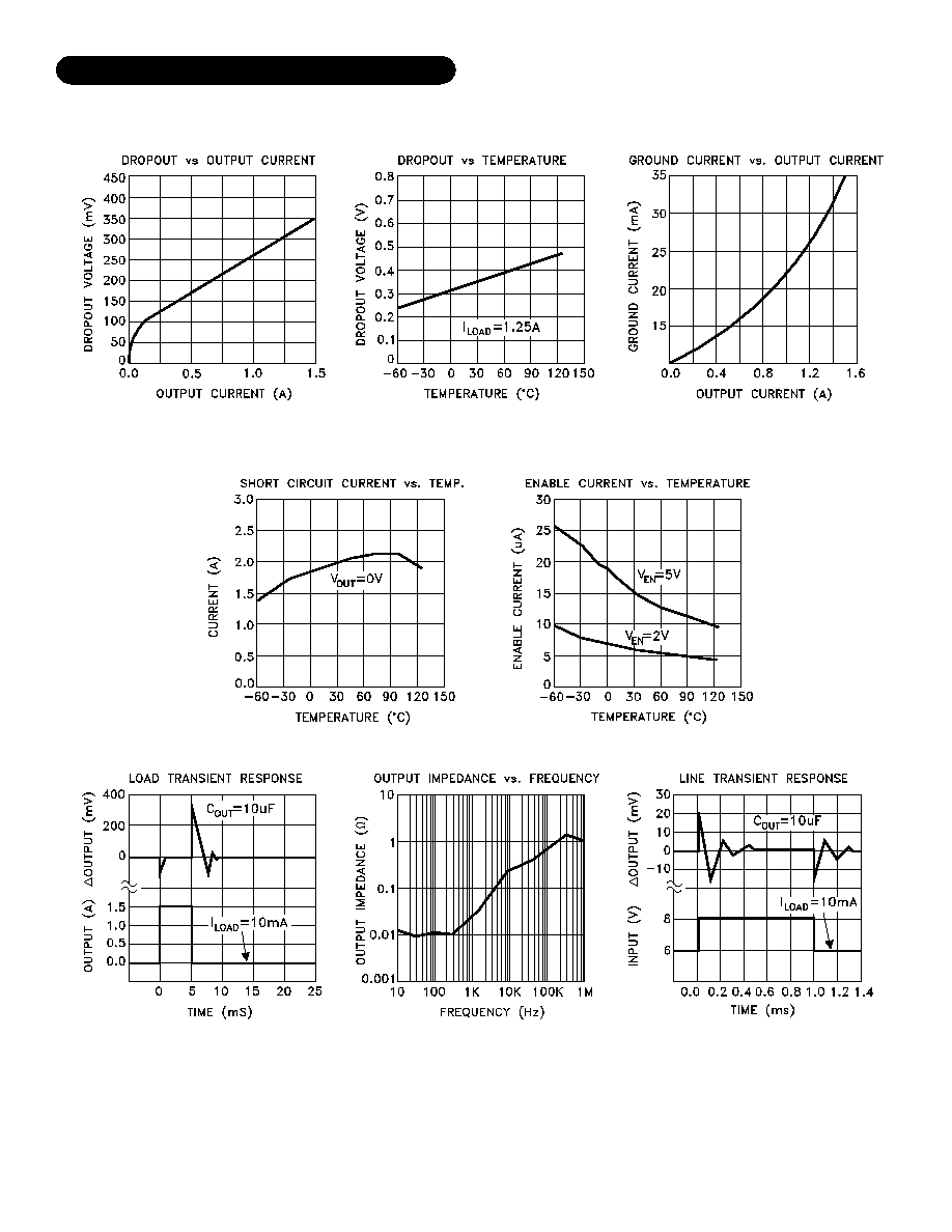
TYPICAL PERFORMANCE CURVES
Rev. B 2/06
4
The information contained herein is believed to be accurate at the time of printing. MSK reserves the right to make
changes to its products or specifications without notice, however, and assumes no liability for the use of its products.
Please visit our website for the most recent revision of this datasheet.
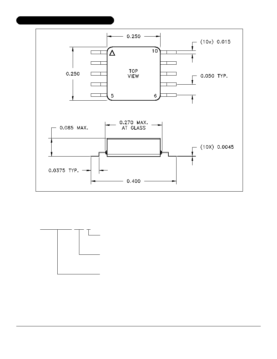
MECHANICAL SPECIFICATIONS
M.S. Kennedy Corp.
4707 Dey Road, Liverpool, New York 13088
Phone (315) 701-6751
FAX (315) 701-6752
www.mskennedy.com
NOTE: ALL DIMENSIONS ARE ±0.010 INCHES UNLESS OTHERWISE LABELED.
ESD Triangle indicates Pin 1.
MSK5102-3.3 H
The above example is a +3.3V, Military regulator.
ORDERING INFORMATION
SCREENING
BLANK=INDUSTRIAL, E=EXTENDED RELIABILITY;
H=MIL-PRF-38534 CLASS H
OUTPUT VOLTAGE
1.5=+1.5V; 1.7=+1.7V; 1.9=+1.9V; 2.5=+2.5V
3.3=+3.3V; 5.0=+5.0V; 12=+12.0V
GENERAL PART NUMBER
Rev. B 2/06
5
WEIGHT= 0.3 GRAMS TYPICAL